Note : Les descriptions sont présentées dans la langue officielle dans laquelle elles ont été soumises.
~X~
ETCHING PROCESS FOR FABRICATING INTEGRATED-CIRCUIT
DEVICES UTILIZING MULTILEVEL RESIST STRUCTURE
AND EMPLOYING CARBON DIOXIDE PLASMA
Backqround of the Invention
This invention relates to a proces for making integrated-
circuit devices utilizing multilevel resist structure.
Increasing miniaturization of semiconductor integrated-
circuit devices is the basis for reduced unit cost per
function and for improved performance. Feature sizes in very-
large-scale-integrated (VLSI) devices thus continue to get
smaller. Some predict that minimum feature sizes in VLSI
devices in actual production will certainly be less than one
micrometer (~m~ before 1990.
As feature sizes of VLSI devices decrease, processing
requirements for fabricating the devices become more critical.
These requirements include the availability of resists
characterized by extremely high sensitivity and resolution.
Moreover, for improved resolution and linewidth control, such
resists must in many cases of practical importance be included
in multilevel resist structures such as the so-called trilevel
structure described in U.S. Patent No. 4,244,799 and in "High
Resolution, Steep Profile, Resist Patterns" by J. M. Moran and
D. Maydan, The Bell System Technical Journal Vol. 58, No. 5,
May-June 1979, pages 1027-1036. Such a trilevel structure
typically includes a top resist layer, an intermediate masking
layer and a bottom planarizing 1ayer.
In a trilevel structure as heretofore proposed, a
lithographically de~ined pattern in the resist layer is ~irst
transferred into the intermediate masXing layer. Subsequent-
ly, utilizing the pattern in the intermediate layer as a mask,
the planarizing layer is patterned. This last-mentioned
transfer step is, for example, carried out in a reaction
chamber by dry etching techniques utilizing an oxygen plasma
~ to pattern the planarizing layer, as described in the
; 35 aforedescribed references.
, ~
~,.
, :
.
; ' , ~ ` '
`' "` ' ',. `
.
.
~28~6~2
As feature sizes in integrated-circuit devlces decrease
to one ~m and below, it has become exceedingly difficult
in practice to maintain high-quality linewidth control at
relatively high etching rates when utilizing an oxygen
plasma to pattern the planarizing layer of a multilevel
resist structure. By adjusting the rate of flow of oxygen
into the reaction chamber and the value of the bias voltage
on the electrode that holds the device to be etched, the
~2~g~82
characteristics of the etching process can be selectively
varied. But adequate linewidth control is usually achieved in
this manner at the expense of etchlng rate. And attempts to
increase etching rate typically degrade linewidth control and
also may cause radiation damage to the device being etched.
Accordingly, efforts have been directed by workers
skilled in the art at trying to devise improved etching
techniques for transferring a pattern into the planarizlng
layer of a multilevel resist structure. In particular, these
lo efforts have been directed at trying to achieve good linewidth
control, high etching rates and negligible radiation damage to
the device being etched. It was recognizecl that these
efforts, if successful, had the potential to significantly
increase the quality and decrease the cost of extremely fine-
featured integrated-circuit devices.
; Summary of the_Invention
The present in~ention ~mbodi~s an improved process for
making integrated-circuit devices and includes transferring a
fine-featured pattern defined in resist into the planarizing
layer of a multileYel resist structure.
In accordanca with one aspect of the invention there is
provided a method for fabricating an integrated-circuit device
comprising the steps of forming a multilevel structure that
includes a relatively thin patterned masking layer comprising
a material selected from the group consisting of resist
material and silicon dioxide overlying a relatively thick
planarizing layer comprising a hardened polymer on a
substrate, forming a pattern including at least one structure
having a dimension of 1 micron or less in said thin patterned
masking layer, transferrinq said pattern by anisotropically
etching said planarizing layer in a reaction chamber in a
plasma derived from carbon dioxide to trans~er the pattern of
said relatively thin masking layer into said relatively thick
planarizing layer, wherein the resolution of said pattern
during said transfer is not substantially degraded, and
.
- - , . - .
, ' ' ', '
~ .
. ' , , '' ' ' ' ..
,
12896~32
wherein the time taken to effect said transfer is not
substantially longer compared to the time required to transfer
said pattern with the same resolution utilizing an oxygen
plasma.
The present invention is described with reference to a
specific illustrative embodiment thereof in which the
planarizing layer of a multilevel-resist structure formed on
an integrated-circuit device is anisotropically patterned in a
reactive-ion-etching step in a reaction chamber in a plasma
derived from carbon dioxide. Pure carbon dioxide gas
introduced into the chamber is e~fective to etch the layer at
a relatively high rate with good linewidth control and
negligible radiation damage to the device. But, in accordance
with the principles of the present invention, anisotropic
etching of the planarizing layer can also be effectively
carried out in a plasma derived from at least approximately
ten percent by volume carbon dioxide combined with an inert
gas. Except for a slightly lower etching rate, such a
; combination of gas provides the same advantages as those
specified above for pure carbon dioxide.
A complete understanding of the present invention and of
the above and other features and advantages thereof may be
gained from a consideration of the following detailed
description presented hereinbelow in connection with the
accompanying single~figure drawing, which is not drawn to
scale.
` ,.i~'~'
.;.
~: . .
~ ' ` ' .
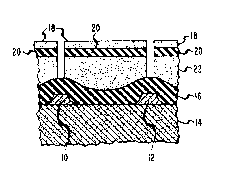
The drawing schematically represents a portion of a standard integrated-
circuit device that comprises conductive elements 10 and 12 disposed on a
substrate 14. Deposited on the top surface of the substrate 14 and covering the
elements 10 and 12 is a layer 16 made of a conventional dielectric material such5 as p-doped glass~
In accordance with standard steps of a known device fabrication
sequence, openings or windows are to be formed in the layer 16 in aligned
registry with the underlying conductive elements 10 and 12. A conductive
material such as aluminum will then be deposited Oll the top surface of the
10 de~ice and in the aligned windows to establish electrical connections from an upper level of the device structure to the elements 10 and 12.
A trilevel resist structure of the type described in the aforecitecl U.S.
Patent 4,2'14,7~ and in Moran et al article i9 a particularly advantageous way of
patterning the layer 16. As indicated in the drawing, such a known trilevel
15 structure includes, from top to bottom, layers 18, 20, and 22.
The layer 18 shown in the drawing comprises a positive or ne~atlve resist
material that can be selecti~ely patterned by, for example, directing light,
electrons, X-rays, or ions thereat. A wide variety of such materials is well
known in the art. Many standard techniques are available for selectively
20 exposing and developing these materials to form a specified high-resolution
pattern in the layer 18.
The intermediate layer 20 in the known structure shown in the drawing
comprises, for example, a 120 nm-thick layer of plasma-deposited silicon dioxide.
In standard ways, the pattern in the resist layer 18 is transferred into the
25 layer 20 by dry etching techniques. Illustratively, this is done by either plasma
or reactive-ion etching the layer 20 with, for example, C~3, utilizing the
patterned layer 18 a~ a dry-etch-resistant mask therefor.
The planarizing layer 22 included in th~ ~tandard depicted structure
comprises, for example, a relatively thick layer of an organic material. A
30 number of available organic materials such as a variety oî polymers are suitable
for forming the layer 22. Such materials include a variety of known re~ists and
polyimides. Illustratively, the layer 22 comprises a 1.8-,um-thick layer of HPR-206 which, after deposition, is, îor example, baked for about 20 minutes at
approximately 210 degrees aelsiu~. HPR-20~ is r. strndsrd positivs photorssist
:, .. .
. : . . . .
~89613~
- 4 --
commercially available from Philip A. Hunt Chemical Corporation, Palisades
Park, New Jersey.
The pattern in the layer 20 is transferred into the thick layer 22 in a dry
etching step. Conventionally, this is done, for example, in a reactive-ion-etching
5 step utilizing pure oxygen to form a plasma, with the patterned layer 20 acting
as a mask.
A conventional trilevel structure of the type shown in the drawing and
described above is an important factor in being able in practice to achieve
submicron lithography. Unfortunately, however, as specified earlier above, it
10 has become exceedingly difrlcult in practice to maintain high-quality linewidth
control at relatively high etching rates when utilizing an oxygen plasma to
pattern features of one ,um and below in the planarizing layer 22.
In accordance with the principles of the present invention, a carbon
dioxide plasma rather than an oxygen plasma is ut;lized to pattern the
15 planari~ing layer 22 of the multileYel resist structure showII in the drawing.
Illustratively, patterning of the layer 22 is carried out in a reactive-ion-etching
step utilizing at least approximately ten percen$ carbon dioxide gas by volume
When less than pure carbon dioxide is utilized, it is mixed with an inert gas
such a~ helium or argon.
By way of example, the device to be etched in accordance with
applicant's invention is placed in the reaction chamber of a standard reactive-
ion-etching system. Illustratively, the device is placed on the cathode electrode
of a so-called hex reactor of the type manufactured by Applied Materials, Inc.,
Santa Clara, California This reactor is designated by Applied Materials as its
25 AME 8100 Series Plasma Etch System
In accordance with the principles of applicant's invention, the direct-
current bias on the aforementioned cathode electrode in the reaction chamber is
established at a value in the range of about 45~to-550 volts The flow of
carbon dioxide into the chamber is controlled to be approximately 10~to-150
30 standard cubic centimeters per m;nute. And the pressure w;thin the chamber is maintained at about 1.33 to 2.67 Pa ~1~to-20 milliTorr)
For the illustrative condition~ specified above, the planarizing layer 22 of
the device shown in the drawing is etched at a rate of about 5~to-6S nm per
minute. This etching rate has been observed to be load dependent; that is, the
.
.
. . , . . . . . . -. .
8~
-- 5 --
etch rate increases as the exposed surface area of the layer 22 to be etched
decreases.
Etching carried out in accordance with applicant's invention as specirled
above produces essentially vertical walls in the planarizing layer 22 with
5 substantially no undercutting thereof. Linewidth loss during etching with
carbon dioxide has been determined to be extremely small, ranging in practice
from O~to-0.05 ,um. ~oreover, applicant's etching process as described herein
has been observed to e~hibit excellent uniformity and reproducibility and to
have a very low sensitivity to process parameter variations. Further, devices
10 etched by this process have been determined to suîfer negligible radiation
damage .
In some cases involving patterning of a multilevel resist structure,
polymér build-up may occur on the walls or on other surfaces of the reaction
chamber. Such build-up stems, for example, from standard CHF3 etching of the
15 intermediate masking layer 20. In those cases, it ~nay be advalltageous, prior to
commencing etching of the exposed layer 22 with carbon dioxide in the
particular manner specil~led above, to establish an oxygen plasma in the
chamber for several minutes to remove any polymer that has formed within the
chamber. A conventional oxygen plasma etching step of the type priorly
20 employed in the art to etch through the entire thickness of the layer 22 is
effective to remove such build-up. Surface portions of the layer 22 will also
thereby be etched. But, in accordance with the principles of the present
invention, the major extent of the thickness of the layer 22 is then etched withcarbon dioxide in the particular manner described above.
Fînally, it is to be understood that the above-described str~ctures and
processing techniques are only illustrative of the principles of the present
invention. In accordance with these principles, numerc>us modifications and
alternatives may be devised by those skilled in the art without departing from
the spirit and scope of the invention~ For example, although primary emphasis
30 herein has been d}rected to a multilevel resist structure of the trilevel type, it is
to be understood that applicant's inventive principles are also applicable to so-
called bilevel resist structures. In a bilevel structure, a patterned resist layer
such as the layer 18 shown in the drawing directly overlies a planarizing layer
such as the layer 22 described herein. Additionally, for proflle control purposes,
~8~6~3~
- 6 ^
it may be advantageous in some cases of practical importance to add some
oxygen to carbon dioxide to form a plasma for etching the planarizing layer. :
:
.
,
:.
.
,.,