Note : Les descriptions sont présentées dans la langue officielle dans laquelle elles ont été soumises.
d~
FAST ENTRY TO EMULATION
Robert Maier
John Andoh
Arno Krakauer
Richard Tobias
Allan Zmyslowski
.
Field of the Invention
The present invention relates to data processing
machines that run with system control programs implementing
logical processors. Each logical processor is assigned a
domain including storage space and related facilities in
the data processing machine. The present invention in
particular relates to the accessing of domain storage
space.
Back round of the Invention
g
Modern high speed data processing machines are being
adapted for multi-user environments. One approach for
adapting a single machine to a multi-user environment
involves assigning a logical processor to each user. The
logical processor behaves as if it had access to the full
facilities of the data processing machine while system
control confines the access of the logical processor to a
specified domain of storage space and related hardware. In
this manner, the various logical processors in a single
machine do not overlap in storage. However, to simplify
the user interface, the restricted access o the logical
processor is transparent to that processor. Thus,
instructions and addresses running in the machine do not
specify a particular domain within which they are to be
executed or used for accessing data.
AMDH-5464DEL/MAH
03/SJW2 100886
,. ~ . .. .
?~,3~
P domain is a processing environment which consists of
main storage, channels, operator facilities and logical
processors that execute instructions. When activated in a
preferred embodiment, a domain has the facilities described
in the IBM System/370 Principles of Operation, or the IBM
System/370 ~xtended Architecture Principles of Operation.
These resources are controlled by a system control program
and are collectively called the domain of the program.
When a system control program takes over in a machine,
its domain is activated by macrocode, allocating the amount
of storage, the number of channels and logical processors
required. The system control programs and macrocode
allocating a domain operate in a machine state called
control state. Control state has dedicated main storage
ealled system s~orage which is addressPd with system
addresses.
Programs run in a logical processor, known as domain
programs, operate in a machine state called user state.
The main storage allocated to a domain is called domain
storage and domain storage accesses use domain addresses.
At times it is necessary for a program running in
control state to access data stored in domain storage.
This occurc~ for instance, during emulation as discussed
below.
A data processing machine is designed to implement a
set of instructions known as machine instructions. After
the architecture of the machine is defined, it is often
desirable to implement instructions other than those in the
machine set. This is accomplished by storing an emulation
program of instructions in system storage that can be run
in control state to emulate a new instruction.
* Trade Mark
~, ,.~ -
AMDH-5464DEL/MAH
03/SJW2 100886
--3--
W~en an instruction to be emulated is encountered by a
logical processor, a bran~h to the control state is taken
and the instruction is emulated.
Upon branch to the control state, it is necessary to
test for program exceptions that apply to the emulation
routine to be run in the control state. These tests take
several lines of code in the emulation program and result
in a decrease in performance of emulated instructions.
Also, in order to emulate some instructions, it is
necessary for the emulation program in system storage
running in the control state to access operands or other
data stored in domain storage.
As discussed above, the instructions and addresses
generated by logical processors do not specify whether a
particular address is to be treated as a domain address or
a system address.
In order to provide for this domain crossing during
emulation, the prior art specified special instructions for
emulation that operated in the control state and provided
for access to domain storage. However, this implementation
of special instructions resulted in only a limited number
of instructions that could implement the domain crossing
access and was costly to implement.
S_mmary of the Invention
The present invention provides a new technique called
implied domain addressing to differentiate between domain
storage accesses and system storage accesses using existing
instruction formats.
In one aspect, the present invention is a data
processing apparatus, having a user domain with domain
storage space and an emulation domain with emulation
storage space, ~or processing a sequence of instructions.
AMDH-5464DEL/MAH
03/SJW2 100886
The sequence of instructions includes an instruction in the
user domain that calls an emulation program of instructions
in the emulation domain. The apparatus comprises an
instruction register connected to receive the sequence of
instructions, including a plurality of fields. At least
one field of the instruction register identifies a location
for address information for an operand used in execution of
the instruction. Decoding means, connected to receive the
instruction to be emulated, decodes the instruction to
generate a control code. The control code includes a
branch signal to call the program of instruction in the
emulation domain and a domain access control signal to
indicate whether the program of instructions in the
emulation domain requires access to the user domain storage
space for execution.
In response to the branch signal, the program of
instructions from the emulation domain is supplied in
sequence to the instruction register. In response to the
domain access control signal and the location identified in
the one field in the instruction register, a user domain
access signal is generated indicating whether, for each
instruction in the sequence, access to the user domain is
required.
Addressing means in the data processing apparatus in
communication with the instruction registerl supplies an
address for an operand stored in a storage means. The
storage means, connected to receive the user domain access
control signal and the operand address, stores operands
from the user domain and the emulation domain at locations
identified by the addresses. The addresses are translated
in storage means in control state normally as emulation
domain addresses. However, a means according to the
present invention is included that is responsive to the
AMDH-5464DEL/MAH
03/SJW2 100886
user domain access signal for translating the address as a
user domain address.
In another aspect, the present invention is a data
processing apparatu~s as outlined above in which testing for
program e~ceptions upon entry to an emulation program is
accomplished quickly upon branch to the control state. The
decoding means is responsive to the instruction to be
emulated to generate a control code that includes a branch
signal and a branch test signal. In means response -to the
branch signal for branching program control of the
apparatus to the second ox emulation state to enter a fast
program for emulating the instruction. A means receiving
the branch test signal tests for program exceptions upon
branch to the emulation state apart from the fast program
entered upon branch to emulation state. Upon detection of
a program exception, an additional branch to an alternate
program of instructions to handle the program exceptions
and special cases is taken. In this manner, entry into an
emulation program occurs quickly and emulation proceeds
efficiently. Only upon detection of a program exception is
a more cumbersome entry to the emulation program required.
With implied domain addresslng, the instruction set
capable of use in accessing domain storage during emulation
of an instruction in a control state is extended to include
essentially all instructions which are capable of accessing
system storage. With the addition of fast testing for
program exceptions, emulation performance is greatly
enhanced.
Brief Description of the Figures
Fig. 1 is an overview block diagram of a data
processing machine implementing the present invention.
AMDH-5464DEL/MAH
03/SJW2 100886
--6--
Fig. 2 is a schematic block diagram showing data flow
during entry to an emulation program.
Fig. 3 is a schematic block diagram illustrating data
flow during storage access.
5Fig. 4 is a more detailed diagram of logic
implementing implied domain storage access.
Fig. 5 is a logic diagram of the instruction unit -
storage unit interface during domain storage access.
Fig. 6 is a schematic diagram illustrating tests
performed during entry to an emulation program.
Fig. 7 is a logic diagram illustrating implementation
of the tests performed during entry to an emulation
program.
15Detailed Description
With reference to the figures, a detailed description
of a preferred embodiment is provided. First, with
reference to Fig. 1, the data processing system environment
of the present invention is described. With reference to
Fig. ~, a part of the apparatus of the present invention is
described that operates during entry into an emulation
program. In Fig. 3, a part of the present invention that
operates during operation of the emulation program is
described. With reference to Figs. 4-7, detailed
implementation of elements of the present invention are
described.
I. SYSTEM OVERVIEW
Fig. 1 illustrates a data processing machine in which
the present invention is implemented. The data processing
machine includes an instruction unit and ex~cution unit 10
for processing instructions and operands, a cache storage
unit 11 for supplying instructions and operands to the
AMDH-5464DEL/MAH
03/SJW2 100886
instruction unit and execution unit 10, and for retrieving
instructions and operands from main store 12.
The instruction unit/execution unit 10 supplies
control signals and addresses on line 17 to the cache
storage unit. One of the control signals indicates whether
a domain access or a system access is desired. Data is
returned to the instruction unit/execution unit 10 across
bus 18.
Likewise, the cache storage unit 11 sends addresses
and control information across line 19 to the main store 12
that have been translated to system addresses. Data is
supplied between the main store 12 and the cache storage
unit 11 across bus 20.
Each user of the instruction unit and execution unit
10 is assigned a domain in the data processing machine that
includes domain storage. Thus, the main storage is shown
in Fig. 1 having domain 1 storage 13, domain 2 storage 14,
and domain storage 3 storage 15. In addition, the data
processing machine operates in a control state that has
access to machine resources and a portion of the main store
known as system storage 16. The domain storage and system
storage are differentiated by the address space that is
allocated to the individual domains. However, a logical
processor operating in a domain is not confined in the
addresses that it can use during processing. Rather, when
the logical processor is initialized, the cache storage
unit is set up to recognize a request for domain storage
and to translate addresses supplied by the instruction
unit/ execution unit 10 into domain address space.
Not shown in Fig. 1 are input/output facilities,
channels, direct access storage devices and other resources
that are assigned to individual domains for use by a
particular user of the machine. These facilities, although
AMDH-5464DFL/MAH
03/SJW2 100886
~v;~
included in an overall data processing machine environment,
are not important to the present in~ention.
The present invention has particular application in
the emulation of instructions, as mentioned in the
background of the invention. Instructions that do not fall
within the machine set are executed by branching to an
emulation program in system storage that is executed by
temporarily leaving the user state and entering the control
state. In the control state, the machine resources that
are available to the control state can be thought of as a
system domain. The system domain includes the system
storage. However, because real system addresses are used
by programs running in the control state, the cache storage
unit ll does not translate addresses as is done in a user
state.
During emulation, when the machine is operating in the
control state, access to domain storage in which the
operands of the instruction to be implemented are stored,
is often necessaxy. Thus, the storage unit 11 must be
notified when a domain storage access is being made so that
the appropriate translation of the address to domain
address space can be made. In addition, other storage unit
parameters necessary for data access are manipulated to
facilitate the access to domain storage.
A. En ry into an Emulation Control State
Fig. 2 illustrates a portion of the instruction unit
according to the present invention that operates during
entry into an emulation program. A sequence of
instructions is supplied through a pipeline 200 that
includes a D-Cycle instruction register 201, a means 202
for generating an address of an operand to be used in
execution of the instruction, an A-Cycle effective address
register 203, a B-Cycle operand address register 204, an
AMDH-5464DEL/MAH
03/SJW2 100886
3~a~57~
_9_
- X-Cycle register 205, a W-Cycle registe~ 206, and a
plurality 207 of control registers.
In response to an instruction that is supplied on line
208, a control store address i5 generated in means 209 and
supplied across line 210 to a control store 211. The
control store 211 is a means for decodiny the instruction
to generate a control code. When an instruction is
received that is to be emulated, the control code 212 is
addressed. A portion of the control code 212 is supplied
across line 213 to indicate that emulation is to be carried
out. The code on line 213 is supplied to a means 214 for
generating a branch address for supply to the control store
address generating means 209. In the following cycle a
branch address is supplied on line 210 to the control store
to generate a control code for entry into the emulation
mode, known as fast assist mode FAM~
Next a code is supplied on line 215 that identifies
data access controls to be used during the emulation
program. The data access control code DAC is supplied
across line 215 to register 216. In a flow of the
instruction unit pipeline 200, the contents of the DAC
register 216 are selected in selector 217 through adder 218
to the A-Cycle effective address register 203. The DAC
passes down the pipeline to the operand address register
204, the operand word register 205, the result register 206
and is stored in a DAC control register 219 (DACR), to be
utilized during the emulation program. The character of
the DAC code is described in more detail below.
The control registers 207 further include a domain CPU
status register 220 (DCPUS) and a program status word
register 221 (PSW). The domain CPU status register 220 is
loaded by reading the program status word (the high order
portion in the preferred embodiment) across line 222 into
AMDH-5464DEL/MAH
03/SJW2 100886
~ ~3~'~.
--10--
the X-Cycle operand word register. From the operand word
register 205 it is supplied to the W-Cycle result register
206 and from there into the domain CPU status register 220.
This domain CPU status code in register 220 is also
utilized during execution of the emulation program as
described below. The contents of the program status word
register 221 are loaded during execution of certain machine
instructions such as load PSW.
According to the present invention, in order to
facilitate fast entry into emulation programs, certain fast
entry tests 223 are executed. The fast entry tests are
identified by a portion of the control code 212 supplied
across line 224 to the fast entry test module 223. If the
fast entry tests 223 fail, a signal is supplied on line 225
to the means 214 for generating a branch address to force
the control store address generating means 209 to branch to
a new control store location to process the emulation
routine in an exception mode called "normal entry". The
implementation of the fast entry tests 23 are described
below with reference to Figs. 6 and 7.
The means 202 for generating an address of an operand
for use in execution of an instruction includes a plurality
of general purpose registers 226, the adder 218, a selector
217, and the instruction platform 201. The instruction
platform is divided into a plurality of fields designated
as D0, Dl, D2, D3 ad D4 in the figure. At least one field
of the instruction, depending on the format of the
instruction as discussed below, is supplied across line 227
to select address information located in a general purpose
register from the plurality 226 of general purpose
registers for supply as a base address to the adder 218.
Thus, at least one field of the instruction in the
instruction platform 201 includes information that
AMDH 5464DEL/MAH
03/SJW2 100886
identifies a location for a base address of an operand to
be used in execution of the instruction.
In addition, a second field of the instruction is
supplied across line 228 through selector 217 as a second
input to the adder 218. Addition of the second field of
the instruction supplied across line 228 and the base
address supplied from the general purpose registers 226,
results in an address of an operand that is supplied to the
A-Cycle effective address register 203.
From the effective address register 203, the address
is supplied to the storage unit to retrieve data which is
supplied to the X-Cycle operand word register from the
storage unit.
Fig. 2 illustrates the loading of the control
registers 207 and the sequence of events leading to a
branch to an emulation program. Control registers 207 are
utilized as discussed below in the generation of interface
signals for supply to the storage unit for interpretation
of the address supplied from the register 203.
B. Operation Durin~ Emulation
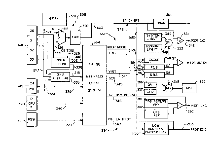
Fig. 3 illustrates a portion of the instruction unit
and storage unit affected by the present invention during
the running of an emulation program. Portions of the
instruction unit shown in Fig. 3 and also in Fig. 2 includP
the instruction platform 301 (201 in Fig. 2), the data
access control code register 319 (219 in Fig. 2), the
domain CPU status re~ister 320 (220 in Fig. 2), and the
program status word register 321 (221 in Fig. 2). The
means 303 for generating an address for use in execution of
an instruction includes general purpose registers 326, the
adder 318 and the instruction platform 301. At least one
field of the instruction is supplied on line 327 to control
selection of a general purpose register 326 for supply of a
AMDH-5464DEL/MAH
03/SJW2 100886
7~
-12-
base address to the adder 318. At least one other field of
the instruction platform 301 is supplied on line 328 to the
adder 318 for addition with the base address to generate an
operand address for supply to the effectiv~ address
register 303. The address in the effective address
register 303 is supplied on line 330 to the storage unit
shown generally by the reference numeral 331. Further, it
is passed down the instruction unit pipeline to the B-cycle
operand address register 304. The rest of the instruction
unit pipeline is not described here.
An instruction in the instruction platform 301
supplies a plurality of fields of the instruction across
line 381 to a means 332 for decoding the instruction. In
addition, control store tags across line 329 are received
from the control store in the instruction decoding means
332. In response to the instruction decode, in the means
332, control signals are supplied on lines 333 to the
instruction unit/storage unit interface logic 334. The
instruction unit~storage unit interface logic 334 is shown
in more detail in Fig. 5.
In addition, the field of the instruction supplied on
line 327 that identifies a general purpose register holding
a base address of an operand is supplied to domain storage
access detection logic 335. Control signals on line 336
from the instruction decode are also supplied to domain
storage access detection logic 335. Finally, signals from
the domain access control register 319 is supplied on line
337 to the domain storage access detection logic 335. The
domain storage access detection logic 335 is described in
more detail in Fig. 4. It generates a domain storage
access signal on line 338 for supply to the instruction
unit/storage unit interface logic 334.
AMDH~5464DEL/MAH
03/SJW2 100886
4 ~ ~L
The instruction unit/storage unit interface logic 334
in addition receives other control signals from the domain
access control register 319 across line 339. Also, the
domain CP~ status register 320 supplies control signals
5 across line 340 to the interface logic 334 and the program
status word register 321 supplies control signals on line
341 to the interface logic 334.
The interface logic 334 generates control signals that
are supplied to the storage unit 331 and used in retrieving
data in response to addresses that are supplied across line
330 from the effective address register 303. The control
signals include the address mode signal on line 342, the
system address signal on line 343, the virtual address
signal on line 344, the secondary address space signal on
15 line 345, the inhibit check key signal on line 346 and the
inhibit low address protection signal on line 347.
The address mode signal on line 342 controls the mode
of the address supplied on line 330 by determining whether
a 24-bit or a 31-bit address is supplied.
The system access signal on line 343 controls the
manner in which the storage unit responds to the address on
line 330, as either a system address or as a domain
address. When a system control program is set up, the
storage uni~ is loaded with parameters defining domain
limits in system storage int~ register 348. The address
space assigned to the system control state is also stored
as system limits in a register 349. The system limits and
domain limits are supplied to a selector 350 which is
controlled by the system access signal on line 343 to
select either the system limit or the domain limit. An
address on line 330 is compared in comparator 351 with the
selected system limit or domain limit to determine whether
a valid address has been supplied for access. If the
AMDH~5464DEL/MAH
03/SJW2 100886
~ ~,;> ~ t~ ~L
-14-
address is not a valid address, then an address exception
is generated on line 352.
In addition, the system access signal is used to
determine the kind of translation performed on the address
in the cach~. A domain address can be either a virtual
address or a real address. If it is a virtual address,
then a translation lookaside buffer 353 is used in
translation. If it is a real address, a domain base adjust
mechanism 354 is used to adjust the address to a system
address within the domain. If it is not a domain access,
then no translation or domain base adjust is necessary.
A virtual address signal on line 344 in combination
with the system address signal on line 343 is thus used to
control the mode of translation as indicated at 355.
For dual address space instructions as specified in
IBM/370 architecture, the secondary address space signal on
line 345 controls access to the primary and secondary
stores. The location of the primary and secondary address
spaces is specified in control register 1 (356), and
control register 7 (357), respectively. The secondary
address space signal on line 345 controls the selector 358
for supplying the appropriate identifier to the dynamic
address translation circuitry 359.
The inhibit key check signal on line 346 inhibits
generation of a protection exception on line 360 when the
tag access key and the user storage keys do not match as
indicated by the values stored in registers 361 and 362
respectively.
The inhibit low address protection signal on line 347
inhibits the generation of protection exception on line 363
when low address protection detection circuitry 364 detects
an address from line 330 in a low address area.
AMDH-5464DEL/MAH
03/SJW2 100886
"~
-15-
As can be seen, the storage unit receives an address
on line 330 and processes it in response to a plurality of
control signals. For each instruction that supplies an
address to the storage unit to retrieve an operand, the
system access signal on line 343 specifies whether a system
address or a domain address is being supplied. However, as
mentioned above, the instruction platform 301 contains no
field or bit to specify a system or domain access is being
made. According to the present invention, a means is
provided for generating a control code upon entry into an
emulation program that is stored in the domain access
control regIster 319 to enable implied domain addressing.
The domain storage access detection logic 335 compares the
contents of the field ~rom the instruction that specifies
the general purpose register to be used in generation of
the operand address with a preselected range of general
purpose registers to determine whether domain access is
required for certain instruction. The domain access
storage logic 335 also receives certain control signals
from the instruction decode 332 across line 336 identifying
instruction formats as described in more detail below. A
domain access control signal is supplied on line 338 to the
instruction unit storage unit interface logic 334 to
influence the generation of the system access signal on
line 343.
In addition, according to the present invention, the
domain access control register 319 stores other signals
that in combination with the control signals stored in the
- domain CPU status register 320, operate to override the
signal supplied from the program status word register 321
to the interface logic 334. These control signals
influence the generation of the address mode signal on line
342, the virtual address signal on line 344, the secondary
AMDH-5464DEL/MAH
03/SJW2 100886
7~
-16-
address signal on line 345, the inhibit check key signal on
line 346 and the inhibit low address protection key on line
347 during an access to domain address space from an
emulation program operating in control state. The features
described in the present application are described below.
C. Implied Domain Addressing
With Implied Domain Addressing, the instruction set
capable of use in accessing domain storage from Control
State is extended to include essentially all instructions
which are capable of accessing system storage. A
particular range of system GPRs 326, when they are used to
provide a base address, can optionally cause implicit
domain addressing. These registers are termed Domain
Addressing Base Registers, or DABRs.
Implied Domain Addressing is activated via DABR
Activation Control bits in the DACR 319. When Implied
Domain Addressing is active, and a Domain Addressing Base
Register is used to address an operand, Domain Addressing
is used instead of System Addressing, except for those
references which are explicitly specified as always using
System Addressing or always using Domain Addressing.
D. Domain Addressing Base Re~L__ers (DABRs).
System GPRs 2-7 are designated the Domain Addressing
Base Registers (DABRs). They operate identically to the
other system GPRs except when Implied Domain Addressing is
active, and they are specified in particular register
field(s) of an instruction. In that case, Domain
Addressing rules are followed (in performing effective
address calculations and/or accesses to main storage) for
the corresponding operands in the following cases:
- Instruction operands which are virtual addresses.
- Instruction operands which are logical addresses.
- Instruction operands which are real addresses.
AMDH-5464DEL/MAH
03/SJW2 100886
-17-
Implied Domain Addressing never applies to the
- following cases:
- Instruction addresses.
~ Addresses of PSWs, interruption codes, and associated
information used during an interruption.
- Addresses that are added by the hardware as an offset
to a base address. In this case, the base address
determines the type of addressing.
- Formation of operand addresses that are not used as
addresses.
The following table shows the register fields, for
each instruction forma~, which designate the DABRs for
addressing by each operand, in Control State when the
corresponding system GPRs are active as DABRs.
AMDH-5464DEL/MAH
03/SJW2 100886
-18-
Base Registers Used as DABRs:
DABR addr for:
Instr. Opd Opd
Type *** Instruction Format *** 1 2
+__+__+__~__+
RR / OPC /Rl/R2/ R1 R2
+__+__+ _+__+
RR / OPC /Ml/R2/ - R2
+__+ _+__+__+
RR / OPC / I
+__~__+__~__+__+__~__+__+
RS / OPC /R1/**/B2/ D2 / - B2
+__+__+__~__+__~__+__+__~
RX / OPC /**/X2/B2/ D2 / _ B2
+__+__+__+__+__+__+__~__+
S / OPC /B2/ D2 / - B2
+__+__+__+__+__+__+__+__+
SI / OPC / 12 /B1/ D1 / B1
+__+__+__+__+__+__+__+__+__+__+__+__+
SS / OPC / ** /B1/ D1 /B2/ D2 / B1 B2
+__+__+__+__+_~+__+__+__+__+__+__+__+
SSE/ OPC /B1/ D1 /B2/ D2 / B1 B2
+__+__+__+__+__+__+__+__+__+__+__+__+
RRE/ OPC / / /R1/R2/ - R2
+__+__+__+__+__+__+__+__+
E. Domain Access Controls
Domain Access Controls activate implied domain
addressing for each storage operand. Two bits are defined
to allow 2 ranges of DABRs. However, this can be
generalized to allow one control bit for each DABR.
Each control bit can be set independently, depending
on whether implied domain addressing is to be used for a
particular set of DABRs. The domain access control bits
are defined in the control word of the instruction to be
emulated and can be manipulated by control state machine
instructions.
In the fast assist mode FAM, fields of the current PSW
are overridden. Program execution is controlled by an
AMDH-5464DEL/MAH
03/SJW2 100886
, .
-19-
effective PSW. Operation is in EC mode and supervisor
state with many interruptions disabled. For system storage
accesses, 31 bit real addressing is used with program event
recording (PER) disabled. The PSW key for system storage
accesses (system key) is set by macrocode when a domain is
activated.
The effective PSW that controls domain storage
accesses in FAM is called the Domain CPU Status IDCPUS).
The DCPUS in FAM is the PSW that was in effect for the
instruction to be emulated. This PSW is captured as part
of the FAM entry routine and placed in a system register.
It specifies the user control mode and controls:
- PER for domain references as controlled by Control
Registers 9, 10, and 11.5 ~ Domain addressing relating to
- Dynamic Address Translation
- Addressing Mode
- Domain Key
- Address Space Control.
In FAM the DCPUS can be modified using a control state
defined instruction. This is equivalent to loading a new
PSW.
Domain Access Controls allow manipulation of various
bits in the PSW associated with domain storage accesses.
The facility is called Domain Access Controls. Domain
Access Controls specify override actions for certain fields
of the DCPUS and/or control registers, which would
otherwise control domain addressing, in addition to the
bits provided to control activation of the Domain Access
Base Registers (DABRs) used for implied domain addressing.
This allows the emulation routine the capability of
manipulating these functions without modifying the domain
PSW. This improves the efficiency of the emulation routine
AMDH-5464DEL/MAH
03/SJW2 100886
3~
-20-
by reducing the number of instructions required for
emulation. The Domain Access Controls are contained in the
Domain Access Control Register (DACR). The DACR is loaded
from the control word of the emulated instruction on FAM
entry, and can be modified in the emulation routine by
control state machine instructions.
DOMAIN ACCESS CONTROLS FORMAT:
0 16 /S/P/R/T/A/C/DT /~7
/ = Reserved
S = Secondary Addressing Override: Use secondary
virtual addresssing on Domain Addressing storage
references which are subject to translation (overrides
effective DCPUS S bit - treated as 1).
The setting of this control is ignored if the
efective DCPUS specified BC mode.
P = Domain Primary Addressing Override: Use primary
virtual addressing on Domain Addressing storage
references which are sub~ect to translation loverrides
effective DCPUS S bit - treated as 0).
The setting of this control is ignored if the
effective DCPUS specifies BC mode.
R = Domain PER Storage Alteration Override: Suppress
PER storage-alteration-event tests on Domain
Addressing storage references (overrides CRg bit 2 -
treated as zero).
T = Domain Translation Override~ 5uppress
translation on logical Domain Addressing storage
references (overrides effective DCPUS T bit - treated
as zero).
A = Domain Addressing Mode Override: Use 31-bit
effective addressing generation rules for domain
addresses. (Overrides effective DCPUS (A)-treated as
one). This control takes effect irrespective of
whether the effective DCPUS specifies BC mode or EC
mode.
AMDH-5464DEL/MAH
03/SJW2 100886
~ 7~
-21-
C = DABR Activation Control 1: Activate Implicit
Domain Addressing for system GPRs 4-7 as DABRs.
D = DABR Activation Control 2: Activate Implicit
Domain Addressing for system GPRs 2-3 as DABRs.
Note: Bits C and D may both be one. In that
case both designated sets of system GPRs are
active as DABRs.
L = Domain Low-Address Protection Override: Suppress
low-address protection on domain addressing storage
references (overrides CRO bit 3 - treated as 0).
K = Domain Key Protection Override: Suppress key
protection on Domain Addressing storage references
(overrides effective DCPUS KEY field, bit 8-11
treated as zeroes).
The following table summari~es the actions of the
Domain Access Controls:
EFFBCT ON DOMAIN
ADDRESSING WHEN
OVERRIDES CONTROL IS ON:
_
S - Domain Secondary Addr. Override DCPUS.S Secondary Addr.
P - Domain Primary Addr. Override DCPUS.S Primary addr.
R - Domain PER Override CR9.2 PER storage alt. off
T - Domain Translation Override DCPUS.T DAT off
A - Domain Addressing Mode Override DCPUS.A 31-bit eff. addr.
2 5 C - DABR Activation Control 1 - DABR set 1 activated
D - DABR Activation Control 2 - DABR set 2 activated
L - Domain Low-Addr-Protection Ovrrd. CRO.3 LAP off
K - Domain Xey Protection Override DCPUS.KEY Key protection off
l. The Override Controls operate as follows:
When a bit is on, the corresponding override is made
active for all Domain Addressing by the CPU in E'AM.
When a bit is off, the corresponding override action
is defeated, and Domain Addressing proceeds as usual
(under control of the DCPUS, control registers, etc.).
AMDH-5464DEL/MAH
03/SJW2 100886
-22-
2. The DABR Activation Controls control use of the DABRs
in determining whether domain addressing rules apply.
They operate as follows:
If a bit is off, the associated set of system GPRs
operate identically to the other system GPRs.
If a bit is on, the associated set of system GPRs is
acti~e as DABRs. Use of one of those system GPRs as a
base for logical or real addressing causes domain
addressing rules to be followed,
II. IMPLIBD DOMAIN ADDRESSING IMPLE~ENTATION
The logic diagram for domain storage access logic 335
is shown in Fig. 4. The logic establishes whether the
current storage access is a Domain Storage Access (DSA3.
The instruction OPCODE field D0 (D0, Dl, D2 for 2 byte
OPCODES~ is decoded in logic 432 for instruction format
types. Only RR, RRE and SS formats are decoded as
indicated by signals on lines 440, 441 and 442,
respectively. All other formats have their DABR field in
the same position. Instruction decoding is also provided
to establish whether the storage access involves the first
storage operand. This is important in cases such as SS
format instructions where there are 2 storage operands,
each having its own unique DABR. Certain RR format
instructions also have 2 storage operands. The term "OAR1
access" on line 444 indicates that the first storage
operand is being accessed. That is, Bl for SS formats and
Rl for RR formats. Since all other formats have only one
storage operand, the "OARl access" applies to either Bl or
B2 operands.
Three other functional signals are provided by the
instruction decode logic 432:
AMDH-5464DEL/MAH
03/SJW2 100886
7~.
-23-
1) DFIST on line 443 ~ indicates the first flow or
sequence of an instruction algorithm,
2) USER on line 445 - indicates that the processor is
in user state (that is - not FAM or control state),
3) DISABLE DSA on line 446 - a decode which inhibits
Domain storage access for certain instruction types
such as branch instructions which require system
addresses.
The domain access control register bits 28 on line 447
and 29 on line 448 activate implicit domain addressing for
system GPRs 4-7 and 2-3 as DABRs respectively,
Fig, 4 shows the logic implementation of domain
storage access logic having reference number 335 in Fig, 3.
The instruction platform is broken down into a plurality of
fields, D0-D4, as described above. Depending on the
format of the instruction, a particular field is used to
access a base address from a general purpose register.
Thus, either the Dl, D2 or D3 fields can be used to specify
a general purpose register, The domain storage access
logic thus includes means 449 for comparing the Dl field to
determine whether it specifies a register within the range
of 4 to 7, and a means 450 for determining whether the Dl
field is within the range of 2 to 3. These are connected
to receive the contents of the Dl field across line 451.
The contents of the D2 field are supplied across line
452 to means 453 for detecting whether D2 falls within the
range of 4 to 7 and means 454 for determining whether D2
falls within the range of 2 to 3.
The D3 field is supplied on line 455 to a means 456
for determining whether D3 falls within a range of 4 to 7
and a means 457 for determining whether D3 falls within a
range of 2 to 3. Obviously the range of general purpose
registers used for domain access base registers is
AMDH-5464DELtMAH
03/SJW2 100886
-24-
arbitrary and can be selected from any range that suits the
user.
Depending on the values of bits 28 and 29 from the
domain access control register 419, either range 4 to 7 or
2 to 3, or both, is specified as the domain address base
register range. Thus, AND-gate 458 receives as inputs bit
28 from line 447 and the output of the comparator 449 to
generate a true output when a domain address base register
from the range 4 to 7 has been specified by the field Dl.
AND-gate 459 receives as inputs the output of the
comparator 450 and the bit 29 on line 448 from the domain
access control register to generate a true output when a
domain address base register in the range 2 to 3 has been
specified by the field Dl. Likewise, AND-gate 460 receives
as inputs the output of comparator 453 and bit 28 from line
447 and AND-gate 462 receives the output of comparator 456
and bit 28 on line 447 from the domain access control
register. The output of AND-gates 460 and 462 go true when
a domain address base register in the range of 4 to 7 has
been specified by fields D2 or D3, respectively.
AND-gates 461 and 463 receive as inputs the output of
comparators 454 and 456 respectively as well as the bit 29
from the domain access control register on line 448. The
outputs of AND-gate 461 and 463 go true when a domain
address base register in the range 2 to 3 i5 specified in
the fields D2 or D3, respectivelyO
The output of AND-gates 458 and 459 are supplied to
line 471 to indicate a domain access from an instruction
format that specifies a domain address base register in
field Dl. The output of AND-gates 461 and 460 are supplied
to line 472 to indicate a domain access by an instruction
format that specifies a domain address base register for
field D2. The outputs of AND-gates 462 and 463 are
AMDH-5464DEL/MAH
03/SJW2 100~86
-25-
supplied on line 473 to indicate a domain storage access
from an instruction format that specifies a domain address
base register on field D3.
AND-gate 464 receives as inputs the RR format signal
on line 440, the Dl field domain access signal on line 471
and the OARl access signal (OARl) on line 444 which
generates a true output for a domain access on the first
operand in an RR format on line 474.
AND-gate 465 receives as inputs the RR format signal
on line 440, the invers~ of the OARl access signal on line
444, and the D2 field domain access signal on line 472.
Gate 465 generates a true output on line 474 for an RR
format instruction that specifies a domain access from the
D2 field that is not the first operand access as indicated
by the signal on line 444.
AND-gate 466 generates a true output on line 474 when
an instruction in the RRE format is supplied for the first
access from the operand address register for a domain
address from field D2 and it is not the first flow of an
instruction.
The output of AND-gate 467 generates a true output for
instructions in the SS format during the first flow of an
address from the instruction when a domain access is
requested from field D3. The output of AND-gate 467 is
supplied on line 475.
AND-gate 468 generates a true output when an
instruction in the SS format is supplied and it is not the
first address and not the first flow for a domain address
register specified from field D3.
The output of AND-gate 469 is asserted on line 474 for
instructions in the SS format for a first address from the
operand address register when it is not the first flow and
when a signal on line 476 is true.
AMDH-5464DEL/MAH
03/SJW2 100886
2~
-26-
The output of AND-gate 470 asserts a true signal on
line 474 for all instruction formats other than RR, RRE,
and SS during the first OAR1 access when a domain address
base register is specified from field D3.
The output of AND-gate 467 is supplied on line 475 to
a domain trigger latch 477 which supplies a signal on line
476 for controlling the output of AND-gate 469.
The signals on line 474 and 475 are supplied to
OR-gate 478 which generates an output on line 479.
AND-gate 480 generates the domain storage access control
signal on line 499 in response to the signal on line 479,
the inverse of the user signal on line 445 and the inverse
of the disable DSA signal on line 446.
AMDH-5464DEL/MAH
03/SJW2 100886
--27--
The design equation for DSA is as follows:
RR FORMAT & lDISABLE DSA & lUSER ~ (OARl ACCESS h [(Dl=4:7) &
DACR <28> +(Dl=2:3) 6 DACR <29>] -~ lOARI ACCESS &
~(D2=4:7~ 6 DACR <28> + (D2=2:3) & DACR <29>1)
+RRE FORMAT & lDISABLE DSA ~ lUSER & lDFIST ~ OARl ACCESS [(D2=4:7) &
DACR <28>+(D2=2:3) 6 DACR <29>]
+55 FORMAT & lDISABLE DSA & lUSER & (DFIST & OARl ACCESS & [(D3=4:7) &
DACR <28>+(D3=2:31 & DACR <29>] +
lDFIST & lOARl ACCESS & [(D3=4:7) & DACR <28>+(D3=2:3) &
DACR <29>] +
DFIST & OARl ACCESS & DOMAIN TGR) +
RR FORMAT & lRRE FORMAT & lSS FORMAT & lDISABLE DSA &
USER & OARl ACCESS & [(D3=4:7) & DACR <28> +
(D3=2:3) & DACR <29>~
The "luser" term allows domain addressing for control
state, particularly FAM.
For RR formats, the first storage operand (OAR1
ACCESS) uses the R1 field of the instruction as a DABR.
This field is contained in the D1 instruction platform
field. The term "D1=4:7" indicates that the R1 field has a
value between 4 and 7, and it is anded with the DACR bit 28
to activate a Domain Storage Access. Similarly, the
"D1=2:3" term indicates that the R1 field has a value of 2
or 3 and it is anded with DACR bit 29 for DSA activation.
AMDH-5464DEL/MAH
03/SJW2 100886
'd ~ 4
-28-
To activate a Domain Storage Access for the second
storage operand (lOAR1 ACCESS) of an RR format instruction,
the R2 address (in the D2 instruction platform field) is
used as a DABR with the D2=4:7 term anded with DACR bit 28
or the D2-2:3 term anded with DACR bit 29.
For an RRE format instruction, the R2 field is moved
to the D2 instruction platform field in the first
instruction cycle (DFIST). Therefore no storage requests
for RRE formats can be issued in this cycle. After the
first cycle (lDFIST) the storage operand access which will
be indicated by "OAR1 ACCESS" will use the D2 field as a
DABR. Therefore D2=4:7 and DACR bit 28 or D2=2:3 and DACR
bit 29 cause Domain Storage Access.
For SS format instructions, the first storage operand
¦OAR1 ACCESS) can be accessed in the first instruction flow
(DFIST). The B1 field is contained in the D3 field of the
instruction platform. Thereore, D3=4:7 is anded with DACR
bit 28 or D3=2:3 is anded with DACR bit 29 to activate
Domain Storage Access.
At the end of the first instruction flow, the D3
field is updated with B2 data and the Bl data field is
lost. A trigger called the Domain Trigger is set in this
cycle if the Domain Storage Access condition is active.
Set Domain Trigger by:
DFIST & lUSER & SS FORMAT &
[(D3=4:7) & DACR<28> ~ (D3=2:3) & DACR<29>]
~hereafter, whenever another storage access for the first
storage access occurs (OAR1 ACCESSt, a Domain Storage
Access will result if the Domain Trigger is on. For the
second operand (lOAR1 ACCESS), the B2 field is moved into
AMDH-5464DEL/MAH
031SJW2 100886
~fr~ 2
-29-
the D3 field of the instruction platform. Therefore, after
the first instruction flow (lDFIST), a Domain Storage
Access is indicated when D3=4:7 and DACR bit 28 or D3=2:3
and DACR bit 29 are active.
For all other instruction formats, only one storage
operand exists and it may be either the Bl or B2 field of
the instruction. It will reside in the D3 field of the
instruction platform. Therefore, for these formats (lRR
FORMAT & lRRE FORMAT & lSS FORMAT) when the storage access
is active (OARl ACCESS) the Domain Storage Access is
Activated by D3=4:7 and DAC~ bit 28 or D3=2:3 and DACR bit
29.
III. DOMAIN ACCESS CONTROL IMPLEMENTATION
.
The Domain Access Controls manipulate various control
signals to the storage unit. The control bits are loaded
into the Domain Access Control Register ~DACR) from the
control word o the instruction to be emulated at the
beginning of the FAM entry routine. The register can be
modiied by the "Load DACR" instruction in FAM. The
controls basically override the Domain CPU Status (DCPUS)
which is the domain or user PSW in effect at the beginning
o FAM entry. The DCPUS is loaded into system register 6.
The access signals that are impacted by the Do~ain Access
Controls are as follows:
- System (Domain)
- Virtual (Real)
- Address Mode
- Address Space
- Inhibit Key Checks
- Inhibit Low Address Protection
- Store PER
AMDH-5464DEL/~AH
03/SJ~12 100886
-30-
The logic equations presented with each signal are a
subset of the full logic equation and cnly relate to the
domain storage access portion of the logic. There are
special excepticn cases in some of the equations, indicated
by a "Force " term. This term in effect can Gverride
the DAC overrides. Th~ Domain Access Control logic is
shown in Fig. 5.
As shown in Fig. 5, the instruction platform 501
supplies a portion of the instruction across line 527 to
the instructiGn decode logic 532 (~hich correspor.ds to the
instruction decode logic 332 in Fig. 3). Instructicn
decode logic 532 generates a force system signal, a force
user signal, a force real signal and a force primary signal
across line 533 which is suppliec] to the instruction
unit/storage unit interface logic 534 !corresponding to
block 334 in Fig. 3).
~ n addition, the domain CPU status register 5,Q
supplies control signals across line 540 to the inter~ace
logic 53~. The domain access control register 5~9 supp1ies
control signals across line 541 to the interface logic 534.
The domain storage access detect,ion 1Ogic 535 qenerates the
domain storage access signal (DSA) on line 538 for supply
to the interface logic 534.
The output of the interface logic includes a system
access signal on line 543, t,he virtual signal on line 544,
the address mode signal on line 542, the secondary address
space signal on line 545, the inhibit key check signal Gn
line 546, the inhibit low add,ress protection key on line
547 and the program event recording signal (P~R) on line
520.
A~D-gates 510 and 511 make up logic generatincJ the
system access signal on line 543.
~MDH-5464DEL/MAH
Q3/SJW2 100886
2~a
~31-
AND-gate 510 receives as inputs the inverse of the
user signal, the inverse of the DSA signal, and the inverse
of the force user signal.
AND-gate 511 receives as inputs the inverse c,f the
force user signal and the force system signal. Thus, the
system access signa] on line 543 is true when the rorce
system signal is true and the force user signal is nGt
true. Further, when the force user signal is not true, if
the domain stor7ge access sign~] is not true and the user
signal is not true, then the system access signal is
asserted.
The virtual signal on line 544 is supplied at the
output of AND-gate 512. The input of AND-gate 512 includes
the inverse of the user signal, the domain storage access
signal, the domain DPU status bit-T, the inverse of the
domain access control register bit-T, and the inverse of
the force real signal.
The address ~ode signal on line 542 indicates a 31 bit
address when the output of AND-gate 513 or AND-gate 514 is
true. The input to AND-gate 513 includes the DSA signal,
the bit-A from the domain CPU status signal, and the
inverse of the user signal. The output of AND-gate 514
includes the DS~ signal, the domain access control register
bit-A, and the inverse of the user signal.
The secondary address base signal on line 545 is true
when the outputs of AND-gate 515 or AND-gate 516 are true.
The input to AND-gate 5~5 includes the bit-E of the domain
CPU status register, hit~ cf the domain access cc~trol
register, the domain storage access sign~l, the inverse of
the force primary signal and the inverse of the user
signal. The inputs to AND-gate 51fi include the inverse of
the user signa], the inverse to the force primary signal
and the domain storage access signal. In ~ddition, inputs
A~DH-5464DEL/MAH
03/SJW2 100886
-32-
include -the inverse of the bit~P of the domain CPIJ status
signal and the inverse of the output of AND-gate 521. The
input tc AND-gate 521 includes bit-E of the domain CPU
status register and bit-P of the domain access control
register.
The inhibit key check signal on line 546 is generated
at the output of AND-gate 517. The input to AND-gate 517
includes the inverse of the user signal, domain storage
access signal, and bit-K Gf the domain acce~3 contrcl
register.
The inhibit low address protection ~ignal on line 547
is supplied from the output of AND-gate 518. The input to
AND-gate 518 includes the inverse of the user signal, the
do~ai~ storage access signal, and bit-L of the domain
access control register.
The program event recording signal on line 520 is
asserted from the output of AND-gate 519. The input to
A~D-gate 519 includes the inverse of the user signal, the
domain stcrage access signal, the bit-R from the domain CPU
status register, and the inverse of bit-R from the domain
access control register.
The storage unit control signals influenced by the
DACR and the DCPUS registers are summarized as fol].ows:
A. System Access
_ _ _
This signal on line 543 indicates an acces~ to
system address space with system addresses. The signal
must be disahled for domain storage accesses.
SYSTEM = [lUSER ~ 1DSA + FORCE SYSTEM] & 1FORCE USER
In FAM, the DSA signal will disable system accesses. The
"force system" term which specifies required system access,
overrides the DSA term, and the "force user" term will
A~DH-5464DEL/MAH
03/SJW2 100886
~ 4
-33-
disable the system access. The force terms are mutually
exclusive.
B. Virtual Access
This signal on line 544 indicates that the
current storage access will require dynamic address
translation.
VIRTUAL = lUSER & DSA & DCPUS-T & lDACR-T &
lFORCE REA~.
For domain storage access in FAM the virtual signal is
under control of the DCPUS-T bit. However, the DACR-T bit
will override the DCPUS-T bit to disable virtual accesses.
The force real term will also disable virtual accesses for
specific operands which are required to access real
storage.
C. Address Mode Access
When active, this bit on line 542 indicates a 31
bit storage address otherwise a 24 bit address is implied.
ADDRESS MODE = lUSER & DSA & [DCPUS-A + DACR-A]
For domain s~orage accesses in FAM, 31 bit addressing is
active if either the DCPUS-A bit or the DACR-A bit is
active.
D. Secondary Address Space
When active, this signal on line 545 indicates
secondary address space; otherwise, primary address space
is implied.
ADDRESS SPACE = lUSER & DSA & lFORCE PRIMARY
(l[DACR-P & DCPUS-EC~ ~ lDCPVS-P + DACR-S & DCPUS-EC)
AMDH-5465DEL/MAH
03/SJW2 100886
3~
-3q-
For domain storage accesses in FAM, the address space
signal is active when the DACR-S bit is active while the
domain is in EC mode (DCPUS-EC), unless the operand storage
access r~quires a primary space access for the given
instruction (force primary3. Address space will also be
active if the DCPUS-P bit is of and either the DACP~-P bit
or the DCPUS-EC bit is off, unless again the operand
storage access requires a primary space access~
E. Inhibit Key Check
When active, this signal on line 546 inhibits
protection key checking in the storage unit.
INHIBIT KEY CHECK = lUSER & DSA & DACR-K
For domain storage accesses in FAM, protection key checking
is inhibited when the DACR-K bit is active.
F. Inhibit l,ow Address Protection
When active, this signal on line 547 inhibits low
address protection in the storage unit.
INHIBIT LAP = 1USER & DSA & DACR-L
For domain storage accesses in FAM, low address protection
checking is inhibited when the DACR-L bit is active.
G. _orage Pr~gram Event P~ecording (PER)
This signal on line 520 is not an interface
signal to the storage unit, but it is impacted by domain
storage accesses in FAM. ~n fact, the only storage PER
events that can occur in FAM are for domain storage
accesses since PER is inhibited for svstem addresses.
ENABLE STORE PER = lUSER & DSA & DCPUS-R & lDACR-R
AMDH-5464DEL/MAH
03/SJW~ 1008~6
~ 41
--3--
For domai11 s~oraqe accesses in FAM, store PE~ is under the
control of the DCPUS-R bit. ~lowever, the DACR-P ~it ~Jill
override the DCPUS-R bit to disable store PER.
IV. FAM ENTRY T~STS IMPLEMENTATION
Figs. 6 and 7 illustrate implementation of the FA~
entry tests indicated by block 223 of Fig. 2
The instr~ction emulation routines ~ust test for
program exceptions as part of normal instruction execution,
even though the program exceptions may seldom occur. To
improve the efficiency of these routines, this disclosure
provides a hardware technique which does the F,rogram
exception testing as part of the emulation entry rGutine.
The tests provide a means of indicating:
- whether s~1pervisor state is specified by the PS~
during entry to FAM for the emulated instruction.
- whether operands of the emulated instruction meet
required alignment tests.
- whether the FAM entry instruction was the target of
an execute instruction.
Each test is perfor~ed independent of the outccme of
any other test. The tests to be perforn-~ed are specified in
the control word of the instruction to be emulated. If a
FAM entry test fails, then an associated bit in a specifie~
system general purpose register (System GPR 3) is set ard
the mode of entry to F~ is nodified from fast entry to
normal entry. Tn this case, instead o~ branching to the
start of the emulation routine, the FAM entry routine would
- branch to a con~,on routine as all alternative, which
service~ program exceptions and ~pecial cases.
As illustrated in Fig. 6 the FA~ entry test logic 623
receives the code~ from the control store indicating FAM
entry tests on line 6,4. The supervisor state test signal
AMDH-5464DEL/M~H
03/SJW2 100886
-36-
is supplied to supervisor test control 630. The supervisor
test control reads sit 15 of the program status word for
the instruction to be emulated, which determir,es whether
the problem state is on. If it is on, the test failc as
indicated by a signal on line 631. The signal on line 631
is supplied to the control store branch lGgic ~4 to cause
a branch to a normal entry to process the exception
conditicn.
In addition, the FA~. entry tests perform aligrment
tests. For instructions that include a first operand,
control logic 632 for alignment of the first operar~ is
enabled. During a flow of the instruction pipeline, when
the address of the Gperand reache6 the B-Cycle operand
address register (204 in Fig. ~), Bits 29 to 31 are read to
perform the alignment tests in block 633. If the first
operand fails the alignment test, a signal is asserted on
line 631 to force the control store to normal er,try.
~ikewise, the alignment of a second operand is erab1ecl
through alignment to control 63a. When the addres~s of the
second operand reaches the B-Cyc1e operand address
register, bits ~9 through 31 are read and the test: is
performed in logic 635. If the te~t fail~, the signal cn
line 631 is asserted.
Finally, the target of execute test is perfcrmed upon
entry jnto fast emulation by checkiny an execute mGde
trigger which is set during normal operaticln ~hen an
in~truction is subject to an execute instruction as
specified by I~/370 principles of operation. If the
execute mode trigger is on during entry, the signal on line
631 is asserted to force the control store to normal entry.
Fig. 7 provides detailed implementation of the test
logic for the fast entry tests shown in Fig. 6.
AMDH-5464DEL/~H
03/SJW2 100886
d ~ d 7~
The instruct.ion control word ~ro~, the cGntrc,] store
includes a supervisor test activation ~it 701, a 4-bit
alignment test code including alignment 1, ~,;t r, al7d
alignment 1, bit 1, alignment 2, hit O and alignment 2, ~it
1. In addition, when the opcode is decoded in a decoder
704 in the instruction unit, the execute mode trigger 705
is set when the execute instruction is assert.ed.
The supervisor test logic includes AND-gate 706, which
receives a inputs the supervisor test activatic~r~ ~)lt fro~
the control word 7nl and the bit 15 from the program status
word. If both are asserted, the supervisor tect fails is
indicated by signal on line 707.
The alignment test receives as inputs the alignment 1,
Bit O and Bit ~ from block 702 of the contro~ store ar.d the
alignment 2, Bit O and ~it ~ from block 703 of the control
store which are supplied to â se1ector 708. The selector
is controlled by the alignment control logic se1.ecting
alignment 1 control words during the flow of the first.
operand address and alignment 2 control words during the
flow of the second operand address. The alignment test
control signals from the cGntrol store are decoded i.n a
decoder 709 as specified in the table below.
If the value is OG, the signal on line 710 is supplied
to AND-gate 711. ~he output of AND-gate 71~. indicates that
there is no alignment test to be performed sc the test
passes.
If the value of the selected code is 01, a signal is
supplied on line 712 as one input to AND-gate 713. The
other input to AND-gate 713 is the inverse of Bit 31 of the
operand address regi.ster and a check is performed on half
word alignment.
If the value selected to the decoder 709 is lO, then a
signal supplied on line 7~4 is one input to AND-gate 715.
AM~H-5464DEL/MAH
03/SJW2 100886
-38-
The other inputs to AND-gate 715 include Bits 30 and 31
from the operand address register. Thus, the output of
AND-gate 715 is the result of a full word alignment check.
If the value of the selected code is 11, a signal is
asserted on line 716 and supplied as one input to A~D-gate
717. The other inputs to AND-gate 7~7 include bits 29, 30
and 31 of the operand address regi,ster. Thus, a double
word alignment check is performed.
If the aliqnment test pases as indicated by the
output of any of the gates 711, 713, 715, 7~7, a ciyna1 is
asserted.
A~D-gates 719, 720 and 721 combine to set an alignmen~
test fail trigger 722. The value Gf the aligrment test
fail trigger is supplied on line 707 indicating the
alignment test has failed. The inputs to AND-gate 719
include an operand 1 test control signal indi~ating a test
of the first operand from the align~lent test, control and
the inverse of the alignment test pass signal from line
718.
The inputs to AND-gate 720 include the inverse cf the
alignment test pass signal on line 718, and an operand 2
test control signal from t,he alignment test control.
The inputs to AND-gate 72~ include the operand 2 test
control signal from the alignment test control and the
output of the alignment of the test fail trigger 722. ~'hen
the output of any of the gates 71~ through 721 is true, the
alignmen~ test ail trigger 722 is set. Signals on line
707 are supplied to OR-gate 723 so that if any of the tests
fail, a signal is supplied to fast entry logic (214 in Fig.
2), to dicable entry into the fast emulation ard require
normal entry.
AMDH-5464DEL/MAH
03/SJW2 lQ0886
-39
In addition, the failure of each of the tests is
indicated by storing a bit in a system general purpose
register 724.
A. Supervisor Test
When the function is selected for an instruction,
and the instruction is executed in User State, if the
current PSW (Problem State) is on:
- Normal entry instead of fast entry to FAM will
occur.
- System GPR3 (l) is set to one.
The supervisor test is activated by a bit in the
control word of the instruction to be emulated. This bit
is anded with PSW bit 15 (problem state), indicating a
privileged instruction being emulated in problem state, and
causes the supervisor test to fail. Fast entry is disabled
and normal entry is enabled. Macrocode will emulate the
instructiGn according to the environment through -the normal
entry routine rather than executing the emulated
instruction~ Macrocode knows that the supervisor test
failed because the hardware/microcode stored the results of
the supervisor test in bit 1 of system GPR3.
B. ~ nment Test
A model may provide for alignment tests on
specific operands of specific instructions. If the
function is available and selected for an instruction
operand, a 2-bit code specified by control store fields
determines the type of alignment test to make on the
instruction operands. The possible code values and test
types are:
AMDH-5464DEL/MAH
03/SJW2 100886
I
.
q-P~
~~o-
VALUE TEST
/ 00 / No check
/ 01 / Half word ali~nment check
/ 10 _ ! Full word alignment check L
~ Double word a1~gnment check/
If a fast entry instruction fails the alignment test:
- A normal entry instead of fast entry tG FP~ will
Gccur .
- System GPR3 (0) is set to one.
The alignment test for one or two instruction operands
is activated by two bits per operarld in the cGntrol wGrd of
the instruction to be emulated. The proper activation bits
are selected when the assocjated low order 3 bits of the
storage operand address are available. The operand
alignment test is used for all instruction formats except
RR and SS formats. The operand 2 alignment test is used
for the second storage operand of R~ or SS format
instructions to be e~ulated. The selected 2 bit activation
code is decoded and gated with the associated o~erand
address register (OAR) bit(s) to be tested. A 0p code
indicates no alignment test. A 01 code will test operand
address bit 31 [OAR 31). If it is a one, the alignment
test will fail. A ~0 will test operand add~ess bi~s 30 and
31. If either hit i~ a one, the aliynment test will fail.
Finally a 11 code will test operand address bits ~, 3Q,
and 31. If any bit is a one, the alignment test will fail.
In the case of instructions with two storage opeIarlds
to be emulated, the results of the first test is held in ar~
"alignment test fail" trigger while the second o~erarld
address is being tested (if activated). I~ either operand
A~DH-5464DEL/MAH
03/SJW2 100886
~ ~ ~33 ~tj~ ~
-41-
fails the alignment test, fast entry will be disabled and
normal entry will b~ taken. ~acrocode will emulate the
instruction acccrding to the environment through th~ ncrmal
entry routine rather than executing Lhe instruction. The
alignment test failure will cause bit 0 of system ~7PR3 to
be set.
C. Target of Execute Test
GPR3(2) will be set to 1 if the FAM entry instruction
was the target of an ~XECUT~ instruction. If the FAM entry
instruction wGuld otherwise cause a fast entry to FA~, the
entry mode is changed to normal.
~ acrocode must know when emulating an instruct;on
whether the instruction ;s a targ~:t of an execute
instruction. During the normal processing of an execute
instruction, the hardware sets an ~eY~ecute ~Gdel~ trigger
indicating that the subject instruction is a target of an
execute. If this trigger is on during FAM entry, fact
entry will be disabled and normal entry wil] be taken, and
bit of system GPR3 will he set.
V. CONCLUSION
Firmware emulation of new instructions using existing
machine instruetions provides an ~ffeetive way of
introdueing r.ew functions or features without modifying
existing maehine hardware. These functions or features are
implemented on a higher level than ~icroeode or hardware
control points, and provide greater flexibility. This
class of firmware is ealled macroeode and the instruction
emulation is called fast assist.
The present invention improves instruction emulation
routines by:
1) Providing hardware ascist mechanisms which
perform many oi the emulation routine tests, thereby
AMDH-5464DEL/MAH
03/SJ~2 100886
-42-
reducing the number of cycles of execution for each
emulation routine.
2) ~efining a cGntrol technique which can manipulate
accesses to program storage, thereby reducinc~ the number of
instructions required for each emulation routine.
3) Providing a mechanism for making any machine
instruction have the capability to make storage accessc-~ to
program storage as well as emulation storage, thereby
reducing the number of instructions required for each
emulation routine.
The invention has been described with reference to a
particular embodiment. Those skilled in the art will
recognize that many variations and mc)difications c,f the
embodiment described can be made that fall within the
spirit of the invention. The scope of the inventior is
meant to be defined by the following claims.
AMDH-5464DEL/MAH
03/SJW2 100886