Note : Les descriptions sont présentées dans la langue officielle dans laquelle elles ont été soumises.
i34
- 1 - 20104-8303
The invention relates to a method of manufacturing an
optical stripline waveguide for non-reciprocal optical components,
in which a a monocrystalline waveguide strip with a refractive
index n2, which is surrounded by material with a lower refractive
index nl, is provided on a monocrystalline substrate.
In optical transmission lines light is conducted either
in optical waveguides in the form of optical fibres or in planar
waveguides which are constructed as stripline waveguides with a
refractive index stop towards smaller values in the material sur-
rounding the waveguide strips. With respect to this matter,
reference is made to R.G. Hunsperger, "Integrated Optics" : ThQory
and Technology, Springer-Verlag, 1982, in particular pp. 38-69.
The planar stripline waveguides can be constructed as strip-loaded
waveguides, page 43, ridged waveguides, page 66 or channel wave-
guides, page 38. These embodiments are determined inter alia by
the present state of the art.
The present metho~ is particularly suitable for the
manufacture of ridged waveguides and channel waveguides as well
as for the manufacture of semi-leaky optical isolators. In the
case of semi-leaky isolators the forward wave of the incoming
light passes the isolator without attenuation (for example TM-
mode), whereas reflected waves are leaked out (formation of TE-
modes).
The known stripline waveguides are produced with
materials which have so far been used in integrated optics, such
as LiNbO3, or on the basis of AIIIBV compounds. In particular for
.,", ~
129~634
- 2 - 20104-8303
non-reciprocal optical waveguides the use of iron garnet has
proved to be particularly suitable. So far it has not been pos-
sible to manufacture stripline waveguides on the basis of iron
garnet in a quality which satisfies the requirements.
Planar iron garnet waveguides are envisaged, for ex-
ample, as optical isolators in coherent transmission networks at
frequencies >102 MHz; in this respect, reference is made to I.E.E.E.
J. Quantum Electro. QE-18, 1982, page 1975, A channel waveguide
must satisfy the following requirements: waveguide strips should
optlmally have the thicknesses of a few ~m. In order to permit
waveguide strip thicknesses of a few ~m, the step size value of
the refractive index n2-nl relative to the material surrounding the
waveguide strips must be in the order of some 10 3 when a single-
mode propagation is to be attained in the stripline waveguide. When
the step size value of the refractive index between the material of
the waveguide strip (n2) and the surrounding material (nl) is so
low the light wave will leak deeply into the surrounding material,
so that in order to obtain small losses in the waveguide strip not
only the waveguide strip itself but also the surroun~ing material
must exhibit a very low degree of intrinsic absorption ~ and a very
low degree of light scattering (< 1 dB/cm).
It is an object of the invention to provide a method
by means of which stripline waveguides and in particular semi-
leaky optical isolators can be manufactured on the basis of iron
garnet, which exhibit a low degree of intrinsic absorption ~ and
have adjustable values of the refractive index step n2-nl in com-
'~
63~
- 3 - 20104-8303
bination with limited other losses.
This object is achieved according to the invention,
which comprises a method of manufacturing an optical stripline
waveguide for non-reciprocal optical components comprising the
steps of providing a crystallographically oriented substrate, form-
ing a first monocrystalline iron garnet layer on said substrate by
RF cathode scattering in an inert gas plasma using a target of
mainly an iron garnet phase together with other phases of almost
equal sputtering rate, said first layer having a first index of
refraction n1, epitaxially growing a monocrystalline waveguide
strip material on said first layer by RF cathode sputtering with
said target, said waveguide strip having a second index of refrac-
tion n2, where n2 > nl, locally disturbing the lattice structure
of the surface free of said waveguide strip to form a lattice
disorder, and surrounding said waveguide strip with iron garnet
material having said first index of refraction n1. Apart from
the iron garnet phase there may also be other phases, for example
orthoferrite or Fe2O3.
The invention is based on the recognition that sputter
epitaxy of, for example, complex layers which consist of elements
having a very different sputtering rate can be carried out when
monocrystalline substrates having well-defined, undisturbed sur-
faces and targets having phases with an almost equal sputtering
rate are used, and when the RF cathode sputtering process is car-
ried out in an inert gas plasma, preferably a helium group gas
plasma, making use of preferably a magnetron electrode.
1291634
- 3a ~ 20104-~303
According to further advantages embodiments of the
method according to the invention, a (lll)-oriented non-magnetic
garnet single crystal disc is used as a substrate, or a (110)-
oriented non-magnetic garnet single-crystal disc is used as a
substrate; preferably, the single-crystal discs consist of calcium
magnesium zirconium-substituted gadolinium gallium garnet
(Gd,Ca)3(Ga, Mg,Zr)5O12. However, other non-magnetic gallium
garnet substrates may be used as well. In particular the use of
a (llO)-oriented garnet single crystal disc provides the possibil-
ity of producing an optical isolator having a strain-induced
optical bi-refringence in the (plane of the) layer. By means of
twin-crystal-rocking-X-ray curves it has been found that the mono-
crystalline layers deposited on such a substrate have a satisfac-
tory X-ra~ line width, even when there is a high crystal lattice
misfit of approximately 1% between the substrate and the deposited
monocrystalline layer, which is interesting for isolators having
semi-leaky properties.
According to a further advantageous embodiment of the
inventive method, the monocrystalline waveguide strip and the
material surrounding it have a composition according to the general
formula ~A/B)3(A,B)5O12, where A = at least one rare earth metal,
Bi,Pb and/or Ca and B = Ga,Al,Fe,Co,Ni,Mn,Ru,Ir,In and/or Sc.
'~,,
~29~4
PHD 87.033 4 5.5.1987
Unlike, for example, liquid phase epitaxy
processes, the sputter epitaxy process is carried out in a
state of thermochemical non-equilibrium, consequently the
manufacture of, for example, garnet layers in non-
5 equilibrium compositions is possible without using aforeign phase,
For example, single-phase iron garnet material in
the form of monocrystalline waveguide strips and differently
ordered (amorphous or polycrystalline) material surroundi-g
them of the following compositions were manufactured:
1. Gdl 90Bi1 45Fe4,09Alo~34Gaot22o12
d1 ,97Bi1 ,o4Fe4 51GaO 22A1o 2612-
According to further advantageous embodiments ofthe inventive method, the material which late~lly
surrounds the waveguide strip is amorphous or poly-
crystalline. Polycrystalline material is to be preferred
when low degrees of absorption are required.
According to advantageous embodiments of the
20 method according to the invention, the substrate is heated
in the epitaxy process to a temperature which is higher
than the temperature at which epitaxial growth on substrate
regions having an undisturbed crystal lattice starts,
and which is lower than the temperature at which poly-
25 crystalline growth on substrate regions having adisturbed crystal lattice starts; prefereably~ the sub-
strate is heatecl to a temperature in the range from 450
to 520C.
Accorcling to a further advantageous embodiment of
30 the inventive method, the subs~te heated in the epitaxy
process to a temperature which is higher than the
temperature at which polycrystalline growth on substrate
regions having a disturbed crystal lattice starts;
preferably, the substrate is heated to a temperature of
> ~20C.
At temperatures over 450C it becomes possible
to deposit a layer consisting of regions of different order,
namely amorphous or polycrystalline layer regions and mono-
1291634
PHD 87.033 5 5.5,1987
crystalline garnet layer regions, on a monocrystallinegarnet substrate having a locally disturbed lattice
structure. The substrate temperature to be selected depends
upon the desired composition of the layer to be formed and
upon its order, and it must be established empirically.
In a sputter epitaxy process the substrate
temperature during the deposition process plays a part:
a higher substrate temperature favours a spontaneous
crystallization of the deposited layer; in this respect it
was found that epitaxial growth on substrate regions
having an undisturbed crystal lattice starts at lower
temperatures than polycrystalline growth on substrate
regions having a disturbed crystal lattice. In other
w rds, epitaxial growth < polycrystalline growth-
Hereina~ter these temperatures will be designated Tepi
and Tpoly, respectively. When substrates are used whose
crystal lattices were at the surface locally converted to
a condition of disorder, for example by an iron bombard-
ment, an amorphous or dependent on the substrate tempera-
ture, a polycrystalline layer is deposited on the
disturbed substrate regions by the cathode sputtering
process, whereas on the undist~rbed, monocrystalline
regions the material deposited by cathode sputtering grows
as a monocrystalline layer. In other words, the substrate
temperatùre T for the manufacture by means of sputter
epitaxy of a structured layer having monocrystalline and,
next thereto~ amorphous layer regions is to be selected
so that: Tepi ~ TSubstrate ~ poly
The substrate temperature T for the manufacture
of monocrystalline waveguide strips with, next thereto,
polycrystalline material must be selected so that :
substrate > Tpoly. When the substrate is heated to a
temperature below that at which epitaxial growth starts,
only amorphous layers are deposited, independent of whether
the substrate has a disturbed or an undisturbed crystal
lattice.
~3~
PHD 87.033 6 5.5.1987
In the manufacture of stripline waveguides on
the basis of iron garnet by means of RF-cathode sputtering,
it has been found that the iron garnet material .grows in
a monocrystalline manner on monocrystalline garnet
5 substrates when the substrates are heated to a temperature
450C.
When layers on the basis of iron garnet are
deposited on substrates which are not monocrystalline in,
at least, near-surface regions such as, for example,
disturbed monocrystalline or amorphous substrates,
amorphous to X-ray amorphous layer~ are formed at a sub-
strate temperature below approximately 520C, and
polycrystalline layers are formed at substrate temperature
> 520C,
According to an advantageous embodiment of the
inventive method, the deposition of the waveguide-strip
forming material is preceded by the deposition of a mono-
crystalline iron garnet layer of the same material by means
of RF cathode sputtering, which layer is provided with a
20 refractive index n1 which is lower than the refractive
index n2 of the waveguide strip because in comparison with
the conditions under which the monocrystalline waveguide
strip is deposited a higher RF voltage is applied to the
target electrode and/or the pressure of the inert gas
25 plasma is increased and/or the substrate temperature
is raised and/or an RF voltage 6(substrate bias) is applied
to the substrate electrode.
According to an advantageous further embodiment
of the inventive method, the deposition of the material
30 forming the waveguide strip is followed by the deposition of
a further iron garnet layer of the same material by means
of RF cathode sputtering, which layer grows in a monocrystal-
line manner on the waveguide strip and in an amorphous or
polycrystalline manner on the material which laterally
35 surrounds this strip, and which layer is provided with a
refractive index n1 which is lower than the refractive
inde~ n2 of the waveguide strip, because in comparison with
129~.~;3~
PHD 87.033 7 5.5.1987
the conditions under which the monocrystalline waveguide
strip is deposited a higher RF voltage is applied to the
target electrode and/or the pressure of the inert gas plasma
is increased and/or the substrate temperature is raised
5 and/or an RF voltage tsubstrate bias) is applied to the
substrate electrode.
According to a further advantageous embodiment
of the inventive method, the material which laterally
surrounds the waveguide strip is removed in a subsequent
10 etching step, and by means of RF cathode sputtering a
further monocrystalline iron garnet layer of the material
forming the waveguide strip is deposited next to and on the
waveguide strip, which is provided with a refractive index
nl which is lower than the refractive index n2 of the
15 waveguide strip because an inert gas plasma is used having
a pressure, preferably in the range from 0 2 to 2.0 Pa at
an iron energy from approximately 10 to 102 eV, which is
higher than that of the inert gas plasma used to deposit the
waveguide strip. A lower refractive index nl of the further
20 monocrystalline iron garnet layer can also beobtained by
raising the RF voltage which is applied to the target
electrode or by raising the substrate temperature or by
applying a RF voltage (substrate bias) to the substrate
electrode. All four measures lead to an increase of the
25 selective back-sputtering rate of the elements involved
in the formation of the layer and having very low sputtering
rates (for example bismuth). ~9 the etohing rate of
amorphous iron garnet material in~ for example, a chemical
etching process in H3P04 and at a temperature of 150C
30 is approximately 5 times that of monocrystalline iron garnet
material, and ths etching rate of a non magnetic gadolinium
garnet substrate is a factor of two lower than that of
monocrystalline iron garnet, the material surrounding the
monocrystalline waveguide strips in the form of amorphous
35 iron garnet can be quantitatively removed without damaging
the monocrystalline waveguide strips. As described above,
the mono-crystalline waveguide strips must be surrounded by
129~634
PHD 87.O33 8 5.5.1987
material having a refractive index which is lower for
the desired mode of the incoming-light and~ in the case
of a semi-leaky optical isolator, higher for the modes
which are complementary to the desired mode. This can be
5 obtained by depositing the further monocrystalline iron
garnet layer after the amorphous material surrounding the
monocrystalline waveguide strips has been removed.
Dependent upon the height of the pressure of the
inert gas plasma maintained during the epitaxial deposi-
10 tion, the particle bombardment of the growing layer takesplace at a reduced and varying intensity, which leads to a
modification of small back-sputtering effects. A lower
pressure of the inert gas plasma leads to a lesser particle
bombardment of the growing layer due to the h~her plasma
15 density, and to a more uniform composition of the
deposited target layer. If the pressure of the inert gas
plasma is slightly decreased, the composition of the
deposited layer changes due to the decrease in particle
bombardment. This phenomenon is used to deposit in an
20 epitaxial manner iron garnet material which due to the back-
sputtering effects has a slightly different composition~
and hence, different refractive indices n2 or n1. In the
case of magnetron-sputtering these effects are more
conspicuous only in the amorphous iron garnet, because
25 apparently the surface binding energy of certain components
is less than in crystalline material.
According to advantageous embodimentsofthe
inventi~e method, a monocrystalline cobalt-substituted
iron garnet layer is deposited as an absorbing layer,
30 preferably by means of liquid phase epitaxy, on the single
crystal disc which forms the substrate, or an amorphous
iron garnet layer whose composlti~n corresponds to that of
the waveguide strip is deposited as an absorbing layer on
the further iron garnet layer by means of RF cathode
sputtering, to which layer a refractive index n3 is
imparted which is equally high or higher than the
refractive index n1 of the further iron garnet layer,
1291634
PHD 87.033 9 5.5.1987
because in comparison with the conditions under which the
further iron garnet layer is deposited a lower inert gas
plasma pressure is applied, preferably in the range from
0.1 to 1 Pa, and/or a lower subs~ate temperature is used,
5 pre--erably in the range from 200 to 450C. The proper
functioning of single-mode waveguides renders imperative
the suppression of undesired modes. The material which
acts as an absorber does not have to fully surround
the stripline waveguide, it is sufficient when an
lO absorbing layer is provided over or underneath the layer
structure which forms the stripline waveguide.
According to advantageou~ embodiments of the
inventive method, the monocrystalline waveguide strip
and the material surrounding it are deposited in an inert
l5 gas plasma having a pressure from 0.2 to 2.0 Pa, and the
further iron garnet layer is deposited in an inert gas
plasma of the same pressure range, yet at a pressure which
is higher than the pressure used to deposit the waveguide
~trip.
According to a further adva~tageous embodiment
of the inventive method, the lattice structure of the
substrate in the form of a Barnet single crystal disc or
the lattice structure of the monocrystalline absorbing
layer provided on an undisturbed garnet single crystal disc
25 or the lattice structure of a first monocrystalline iron
garnet layer provided on an undisturbed monocrystalline ab-
sorbing layer is disturbed to a depth of a few atom
layers by an ion bombardement from an inert gas plasma
in the regions on which no waveg-uide strip should grow in
30 an epitaxial manner. A sputter-etching process(iron bombard-
ment from the plasma) at relatively low RF voltages and
relatively low sputtering gas pressures can suitably be used
to so disturb the lattice structure of a monocrystalline
substrate, which is to be coated epitaxially by means of
35 cathode sputtering, in near-surface regions to a depth of
only a few atom layers that dependent upon the substrate
temperature instead of a monocrystalline layer a layer of
12~ ;3~
PHD 87,O33 lO 5.5.1987
different order, pre~erably an amorphous or polycrystalline
layer, is grown on the disturbed regions, next to
a monocrystalline layer on the undisturbed regions of
the substra~e. This has the advantage that the same
5 arrangement can be used during the entire process, and that
a sufficient lattice imperfection is obtained with a depth
of only a few atom layers. Preferably, the regions which
are not to be disturbed by ion bombardment are covered
with a photoresist mask, after which the ion bombardment
lO is carried out in a helium-group gas plasma at a pressure
from O.l to 1 Pa and an ion energy > 3O eV.
According to a further advantageous embodiment
of the inventive method, a magnetron is used as a target
electrode, to which the RF power necessary for the sputte-
15 ring process is applied. The use of a magnetron resu~in a concentration of the plasma near the target, and
consequently in a substantial reduction of the ion
bombardment of the ~rowing layer, so that, for example,
the layer will not be subject to back-sputtering effects
20 which adversely affect the epitaxial growth, When a
magnetron electrode is used, a maximum concentration of
the plasma near the target can be obta:ined b~ selecting a
phase composition for the target to be sputtered which
exhibits the smallest possible saturation magnetization. The
25 use of a magnetron has the addltional advantage that in
comparison with methods which employ R~ cathode ~puttering
devices in a diode arrangement, the distance between target
and substrate can be optimized, i.e. the lowest possible
plasma density and smallest possible amount of kinetic
30 energy in the vicinity of the substrate in combination
with the highest possible deposition rate.
~ ccording to an advantageous embodiment of the
inventive method the system consisting of a substrate,
a monocrystalline waveguide strip and amorphous material
35 surrounding the latter is subjected to a tempering process
at a temperature at which lateral epitaxial growth takes
place from the sides of the waveguide strip to the
1291634
PHD ~7.O33 11 5.5.1987
amorphous material surrounding it, such that along the
sides of the waveguide strip a monocrystalline cladding
having a thickness of several/um is formed. Also in this
way monocrystalline waveguide strips are obtained having
5 steep, homogeneous, smooth and abrupt interfaces with the
surrounding amorphous material.
Advantageously, the tempering process is carried
out within a temperature range of about 5O K below the
crystallization temperature of the amorphous material.
lO Thus, the value of the absorption ~1 of the amorphous
iron garnet material approaches the absorption ~2 of the
monocrystalline iron garnet material, which in the case
of a lightwave leaking into the stripline waveguide leads
to a reduction of the propagation losses. Due to the simi-
5 larlty in the composition of the amorphous layer therefractive index is graded in conformity with the crystal-
lized material.
The method according to the invention provides
the following advantages:
The present method permits the manufacture in
one production cycle and by means of an epitaxial deposi-
tion procoss of optical stripline waveguides, in particular
of the buried channel waveguide type having isolating
properties, in which the stripline waveguides obtained
25 are homogeneous through the entire cross-section
regarding structure, refractive index and magnetical proper-
ties; they exhibit a high geometric resolution, and
in particular smooth, steep interfaces between mono-
crystalline material and ma-terial of a different order,
30 (amorphous or polycrystalline).
In the wavelength range over 1/um the
interface between amorphous and monocrystalline ranges
exhibits a refractive index st0p which can be set towards
smaller values thanks to the present method and which is
necessary to propagate the waves in monocrystalline wave-
guide strips. The intrinsic absorption ~ of the mono-
crystalline iron garnet produced by RF cathode sputtering
1;~91~3~
PHD 87.033 12 5.5,19~7
is very low in the wavelength range over 1/um; by means of
a propagation method a total loss ~ of ~ 0.15 cm was
measured in the plane of the layer at a wavelength of 1.33
/um, which loss includes the leakage of the planar
waveguide. The interface between amorphous and monocrystalli-
ne material is very smooth and steep, which also in the
waveguide strip leads to a low degree of leakage. The
geometric resolution of the structures formed with the
present method is of the order of < + 1.5/um.
A further advantage of the present method is
that apart from material of different order (amorphous or
polycrystalline) a single arrangement can be employed
for the manufacture in one production ~ycle of mono-
crystalline waveguide strips, said arrangement being
15 used both for the preparation of the substrates to be
coated (ion bombardment) and for the manufacture of the
iron garnet layers, which from the point of view of
efficiency is important in a manufacturing process.
A further advantage of the present method is
that, in contrast to the liquid phase epitaxy, very thin
homogeneous layers can be manufactured without
transition layers being formed.
Yet another advantage of the present method is,
for example, that for the manufacture of iron garnet layers
25 on a non-magnetic substrate, matching the lattice con9tants
of the substrate and the layer is easier than in the case
of~ for example~ liquid phase epitaxy; lattice mismatches
> 1~ are acceptable. Such mismatches are even required
when optical isolator concepts having semi-leaky proper-
ties have to be obtained.
RF cathode spl~tering can be carried out by means
of commercially available RF voltage-operated cathode
sputtering devices having a target c~hode (magnetron)
which is provided with a magnetic system and which has a
diameter of for example 7.6 cm, a device for measuring
the effective RF voltage both at the target electrode and
the substrate electrode having to be provided. The magnetron
129~L634
PHD 87.033 13 5.5.1987
cathode is provided vertically in an ordinary vacuum
recipient. An RF generator supplies the RF power
necessary for the sputtering process to the target
electrode and the substrate electrode through impedance
matching elements, and subsequently to the plasma. The
stabilization of the RF voltage on the target electrode
at values smaller than ~ 1~ is obtained via a computer
control. The pressure of the sputtering gas is also kept
constant to + 1 /c by a computer control. An ordinary RF
generator is used as an energy source for the sputtering
arrangement, which generator is operated at an output
power of 200 W. The operating frequency is 13.56 M~Iz.
The invention will now be explained in more
detail by means of exemplary embodiments.
Figures la to 1c show types of stripline
waveguides according to the present state of the art;
Figure 2 is a diagram of refractive indices of
the materials used in a stripline waveguide according to
the invention,
Figure 3 is a diagram of the intrinsic absorp-
tion ~ of the materials used in a stripline waveæuide
according to the invention;
Figures 4 to 7 are sectional views of strip-
line waveguides according to the invention.
Figures 1a to 1c are schematic sectional views
of types of stripline waveguides according to the
present state of the art (Figure 1a: strip-loaded waveguide,
Figure 1b: ridged waveguide, Figure 1c: channel waveguide).
WL denotes the waveguide strip, S denotes the sub-
strate. The stripline waveguides shown are made of mate-
rials having refractive indices n1, n2 and n3, where
n ~ n ~ n~.
3 ~ 2
Figure 2 depicts the refractive index n of
monocrystalline (circles) and amorphous (triangles)
bismuth-substituted gadolinium iron garnet which is
deposited in situ, a part of the iron being substituted
by aluminium and gallium, as a function of the wavelength
~ (/um) and the photon energy h~ (ev).
i3~
PHD 87.033 14 . 5.5.1987
The Figure shows that the interface between
amorphous and monocrystalline material in the for the
stripline waveguide relevant wavelength range over 1/um
e~hibits a refractive index step towards ~a~er values,
5 as is required for propagating waves in monocrystalline wave-
guide strips. According to the present method said
re.fractive index step can be adjusted, i.e. it can also be
reduced to very small values as is required in the case of
single-mode waveguides having a greater thickness.
Figure 3 depicts the intrinsic absorption
(l/cm) of monocrystalline and amorphous bismuth-
substituted gadolinium iron garnet which is deposited in
situ, a part of the iron being substituted by aluminium and
gallium, as a function of the wavelength ~ (/um) and the
photon energy h~ (eV). In the Figure the following ~ta
are plotted in succession from the bottom to the top
a monocrystalline material (growth temperature 520C),
the same material after it has been tempered for half an
hour at 690 C, 660C and 550C, and an amorphous material
(deposition temperature 360C). From the Figure it becomes
apparent that the degree of intrinsic absorption cC of the
monocrystalline iron garnet material manufactured by means
of RF cathode sputtering is very low in the for the use
of the waveguide relevant wavelength range over 1/um.
The amorphous iron garnet, however, has a degree of
absorption which allows it to be used as an absorbing layer
to suppress undesired modes. Moreover, the absorption ~ 1
of the amorphous iron garnet material can be approached in
the present method by tempering at a temperature which is
close to the crystallization temperature of the absorption
~ 2 of the monocrystalline material~ which is important
for the manufacture of low-loss stripline waveguides of
the channel waveguid~ type.
By way of e~ample, a description is given of
the manufacture of stripline waveguides for non-reciprocal
optical components, having monocrystalline waveguide strips,
and the material surrounding them which is of different
~6~
PHD 87.033 15 5.5.1987
order and which consists of bismuth-substituted gadolinium
iron garnet, a part of the iron being sub--tituted by
aluminium and gallium.
In ( 111 )-direction or (110)-direction oriented
5 calcium magnesium zirconium~substituted gadolinium gallium
garnet single crystal discs 1 having a diameter of 30 mm
were used as substrates, which discs were pretreated in known
manner before the deposition process, such that epitaxial
growth can take place. A first monocrystalline layer 5
lO (see Figures 4-6) of bismuth-substituted gadolinium iron
garnet is deposited on these substrates by means of RF
cathode sputtering, a part of the iron being substituted
by aluminium and gallium. This iron garnet layer 5 is
deposited by means of the same target as that which
l5 is used for the later manufacture of monocrystalline wave-
guide strips 9g and the material 97 surrounding them.
A refractive index nl is imparted to this first iron garnet
layer 5 by a suitable selection of the sputtering parameters,
which refractive index n1 is lower than the refractive
20 index n2 of the monocrystalline waveguide strip
materlal to be deposited afterwards on this iron garnet
layer because in comparison with the conditions under which
the monocrystalline waveguide strip is deposited a higher
RF voltage is applied to the target electrode and/or the
25 pressure of the inert gas plasma i9 increased and/or the
substrate temperature is raised and/or an RF voltage
(substrate bias) is applied to the substrate electrode. To
deposit the first monocrystalline iron garnet layer 5,
a helium-group gas, preferably argon, having a pressure of
30 o.6 Pa is introduced into the sputtering equipment
which is evacuated to a pressure of ~ 10 5. Such a layer
having a refractive index nl smaller than that of the
waveguide strip to be provided next is required to obtain
single mode propagation in the strip-line waveguide to be
35 manufactured. A pressure difference of the inert gas plasma
of, for example, approximately 0.5 Pa leads to a refractive
index step of approximately 5.10 3. In order to produce
~L291634
P~D 87.033 16 5.5.1987
a l~cally disturbed la-ttice structure, the areas o~ the
substrate on which the waveguide strip is to grow
epitaxially and whose lattice structure is consequently
not to be disturbed are subsequently provided, or before
the first epitaxial iron garnet layer 5 is applied, with
a photoresist mask, and the substrate is subjected to an
ion bombardment in a helium-group gas plasma having a
pressure from 0.1 to 1 Pa, preferably 0.2 Pa, at an ion
energy of > 30eV, preferably some 10 eV. Subsequently the
photoresist mask is removed. The other parameters of the
method correspond to those which will be described herein-
after with respect to the manufacture of monocrystalline
wav0guide strips and the material surrounding them.
A body of iron garnet mixed oxides which is
manufactured by hot pressing or sintering is used as a
target (cathodic sputtering source), said body having a
diameter of 7.5 cm, a thickness of 4 mm, a porosity of
< 10~ and, preferably, a saturation magnetization Ms f
~ 25 G.
In the following examples of embodiments
powdered mixtures of BiFeO3, Gd2Bi1Fe5012,Al203 and Ga203
are sintered in an oxygen atmosphere having a pressure of
1 bar for 6 hours at a temperature C 920C, the process
being conducted so that there is substantially no residual
free Bi203 in the ceramic structure. Free Bi203 must not
be present in the target because it will lead to mechanical
disintegration of the surface of the target due to the fact
that it has a higher sputtering rate than the other target
constituents; thanks to the use of mixed oxides a homoge-
nization of the sputtering rate of all phase constitutents
of the target is obtained.
Examvle I
For the manufacture of monocrystalline single-
phase iron garnet waveguide strips and the amorphous
material surrounding them of the composition
Gd1~90Bi1~45Fe4,ogAlo~34 GaO 22l? a target having a
diameter of 7,5 cm and of the following composition is
129~634
PHD 87.033 17 5.5.1987
used (quantities in % by weight):
Gd23 33.64
Bi23 31.80
5 Fe203 31.52
2 3 ' 5
Ga23 1.89
The target body is attached to the target
electrode by means of a satisfactorily heat-conducting
lO adhesive (for example epoxy resin filled with silver
power).
In order to conduct away dissipated heat it is
efficacious to use, for example, water-cooled target
electrodes.
The deposition process is conducted so that the
sputtering equipment is first evacuated by means of a
vacuum p~p to a pressure ~ 10 3 Pa, after which a helium-
group gas, preferably argon, having a pressure of o.6 Pa is
introduced. The distance between the target and the sub-
20 strate is 80mm. The depositi~n rate is approximately 0.8
/um/h. The RF voltage measured at the RF supply lead on the
rear side of the target electrode is 230 Vr ; the substrate
voltage is floating. The substrate temperature is 480C.
Example II
For the manufacture of monocrystalline single-
phase iron garnet waveguide strips and the amorphous
material surrounding them of the composition
1,97 1 ~o4Fe4~51Gao~22Alo 2612 a target having a
diameter of 7.5 cm and of the following composition is used
30 (quantities in /0 by weight):
Z03 36.514
~i23 24,122
Fe23 36, o74
Al23 1.220
35 Ga203 2, 070
As described with respect to Example I~ the
target bod~ is attached to the target electrode. It is
also efflciacious to use water-cooled target electrodes to
1291~34
PIID ~7.O33 18 5.5.1987
conduct away dissipated heat. The coating process is
carried out as described with respect to E~ample I,
however, the substrate temperature was 510C.
Before the layers are deposited (typical layer
5 thicknesses are from 1 to 5/um) the target is pre-etched
by an ion bombardment from the plasma until the target
material thus removed has a constant composition. In
further experiments with the same target the pre-etching time
is reduced from approximately 5 h to some 1Om, until the
l0 equilibrium potential has stabilized at the target.
After deposition in the cathode-sputtering
device, layers are obtained which are amorphous, X-ray
amorphous or polycrystalline on the substrate regions with
a lattice disorder, and which are mono!crysta~ine on the
15 substrate regions with a monocrystalline, undisturbed
crystal lattice.
Figures 4, 5, 6 and 7 schematically show strip-
line waveguide structures as they are produced according
to the present method.
In Figure 4 a cobalt-substituted iron garnet
layer 3 is first provided on a non-magnetic, (110)-
oriented gadolinium gallium garnet substrate 1, preferably
by liquid phase epita~y; said layer 3 prevents the
development of higher wavemodes, caused by a higher degree of
25 absorption~ at the interface with the substrate. As has been
stated above~ the proper functioning of single-mode
waveguides requires the suppression of undesired modes,
the stripline waveguide not having to be completely
surrounded by the absorbing material. As an alternative to
30 the above-mentioned cobalt_substituted monocrystalline
iron garnet layer, an amorphous iron garnet absorbing layer
produced by means of RF cathode sputtering may be used,
which layer is provided over the stripline waveguide
structure (see Figure 7).
As described above, the first monocrystalline iron
garnet layer 5 is then provided by means of RF cathode
sputtering. As described above, the thus prepared substrate
129~
PHD 87.033 19 5.5-1987
', 3, 5 is disturbed by ion bombardment in the near-
surface lattice regions; in Figure 4 these regions are
indicated by reference numeral 7, in the later deposition
process an iron garnet layer 9 with amorphous or poly-
crystalline regions 97 is gro~n on these regions. In the
later deposition process, iron garnet is grown in a
monocrystalline manner in the non-disturbed lattice regions
of the layer 5, thereby forming a waveguide strip 99.
Subsequently, a further iron garnet layer 11 is deposited
also by means of RF cathode sputtering using the same
target as for the manufacture of the waveguide strip 99 and
the amorphous or polycrystalline regions 97, which iron
garnet layer grows in a monocrystalline manner in the
region 119 over the waveguide strip 99 and in an amorphous
or pDlycrystalline manner in the regions 117 over the
amorphous or polycrystalline regions 97. This further iron
garnet layer 11 is provided with a lower refractive index
n1 than the iron garnet layer 9 because in comparison
with the manufacturing conditions of the iron garnet layer
9, for the deposition of the iron garnet layer 11 either
a h~her RF voltage is applied to the target electrode,
the inert gas plasma pressure is increased, the substrate
temperature is higher or an RF voltage (substrate bias),
for example 25 Vrms, is applied to the substrate
electrode. In the present example, an lnert gas plasma
pressure of 1.0 Pa and a substrate temperature in the range
from 480 to 540C were used to deposit the further iron
garnet layer 11. At a substrate temperature o4 480C the
iron garnet layer 11 grows amorphously in the regions 117,
at a substrate temperature > 540C this iron garnet layer
grows in a polycrystalline manner in the regions 117.
Figure 5 shows a part of a further embodiment
of a stripline waveguide manufactured according to the
inventive method. Up to the manufacture of the layer 9 the
process steps are the same as described with respect to
Figure 4; as shown in F~re 4 the layer 9 has a mono
crystalline waveguide strip 99 and next thereto, for example,
12916~A
PHD 87.033 20 5.5.1987
amorphous regions 97. The system th-us cbtained which
comprises the substrate 1,3,5 and the layer 9 i9 etched in
a subsequent chemical etching process in H3P04 at a
temperature of ~150C, in which process the amorphous
layer portions 97 are removed and the waveguide
strip 99 remains in tact due to the etding rate which is
approximately a factor of five lower than that of the
amorphous material of the layer portions 97. On the
structure thus obtained comprising substrate 1, 3, 5 and
monocrystalline waveguide strip 99 the further mono-
crystalline iron garnet layer 11, as described with respect
to Figure 4, is provided in a subsequent process step
by means of RF cathode sputtering.
A semi-leaky optical isolator (as described
in I.E.E.E. J. Quantum Electro. OE-18, 1982,
page 1975) which exhibits single-mode propagation is
obtained, for example, when the monocrystalline waveguide
strip 99 has a cros~section 2 3,5x3,5/um at a refractive
index step n2-n1 ~ 5.10 for the mode in question,
whereas for the mode to be leaked out the refractive index
step n2-n1 must be ~ O. In order tc arrive at low propaga-
tion losses in theisolator, the value of the intrinsic
absorption ~1 of the material surrounding the waveguide
strip must approach the small intrinsic absorption value
C~2 of the material of the monocrystalline waveguide
strip 99, and the interface between the monocrystalline
waveguide strip 99 and the material surrounding it must be
very smooth. The absorption values OC1~ ~2 of the
materials of the monocrystalline waveguide strip 99 and the
further monocrystalline layer11 are almost the same.
The necessary refractive index step n2-n1 ~
5.10 3 of the mode in question can be obtained by means of
different substrate temperatures during the deposition
process of the monocrystalline stripline waveguide 99 and
the further monoc~ystalline layer 11; a change in the sub-
strate temperature ~ T = 50 K leads to 9 for example, a
change in the lattice constants a2 of the waveguide strip
lZ9163A
PHD 87.033 21 5.5.1987
99 with respect to the lattice constants a1 f the
substrate layer 5 of 4 a l ~ 0.001 nm, which leads to
a value ~ n l ~ 5,10 due to a change in the
crystal lattice mismatch. The change in the refractive
index can mainly be attributed, however, to the ensuing
change in the bismuth content of the layer. This change
in the refractive index is approximately 10 3.
The refractive indices n2 of the material of
the waveguide strip 99 and n1 of the material of the
further monocrystalline layer 11 can be coarsely adjusted
by applying a voltage (substrate-bias) in the range fro-n
20 to 30 Vrms to the substrate elebtrode; in this way,
values of ~ n ~ 10 to 10 are obtained. When the
stripline waveguide according to the invention is
employed as a semi-leaky optical isolator the required
refractive index step n2-n1 C 0 of the modes to be
leaked out is obtained in that the waveguide strip is at
least partly surrounded by material of non-monocrystalline
order or in that the waveguide strip is at least partly
surrounded by material of monocrystalline order having a
crystal lattice constant similar to that of the material of
the stripline waveguide.
In the case of the stripline waveguide of
Figure 4, the refractive index step n2-n1 is adjusted
as described with respect to Figure 5, As the material of
the monocrystalline waveguide strip 9g has an absorption
value ~ 2 which differs from the value ~1 of the
amorphous material of the regions 97 surrounding it, ~ 1
and ~2 must be equalized. This can be achieved in a
tempering process after deposition of the material for the
waveguide strip 99 and the material surrounding it of the
regions 97, according to the diagram plotted in Figure 3.
Figure 6 shows a portion of a further stripline
wave~ide manufactured according to the inventive method.
As described above, the first monocrystalline iron garnet
layer 5 is provided by means of RF cathode sputtering on
a non-magnetic, (111)-oriented gadolinium gallium garnet
substrate 1.
lZ9~634
PHD 87.O33 22 5.5.1987
The thus prepared substrate 1,5 is, as
described above, disturbed :near surface lattice
regions by ion bombardment. Subsequently, the iron garnet
layer 9 with the amorphous regions 97 and the waveguide
strip 99 which is grown in a monocrystalline manner on the
undisturbed regions of the substrate 1,5 are deposited,
as described abo~e, by means of RF cathode sputtering.
In a subsequent tempering process at a temperature just
below the crystallization temperature of the amorphous
material of the regions 97, monocrystalline border zones
in the form of a cladding g8 are formed at the interface
between the monocrystalline waveguide strip 99 and the
adjacent amorphous material of the regions 97 by epitaxial
growth on the sides of the monocrystalline waveguide strip
99. The tempering process is continued until the cladding
9~, which grows in a monocrystalline manner, has obtained
the desired thickness. The refractive index n1 of the
cladding 98 is lower than the refractive index n2 of the
monocrystalline waveguide strip 99; the reason for this
20 is, that as the amorphous regions have less surface
binding energy they are subject to a higher degree of back-
sputtering of elements with a very low sputtering rate (for
example bismuth), and consequently their composition
slightly differs from that of the material of the mono-
crystalline waveguide strips 99. This after-treatment by
tempering may alternatively be carried out after a further
thick~ amorphous iron garnet layer 11 (for example having
a thickness of 5/um) has been deposited on the iron garnet
layer 9, such that a monocrystalline region having a
30 refractive index similar to the refractive index n1 of the
layer 5 but smaller than the refractive index n2 of the
waveguide strip 99 is formed over the waveguide strip 99.
Due to the fact that only the region of the amorphous
further iron garnet layer 11 which is situated over the
35 waveguide strip 99 has a monocrystalline order after the
tempering process, the remaining regions of the further
iron garnet layer 11 which are situated over the regions 97
~gi634
PHD 87.033 23 5.~.1987
of the iron garnet layer 9 can act as absorbers.
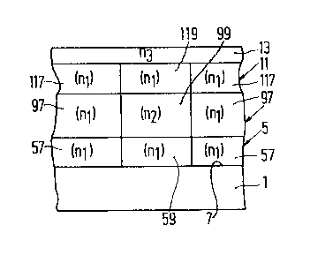
Figure 7 shows a further stripline waveguide
manufactured according to the present method. The lattice
structure of a non-magnetic, (110) - oriented gadolinium
gallium garnet single crystal disc 1 was disturbed in
the regions 7 to a depth of several atom layers by an
iron bo~nbardment in an ar~on plasma at a pressure 0.2 Pa
and an ion ener~y of some 10 2 :eV, in which process
the regions of the single crystal disc which were not to be
disturbed by the ion bombardment were masked by means of
a photosensitive layer. After the removal of the photo-
sensitive layer the first iron garnet layer 5 was provided
in a continuous production cycle by means of cathode
sputtering, which layer will grow in an amorphous or
lS polycrystalline manner in the regions 57 and in a mono-
crystalline manner in the region 59. The process parameters
~elating to the fabrication of the iron garnet layer 5
have been described hereinbefore with reference to the
Figures 4 to 6. Subsequently, the iron garnet layer 9
having amorphous or polycrystalline regions 97 and the
monocrystalline region which forms the waveguide strip
99~ and the further iron garnet layer 11 having
amorphous or polycrystalline regions 117 and a mono-
crystalline region 119 as described hereinbefore, are
provided, After deposition of the further iron garnet
layer 11 an amorphous iron garnet layer whose composition
corresponds to that of the waveguide strip 99 is deposited
as an absorbing layer to which a refractive index n3 is
imparted which is equal or higher than the refractive
index n1 of the further iron garnet layer 11, because
in comparison with the conditions under which the further
iron garnet layer 11 is deposited, a lower pressure of the
inert gas plasma and a lower substrate temperature are
applied, The amorphous absorbing layer 13 is deposited at
a pressure of 0.2 Pa and a substrate tempe~ture of 250C.
In order to obtain a semi-leaky structure for
a semi-leaky optical isolator, the following measures are
1291634
PHD ~7.O33 24 5,5.1987
.
taken: the waveguide strip 99 is deposited epitaxially
on the region 59 of the iron garnet layer 5 to obtain
the optical birefrigence which is necessary for
the proper functioning of a semi-lea~y optical isolator
by selecting the free lattice constants a of the substrate
1 and the layer region 59 so that they are different from
the free lattice constants a of the waveguide strip 99.
Preferably, the free lattice constant a of the waveguide
strip 99 is larger than the free lattice constant a of
the substrates On the other hand, the lattice of at
least one region adjacent to the waveguide strip 99,
for example the regions 97 or the region 119, should be
isolated from the waveguide strip 99, i.e. such regions
should not be deposited epitaxially in order not to produce
birefrigence there in. In this case, the requirement is
met that at the interfaces between the waveguide strip 99
and the regions 97 or between the waveguide strip 99 and
the region 119 the refractive index for the mode employed,
for example the TM mode, is lower in the regions 97 and/or
the region 119 than in the waveguide strip 99, whereas for
the leady mode, for example the TE mode, the refractive
index is higher in the regions 97 and/or 119. These
conditions can be fulfilled because with the present
method not only epitaxial regions but also regions of a
different order, for example amorphous or polycrystalline,
can be produced simultaneously.