Note : Les descriptions sont présentées dans la langue officielle dans laquelle elles ont été soumises.
~ ~9~8ZZ
--1--
TITLE OF THE INVENTION
METHOD AND APPARATUS FOR PROC~SSING AN IMAGE SIGNAL
r
BACKGROUND OF THE INVENTION
Field of the Invention
The present invention relates to an apparatus for
processing an image signal which is used to encode and/or
decode a binary image signal.
Description of the Prior Art
According to a conventionally known apparatus for
processing an image signal, an image such as a document,
diagram, or the like is scanned and read by an image
scanner to obtain an image signal. This image signal is
binarized and urther converted into a highly efficient
compressed code data by way of a two-dimensional encoding
system using, for example, the correlation between
adjacent lines. This compressed code data is then
transmitted or stored.
Such a conventional image signal processing
apparatus needs a circuit for compression encoding the
binary image signal and a circuit for decoding the
compression encoded image signal into the binary image
signal, respectively.
In the case where the two-dimensional encoding
system is used, during encoding and decoding the
reference line information, namely, the position
information at the transition (i.e., change) positions
where the value of the binary data in the preceding
adjacent line changes from black to white or from white
to black must be encoded and decoded. This is a great
amount of information and, therefore, line memories, each
having a capacity large enough so that all of the binary
image data of at least one of the reference lines can be
stored, are needed for the encoding circuit and decoding
circuit, respectively. Thus, the circuit scale and cost
q~
--2--
extremely increase as the complexity and detail of the
image increase-
There is also the problem that it takes a longprocessing time period for the step of detecting the
position information of the transition positions from the
binary image data written in the line memory.
Hitherto, in the encoding, the information
indicative of the position of the transition pixel having
a value different from the value of the pixel just before
the transition pixel of the binary signal, namely, the
address of the transition position, is detected by
checking the pixels dot by dot to see if the pixel's
value changes from white to black or from black to white
or not.
However, to check the pixels dot by dot, if it is
assumed that the time period of, e.g., 100 nsec is needed
to check one dot, takes 0.8 second to check the
transition position of the image data of one screen which
consists of, e.g., one mega bytes. Consequently, if the
processing time period for encoding after the detection
of the transition is included, a few seconds are required
to encode the image signal of one screen.
Furthermore, in the case of reproducing the image by
decoding the binary image signal from the signal encoded
as described above, the run length of the decoded line is
calculated on the basis of the code word while using the
information of the reference line. The binary image
signal is generated on the basis of the run length
calculated and the image is reproduced.
According to the conventional image signal
processing apparatus, the circuit to generate the binary
image signal based on the run length is constituted by a
counter of, e.g., twelve bitsO The run length is set to
the 12-bit counter and counted down in response to a
clock pulse which is supplied to a clock terminal.~ When
the value of the counter becomes 0, a transition signal
82~
--3--
indicative of the change from black to white or from
white to black~ris generated in the binary image signal.
In such a construction, similarly to the encoding
circuit, when it is assumed that a duration of one clock
pulse is, e.g., 100 nsec, it takes the time period of 0.8
seconds to generate the binary signal if the image data
of one screen consists of, e.g., one mega bytes. If the
time period necessary for the decoding process is
included, a few seconds are required to reproduce the
image of one screen.
OBJECTS AND SUMMARY OF THE INVENTION
It is therefore an object of the present invention
to provide an apparatus for processing an image signal
which can solve the foregoing conventional problems.
Another object of the invention is to provide an
apparatus for processing an image signal in which the
circuit scale is reduced.
Another object of the invention is to provide an
image signal processing apparatus in which the processing
time is reduced by reducing the encoding and decoding
times.
Still another object o~ the invention is to provide
a cheap image signal processing apparatus.
Still another object of the invention is to provide
an image signal processing apparatus in which at least
parts of an encoding circuit and a decoding circuit are
commonly used.
Still another object of the invention is to provide
an image signal processing apparatus which can cope with
the change of the encoding system without largely
changing the hardware.
According to one aspect of the present invention,
the above and other objects are achieved by an apparatus,
and the method embodied therein, for processing an image
signal comprising data input/output circuit means for
8Z~:
--4--
receiving input image data or compressed code data and
for outputting ~he compressed code data or output image
data, encoding circuit means for encoding the input image
data into the compressed code data, and decoding circuit
means for decoding the compressed code data into the
image data to be outputted.
Control means are provided for controlling the
encoding circuit means and decoding circuit means,
including memory means for storing a program for
controlling the encoding circuit means and a program for
controlling the decoding circuit means. Also provided is
selecting means for selecting one of the programs so as
to selectively effect encoding or decoding in the
encoding circuit means or the decoding circuit means so
that the data input/output circuit means selectively
receives the input image data or outputs the output image
data and selectively outputs the compressed code data or
output image data.
According to another embodiment of the invention,
there is provided an apparatus for processing an image
signal comprising data input circuit means for receiving
input image data having first and second binary values,
encoding circuit means for encoding the input image data
into compressed code data, and data output circuit means
for outputting the compressed code data. The encoding
circuit means includes
(i) first detecting circuit means for detecting
transition points where the value of the input image data
changes from one to another of the first and second
binary values,
(ii) counter means for generating addresses of the
transition points of the input image data,
(iii) second detecting circuit means for detecting
if the value of the input image data does not change
during a time period exceeding a predetermined period,
~9~
-
--5--
(iv) control means for controlling the counter means
so as to count~rat a faster than normal speed to a
predetermined number during each predetermined period,
when the value of the input image data does not change
during a period exceeding a predetermined period, and
(v) encoder means for encoding the input image data
by using the addresses of the transition points of the
input image data.
According to still another aspect of the invention,
there is provided an apparatus for processing an image
signal comprising data input circuit means for receiving
input image data, encoding circuit means for encoding the
input image data into compressed code data by using the
correlation between a preceding line as a reference line
and an encoding line, and data output circuit means for
outputting the compressed code data. The encoding circuit
means includes
(i) detecting circuit means for detecting transition
points where the value of the input image data changes
from one to another of the first and second binary values
and for generating information data according to the
transition points,
(ii) first and second memory means for storing the
information data,
(iii) control means for contr~olling the first and
the second memory means so that while one of the first
and the second memory means is in a write status, the
other is in a read status and the write and read statuses
are alternately changed for every line,
(iv) switching means for selectively connecting the
data input circuit means to either of the first and
second memory means, and
(v) encoder means for reading out the information
data according to the transition points of a preceding
line from one of the first and second memory means and
writing the information data according to the transition
--6--
points of an encoding line into another of the first and
second memory ~eans.
According to still another aspect of the invention,
there is provided an apparatus for processing an image
signal comprising data input circuit means for receiving
compressed code data, decoding circuit means for decoding
the input compressed code data into output image data to
be outputted, and data output circuit means for
outputting output image data.
The decoding circuit means includes
(i) counter means for presetting a,run length of the ''
input compressed code data,
(ii) detecting circuit means for detecting if the
run length of the input compressed code data exceeds a
predetermined number,
(iii) control means for controlling the counter
means so as to count at a faster than normal speed when
the run length of the input compressed code data exceeds
a predetermined number, and
(iv) decoder means for generating binary image data
according to the run length preset in the counter means.
The above and other objects, features and advantages
of the present invention will be more apparent from the
following detailed description in conjunction with the
accompanying drawings.
BRIEF DESCRIPTION OF THE DRAWINGS
Figs. lA to lC are schematic diagrams for explaining
the encoding system for use in an apparatus for
processing an image signal according to an embodiment of
the present invention;
Fig. 2 is a block diagram showing an image signal
processing apparatus according to an embodiment of the
invention; ,
Fig. 3 is a block diagram showing a transition
~ ~:9~.~322
position detecting circuit in an embodiment of the image
signal processipg apparatus according to the invention;
Fig~ 4 is a block diagram showing a memory circuit
in an embodiment of the image signal processing apparatus
according to the invention;
Figs. 5, 6A, and 6B are schematic diagrams for
explaining an embodiment of the image signal processing
apparatus according to the invention; and
Fig. 7 is a block diagram showing a decoding circuit
in an embodiment of the image signal processing apparatus
according to the invention. ..
DESCRIPTION OF T~E PREFERRED EM3ODIMENTS
An embodiment of the present invention will now be
described hereinbelow with reference to the drawings.
The two-dimensional encoding system using the
correlation between the adjacent lines, for example, the
MR (Modified Read) encoding system is used as the
encoding system for use in an apparatus for processing an
image signal according to the invention.
According to the MR encoding system, the encoding is
executed in the following procedure.
In Figs. lA to lC, blank square portions denote
white pixels and hatched square portions indicate black
pixels. The starting pixel and transition pixel for
encoding are defined as follows.
Starting pixel: The pixel of the encoding line which
becomes the starting point for
encoding and this pixel is indicated
by aO.
Transition pixel: The pixel just after the value
changed from white to black or from
black to white. The transition
pixels on the encoding line are
sequentially indicated by al and a2
The transition pixels on
9~
--8--
- the reference line are represented by
! r bl and b2-
(Procedure 1)
The pass mode is first detected. The pass mode
denotes the case (merge) where the white or black
portions (bl to b2) which appeared in the reference line
disappear in the encoding line as shown in Fig. lB. When
the pass mode is detected, the pass mode "0001" is
generated. The starting pixel aO is shifted to aO' just
under b2 (Fig. lB).
(Procedure 2)
In the case where the mode is not the pass mode, a
check is made to see if the absolute value of lal bll is
largex than three or not, thereby determining whether the
encoding is carried out in the horizontal mode or
vertical mode. If lal bll > 3, the encoding is performed
in the horizontal mode and if lal bll S 3, the encoding
is executed in the vertical~mode (Fig. lC).
In the horizontal mode, the encoding is performed in
the case (new start) where there is a weak correlation
between the encoding line and the reference line and
white or black is newly generated on the encoding line.
In the horizontal mode, the distances aO al and al a2 are
encoded using the MH (Modified Huffman) code subsequent
to "001" indicative of the horizontal mode. At the same
time, the starting pixel is shifted to a2.
In the vertical mode, the encoding is performed in
the case where there is strong correlation between the
encoding line and the reference line and it is performed
on the basis of the following table. At the same time,
the starting pixel is shifted to al.
-- lX9~8~
g
Encoding !Encoding pixel Symbol Code word
mode r
Pass mode (bl b2) _ 0001
Horizontal aO al, al a2 H 001 + M(aO al)
mode + M ( al a2 )
_ _
~,= O al bl = 1 V(O) 1 .
al bl = 1 VR( 1 ) 011
mode~ > O al bl = 2 vR(2) COOOll
al bl = 3 VR(3) 0000011
al bl = 1 VL(l) 010
~> O al bl = 2 VL(2) 000010
al bl = 3 VL(3) 0000010
The process in the case of encoding a binary image
signal will now be described.
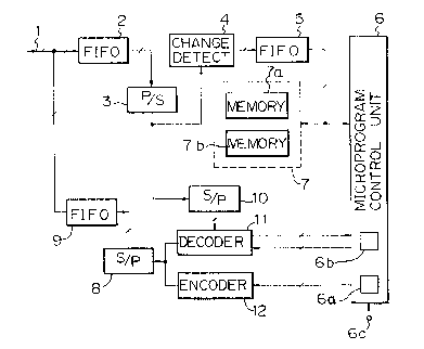
Fig. 2 shows a block diagram of an image signal
processing apparatus in which at least parts of encoding
circuit and decoding circuit are commonly used. The
image such as document, diagram, or the like which was
read by an image scanner (not shown) is converted into
binary values representative of black and white to obtain
a binary image signal. This binary image signal is
transferred as input data through an input/output (I/O)
data bus 1. The image data encoded by the foregoing
two-dimensional encoding system is also transferred as
output data through the I/O data bus 1.
In the case of decoding, the encoded image data is
transferred as input data through the I/O data bus 1 and
the binary image signal is transferred as output data
through I/O data bus 1 in a manner opposite to the case
of encoding.
The binary image signal transferred through the I/O
data bus 1 is transferred as 16-bit parallel data.
~-~9~
--10--
Namely, the binary image signal of the pixels, which are
continuously a~ranged, is divided for every sixteen
pixels, for instance. The binary image signals each
consisting of sixteen pixels are arranged to form the
16-bit parallel data. This parallel data is transferred
through the data bus 1 into a first-in first~out register
(hereinafter, abbreviated as an FIFO) 2.
An output of the FIFo 2 is supplied to a
parallel-to-serial (P/S) converting circuit 3, by which
the input parallel data is converted into serial data.
Thus, the binary image signal of each pixel is
sequentially outputted from the P/S converter 3.
An output of the P/S converter 3 is supplied to a
change (or transition) position detecting circuit 4,
which will be explained in detail later. The detecting
circuit 4 serves to obtain the transition position on the
line where the value of the binary image signal of each
pixel which is sequentially outputted changes from black
to white or from white to black.
The transition position information on the line
obtained is set to, e.g., 12-bit parallel data and
supplied through a FIFO 5 to a microprogram control unit
(hereinafter, abbreviated as an MPU) ~ and to a memory
circuit 7.
The memory circuit 7 is constituted by two memories
7a and 7b as will be explained in detail hereinbelow.
Read and write statuses o the memories 7a and 7b are
alternately switched for every line. Namely, the
transition position information of the preceding line is
stored in one memory. When this memory has the read
status, the other memory has the write status, so that
the transition position information on the current line
is written into the other memory. The transition
position information of the preceding line necessary for
the MR encoding is obtained from one memory having the
read status of the memory circuit 7. This position
8~
information is supplied to the MPU 6. The transition
position infor~ation of the current line necessary for
the MR encoding is supplied from the FIFo 5 to the MPU 6.
The encoding mode and the white run length and black
run length which are necessary for encoding are
calculated by the MPU 6 on the basis of the transition
position information of the current line and of the
preceding line. The calculated data is the parallel data
of, e.g., twelve bits and is supplied from the MPU 6 to
an encoding circuit 12.
The encoding circuit 12 is constituted by, e.g., a r
ROM and the code word based on the MR code corresponding
to the calculated data which is supplied from the MPU 6
is preliminarily written into a table. The calculated
data from the MPU 6 is converted into the code word by
the encoding circuit 12 due to the MR encoding system.
This code word is outputted as serial data from the
encoding circuit 12.
An output of the encoding circuit 12 is supplied to
a serial-to-parallel (S/P) converting circuit 8, by which
the serial data is converted into parallel data of, e.g.,
sixteen bits. This encoded data is inputted into a FIFO
9 and transferred from the FIFO 9 through the I/O data
bus 1.
The process in the case of decoding will now be
described. The image data encoded by the MR encoding
system is set to 16-bit parallel data and supplied into
the FIFO 2 through the data bus 1. The output of the
FIFO 2 is supplied to the P/S converter 3.
The 16-bit parallel data is converted into serial
data by the P/S converter 3 and this serial data is
supplied to a serial-to-parallel (S/P) converting circuit
10 .
The S/P converter 10 is constituted by a shift
register. The serial data supplied to the S/P converter
,9~2~
10 is converted to parallel data for every code word and
supplied to a ~ecoding circuit 11.
The decoding circuit 11 is constituted by a decoding
ROM to discriminate the mcde and obtain the run length
from the MX code and a signal generating circuit to
generate the binary image signal on the basis of the run
length, which will be explained in detail later. The code
word supplied to the decoding circuit 11 is inputted to
the decoding ROM of the decoding circuit 11, by which the
mode is discriminated.
The positio~ information of the change points, i.e.,
the transition points of the reference line is written in
one memory 7a or 7b constituting the memory circuit 7.
When the pass mode is discriminated, the mode information
is supplied from the decoding circuit 11 to the MPU 6.
The new starting pixel aO' is set to the MPU 6 on the
basis of the transition position information of the
reference line which has been stored in the memory
circuit 7.
When the horizontal mode is discriminated, the run
length is obtained from the MH code in the decoding ROM.
The binary image signal is generated from the signal
generating circuit of the decoding circuit 11 on the
basis of the run length. At the same time, the
transition position information of the change points
where the value of the binary image signal changes from
white to black or from black to white is written into the
other memory 7b or 7a of the memory circuit 7 through the
MPU 6.
When the vertical mode is discriminated, the run
length is calculated on the basis of the position
information of the reference line which is read out from
one memory 7a or 7b of the memory circuit 7. ~he binary
image signal is generated from the signal generating
circuit of the decoding circuit 11 on the basis of the
run length. At the same time, the transition position
- ~9~22
-13-
information of the change points where the value of the
binary image s~gnal changes from white to black or from
black to white is written into the other memory of the
memory circuit 7 through the MPU 6.
The binary image signal generated from the signal
generating circuit of the decoding circuit 11 is supplied
to the S/P converter 8 and converted into 16-bit parallel
data and then supplied to the FIFo 9. The binary image
signal which is outputted from the FIFO 9 is transmitted
through the data bus 1, so that the image is reproduced
by the binary image signal.
Although the MR encoding system has been used as the
encoding system in the above description, the M2R
encoding system, which is the extended MR system, or
other compression encoding system may also be used.
According to ~he above construction, the
input/output buffers, memories to store the information
of the reference line, and the like are commonly used in
the encoding and decoding circuits, so that the overall
circuit scale can be reduced and the apparatus can be
cheaply constituted. On the other hand, the programs
regarding the encoding and decGding are stored in
microprogram memories 6a and 6b in the MPU 6,
respectively. The encoding and decoding modes are
switched by a control signal which is supplied to a
control terminal 6c. Even when the encoding system or
the like is changed as well, there is no need to
remarkably change the hardware but it can be realized
merely by changing the program.
The change detecting circuit 4 will now be further
described in detail with reference to Fig. 3.
As mentioned above, the binary image signal
transmitted through the I/0 bus 1 is supplied to the FIFO
2 on a block unit basis, in which one block consists of
sixteen pixels. The output of the FIFO 2 is supplied to
the P/S converter 3. A clock signal is supplied from a
9~82~
-14-
terminal 13 to the P/S converting circuit 3, by which the
parallel data ~ the binary imaye signal is converted
into the serial data. At the same time, the output of
the FIFo 2 is supplied to an all black detecting circuit
14B and an all white detecting circuit 14W. The data of
the LSB tleast significant bits) corresponding to the
sixteenth data with respect to the time sequence among
the data of sixteen pixels from the FIFO 2 is latched
into a latch circuit 15.
The all black detecting circuit 14B detects whether
,the output of the FI~O 2 including the last pixel data of
the preceding block which has been latched in the latch
circuit 15 is the data of all black pixels or not. The
all white detecting circuit 14W detects whether the
output of the FIFO 2 including the last pixel data of the
preceding block which has been latched in the latch
circuit 15 is the data of all white pixels or not.
The discrimination regarding whether the data is for
all black pixels or for all white pixels in the all black
detecting circuit 14B and all white detecting circuit
14W, respectively, is executed by detecting not only the
data of the FIFO 2 but also the LS~ of the output of the
FIFO 2 of the preceding block which has been latched in
the latch circuit 15. The reason for this double
detection is to prevent malfunction in the case where the
transition of the value of the binary image signal which
is transmitted as the parallel data occurs between
adjacent two data. Namely, there is the case where the
transition occurs between the adjacent data and the value
of the pixel of the LSB of the output data of the FIFO 2
of the preceding block differs from the value of the
pixel of the MSB tmost significant bit) of the output
data of the FIFO 2 of the current block. Also the output
data of the FIFO 2 of the current block is the data,of
all black or white pixels. In such a case, if the ;,
detection is made without including the pixel of the LSB
~ ~9~32~
-15-
of the FIFO 2 of the preceding block, the 12-bit counter
will have been~counted up by sixteen, so that the
transition which occurs between the adjacent data cannot
be detected.
The output of the P/S converter 3 is supplied to a
change (or transition) detecting circuit 16. A clock
signal is supplied from the terminal 13 to the change
detecting circuit 16. The detecting circuit 16 detects
the change, i.e., transition position where the value of
the binary image signal as the serial data which is
outputted from the P/S converter 3 changes from black to
white or from white to black. An output of t~e change
detecting circuit 16 is supplied as a count enable signal
to a 4-bit counter 17a constituting a 12-bit counter 17.
A carry output of the counter 17a is supplied as a count
enable signal to a 4-bit counter 17b through an OR gate
18. A carry output of the counter 17b is supplied as a
count enable signal to a 4-bit counter 17c. By cascade
connecting the 4-bit counters 17a, 17b, and 17c in this
manner, the 12-bit counter 17 is constituted as a whole.
A clock signal is supplied from the terminal 13 to
the counters 17a, 17b, and 17c, so that the 12-bit
counter is counted up one by one. When the transition is
detected by the change detecting circuit 16, the counting
operation of the counter 17a is stopped.
The outputs of the all black detecting circuit 14B
and all white detecting circuit 14W are supplied to an OR
gate 19. When the output data of the FIFO 2 including
the output data of the latch circuit 15 is the data of
all black pixels or all white pixels, a high level signal
is outputted from the OR gate 19 and supplied as a count
enable signal to the counter 17b through the OR gate 18.
At the same time, the output of the OR gate 19
transmitted through the OR gate 18, is supplied to a
control circuit 20, so that the counting operation of the
counter 17a is stopped in response to an output of the
-16-
con~rol circuit 20. Conse~uently, the 12-bit counter 17
is counted up by sixteen at a time in response to one
clock pulse. The output of the control circuit 20 is
supplied to the FIFO 2 and the timing of the output of
the FIFO 2 is controlled.
As described above, the counter 17 is counted up by
sixteen at a time in response to one clock pulse when the
values of the data of sixteen or more continuous pixels
do not change and at the same time, when the output data
of the FIFO 2 including the data of the LSB of the output
of the FIFO 2 of the preceding block is the data of all
black pixels or all white pixels. In the case where some
of the values of the pixel data within sixteen continuous
pixels change and both of the data of white pixels and
the data of black pixels are included in the output of
the FIFO 2, the counter 17 is counted up one by one in
response to one clock pulse. At the same time, when the
transition is detected by the change detecting circuit
16, the counting operation of the 12-bit counter 17 is
stopped and the transition position on the line can be
obtained from this value.
According to the above construction, for example,
when the values of sixteen pixels of the binary image
signal do not change, the 12-bit counter 17 constituted
by, e.g., 4-bit counters 17a, 17b, and 17c is counted up
by sixteen in response to one clock pulse. Thus, the
transition position on the line can be detected at a high
speed.
The memory circuit 7 in the embodiment will now be
described in detail with reference to Fig. 4.
In Fig. 4, a line pulse is supplied to a clock input
terminal CK of a D-type flip-flop 22 from a terminal 21.
An output Q of the flip-flop 22 is supplied to one input
terminal of each of AND gates 23a and 23d and an output Q
is supplied to one input terminal of AND gates 2~b and
23c and to a data input terminal D of the flip-flop 22.
- ~?~8~Z
A low-level read pulse is supplied from a terminal 26R
through an inv~rter 25R to the other input terminals of
the AND gates 23a and 23c. A low-level write pulse is
supplied from a terminal 26W through an inverter 25W to
the other input terminals of the AND gates 23b and 23d.
The read pulse and write pulse which are supplied to the
terminals 26R and 26W are generated from the MPU 6.
Outputs of the AND gates 23a and 23b are
supplied to an NOR gate 24a. An output of the NOR gate
24a is supplied to a chip selection terminal CS of the
memory 7a. Outputs of the AND gates 23c and 23d are
supplied to an NOP gate 24b. An output of the
NOR gate 24b is supplied to a chip selection terminal CS
of the memory 7b. The write pulse is supplied to write
enable terminals WE of the memories 7a and 7b from the
terminal 26W, respectively.
The read status and write status of the memories 7a
and 7b are switched for every line due to the D-type
flip-flop 22, AND gates 23a to 23d, and NOR gates 24a and
24b. When the read pulse is supplied from the terminal
26R, the data of the reference line is read out from the
memory having the read status. When the write pulse is
supplied from the terminal 26W, on the other hand, the
data is written into the other memory having the write
status.
In other words, the output Q of the flip-flop
22 is supplied to one input terminal of each of the AND
gates 23a and 23d. The output Q of the flip-flop 22 is
supplied to an input terminal of each of the AND gates
23b and 23c. Assume now that the output Q is at a high
level and the output Q is at a low level and that a high
level signal is supplied to the terminals 26R and 26W
while none of the read and write pulses is supplied.
Thus, the low-level signal is supplied to the other input
terminals of the AND gates 23a to 23d through the
inverters 25R and 25W, so that all of the outputs of the
1~9~2Z
-18-
AND gates 23a to 23d become a low level. Therefore, the
outputs of the~NOR gates 24a and 24b become a high level
and the high level signal is supplied to the chip
selection terminals CS of the memories 7a and 7b,
respectively.
When the low-level read pulse is supplied from the
terminal 26R, the high level signal is supplied to the
other input terminals of the AND gates 23a and 23c
through the inverter 25R. Since the output Q is at a
high level and the output Q is at a low level, the output
of the AND gate 23a becomes a high level and the outputs
of the AND gates 23b to 23d become a low level.
Therefore, the output of the NOR gate 24a becomes a low
level and the output of the NOR gate 24b becomes a high
level. Thus, low level signal is supplied to the chip
selection terminal CS of the memory 7a and a high level
signal is supplied to the chip selection terminal CS of
the memory 7b.
When the low level write pulse is supplied from the
terminal 26W, a high level signal is supplied to the
other input terminals of the AND gates 23b and 23d
through the inverter 25W. Since the output Q is at a
high level and the output Q is at a low level, the output
of the AND gate 23d becomes a high level and the outputs
of the AND gates 23a to 23c become a low level.
Therefore, a low level signal is supplied to the chip
selection terminal CS of the memory 7b and a high level
signal is supplied to the chip selection terminal CS of
the memory 7a. At the same time, the low level write
pulse is supplied from the terminal 26W to the write
enable terminals WE of the memories 7a and 7b,
respectively.
When a low level signal is supplied to the chip
selection terminals CS of the memories 7a and 7b, they
enter the read state. When a low level signal is
supplied to the chip selection terminals CS and write
-19-
enable terminals WE of the memories 7a and 7b, they enter
the write state~ Therefore, while the output Q is at a
high level and the output Q is at a low level, when the
low level read pulse is supplied to the terminal 26R, the
memory 7a enters the read state. When the low level
write pulse is supplied to the terminal 26W, the memory
7b enters the write state.
The output Q of the flip-flop 22 is supplied to the
data input terminal D thereof. Thus, when the line pulse
is supplied from the terminal 21, the levels of the
outputs Q and Q are inverted. Therefore, in the next
line, the output Q becomes a low level and the output Q
becomes a high level. In this case, when the low level
read pulse is supplied to the terminal 26R, the memory 7b
becomes the read state. When the low level write pulse
is supplied to the terminal 26W, the memory 7a becomes
the write state. In this manner, the read and write
statuses of the memories 7a and 7b are alternately
switched for every line.
The read addresses for the memories 7a and 7b are
produced by a counter 28R, while the write addresses are
produced ~y a counter 28W. Namely, when the read pulse
is supplied to the terminal 26R, an output control signal
OC is supplied to the counter 28R. A count output of the
counter 28R is supplied as an address signal to the
memory having the read status between the memories 7a and
7b. At the same time, the read pulse is supplied to a
clock input terminal of the counter 28R through a delay
circuit 29R and the counter 28R is counted up. When the
write pulse is supplied to the terminal 26W, the output
control signal oC is supplied to the counter 28W. A count
output of the counter 28W is supplied as an address
signal to the other memory having the write status
between the memories 7a and 7b. At the same time, the
write pulse is supplied to a clock input terminal of the
-20-
counter 28W through a delay circuit 29W and this counter
is counted up. r r
The line pulse is supplied as a clear signal from a
terminal 30. The counters 28R and 28W are cleared by the
line pulse at the end of one line.
The memories 7a and 7b are bidirectionally connected
to a data bus 27. The transition position information
which is outputted from the FIFO S is transmitted through
the data bus 27. For example, assume that the transition
positions of the binary image data of the (n-l)th line
are B1~ B2, B3, ----- as shown in Fig. 5, and that the
memory 7a has the read status and the memory 7b has the
write status. In this case, in the (n-l)th line, as
shown in Fig. 68, the transition position information B1,
B2, B3, ----- of the binary image data of the (n-l)th
line which are outputted from the FIFO S are respectively
written as the information of the reference line into
addresses 0, 1, 2, 3, ----- in the memory 7b by the
address signals which are generated from the counter 28W.
In the next nth line, the memory 7a becomes the
write state and the memory 7b becomes the read state. As
shown in Fig. 5, assume that the transition positions of
the binary image data of the nth line are A1, A2, A3,
-----. In this case, as shown in Fig. 6A, the transition
position information A1, A2, A3, ----- of the binary
image data of the nth line which are outputted from the
FIFO S are respectively written as the information of the
reference line corresponding to the next line into
addresses 0, 1, 2, 3, ----- in the memory 7a by the
address signals which are generated from the counter 28W.
The transition position information B1, B2, B3, ----- of
the (n-l)th line which have been written in the memory 7b
are sequentially read out by the address signals which
are generated from the counter 28R. The transition
position information of the reference line necessary for
;- ~?1~8~:~
-21--
encoding or decoding the image data of the nth line is
transferred to~rthe MPU 6 through the data bus 27.
The transition position information is alternately
written into the memories 7a and 7b for every line as the
position information of the reference line for encoding
or decoding the image data of the next line by the
address signals which are generated from the counter 28W.
The position information of the reference line to encode
or decode the image data of the encoding line is read out
by the address signals which are generated from the
counter 28R
According to the above construction, the read and
write statuses of the memories 7a and 7b are alternately
switched for every line by the line pulse. The
transition position information of the reference line
necessary for encoding is read out from one memory. The
transition position information of the encoding line is
written into the other memory~ In this manner, the
transition position information is written into the
memories 7a and 7b instead of the binary image data.
Therefore, the step of detecting the change points from
the binary image data is unnecessary and the processing
period of time can be reduced. In addition, there is no
need to use memories of large capacities as the memories
7a and 7b, so that the overall circuit scale can be
reduced.
In the decoding circuit 11, the signal generating
circuit to generate the binary image signal on the basis
of the run length is constructed as shown in Fig. 7.
In Fig. 7, four-bit down-counters 31a, 31b, and 31c
are cascade connected to constitute a 12-bit counter 31.
A carry signal is outputted from each of the
down-counters 31a, 31b, and 31c when the count value
becomes 0.
Namely, the carry output of the counter 31a is
supplied as a count enable signal to the counter 31b
- . ~?.~9~8~
,
-22-
through an OR gate 32. The carry output of the counter
31b is suppliedras a count enable signal to the counter
31c. The carry outputs of the counters 31a, 31b, and 31c
are also supplied to an AND gate 33.
Subsequently, the value of the run length is set to
the 12-bit counter 31. This value is decreased by the
clock which is supplied to a terminal 34. When the count
values of the counters 31a, 31b, and 31c become 0, a high
level signal is generated from the AND gate 33 and sent
to the MPU 6, so that the generation of the binary signal
is controlled.
The carry outputs of the counters 31b and 31c are
also supplied to an AND gate 35. A check is made to see
if the count value of the counter 31 is above 16 or not
by the AND gate 35. In other words, when the count value
of the counter 31 becomes 15 or less, the count values of
the counters 3lb and 31c become 0 and the carry outputs
are generated from the counters 31b and 31c, so that a
high level signal is generated from the AND gate 35. In
this way, it is possible to detect whether the value of
the run length set in the counter is 16 or more.
The output of the AND gate 35 is supplied to a pulse
generating circuit 36. When the value of the counter 31
is 16 or more, a pulse output is generated from the pulse
generating circuit 36. This pulse output is supplied as
a count enable signal to the counter 31b through the OR
gate 32. At the same time, the output of the pulse
generating circuit 36 is supplied to a gate circuit 37,
so that the count enable signal of the counter 31a is
interrupted.
Therefore, when the value of the run length set in
the counter 31 is 16 or more, the counter 31b becomes the
count enable state and the counting operation of the
counter 31a is stopped. Thus, while the value of the~
counter is 16 or more, the counter 31b is counted down
for every clock pulse which is supplied from the terminal
91~2
-23-
34. The value of the 12-bit counter 31 is reduced by
sixteen at a tlme in response to each clock. When the
value of the counter 31 becomes 15 or less, the gate
circuit 37 is opened by the output of the puIse
generating circuit 36 and the counter 3la becomes the
count enable state. The counter 3la is counted down in
response to each clock which is supplied from the
terminal 34 and the value of the counter 31 is reduced
one by one.
~ he binary image signal is generated from a binary
image signal generating circuit 38 in response to a
command from the MPU 6. An output of the generating
circuit 38 is supplied to the S/P converting circuit 8
and a buffer circuit 39 for every clock pulse. The
binary image signal of which all sixteen bits are white
or black is formed by the buffer circuit 39.
When the value set to the counter is 16 or more, the
output of the pulse generating circuit 36 is supplied to
the buffer circuit 39 and the binary image signal of
which all sixteen bits are white or black is supplied to
the FIFO 9. Namely, the binary image signal of sixteen
pixels is supplied to the FIFO 9 by one clock pulse.
When the value set to the counter is 15 or less, the 16-
bit output which has been converted into the parallel
data by the S/P converter 8 is supplied to the FIFO 9.
According to the above construction then, when the
run length set to the counter is, e.g., 16 or more, the
binary image signal of, e.g., sixteen pixels is outputted
by one clock, so that the processing time for decoding
can be reduced.
Although the present invention has been shown and
described with respect to preferred embodiments, various
changes and modifications which are obvious to a person
skilled in the art to which the invention pertains are
deemed to lie within the spixit and scope of the --
invention.