Note : Les descriptions sont présentées dans la langue officielle dans laquelle elles ont été soumises.
~29i8;~7
25307-174
BACKGROUND OF THE INVENTION
-
Field of the Invention
This invention relates to a communication scheme
between processors in a multiprocessor computer architecture.
More particularly, this invention relates to an improvement in
accessing a shared memory which is located in each processor
group and is used for inter-processor data transmission.
Description of the Related Art
.
In the past several years, a multiprocessor system has
been intensively employed, where a plurality of processors are
provided, with which data processing is carried out concurrently
in parallel so that a high-speed operation which a single
processor could never achieve can be realized. Among several
types of multiprocessor systems, the present invention relates
to one having a shared memory located in each processor group
exclusively for transferring the data.
The background of the invention will llOW be described in
greater detail with reference to the accompanying drawings, in
which:
Figure 1 shows a general concept of a multiprocessor
system using a memory for data transfer;
Figure 2 shows the schematic configuration of a prior
art multiprocessor system where the synchronization is
controlled by software;
Figure 3 shows the schematic configuration of a prior
art multiprocessor system where the synchronization is controlled
by hardware with an additional software for synchronization
-- 1 --
-
12918~7
25307-17
control;
Figure 4 shows required networks in the configuration
of Figure 3;
Figure 5 shows the schematic configuration of a
multiprocessor system according to the present invention;
Figure 6 shows in detail a control circuit used for
the present invention;
Figure 7 shows a truth table of the flags of the
present invention;
Figure 8 is a flow chart for explaining the operation
of the present invention; and
Figure 9 shows a truth table corresponding to the
flow chart of Figure 8.
Figure 1 shows the type of a multiprocessor system
which the present invention relates to.
In order to achieve the high-speed operation, it is
required that data transfer between the processors must be
synchronized with data processing therein. The above-referred
term "synchronize" or "synchronization" is
- la -
~2~
hereinafter used to mean an adjustment of timi~g to sta-t
and stop the tasks which compete ~,~ith each other.
Therefore, in the multiprocessor system, an easy means for
fast operation of this synchronization has been necessaril~
requested.
A method of processor synchronization employed in a
prior art system by a software control is shown in FIG. 2.
A processor PA having its local memory LMA, i.e. a memory
which is directly accessed from its processor, and another
processor PB having its local memory LMB are interconnected
with each other by a communication network 3, as
communication means, thus composing a multiprocessor
system. The communication network 3 may be a bus or
another network, such as a local-area network or a
telephone line. For the second processor PB to read or
write the memory LMA of the first processor PA, the second
processor PB must check the status of the local memory L~IA
.. . . . .
by the flags th~ough the communication network'3 by the use
of a predetermined protocol. In other words, some
particular bits, the so-called semaphore flags, are
provided on the memory, and the synchroni~ation is carried
out by the so-called "Test and Set" command using the
semaphore flags. Problems of this method are: 1) the
software for the synchronization is very comple:~ as well as
requiring much of the overhead operation, i.e~ an operation
required for indirect jobs, though the hardware is simple'r
~ . \
12~18;~7
,, .
than the below-described second method, and 2) the
communication ~or the synchronization control via the
network causes an increase of the net-~ork traffic.
Accordingly, efficiency of the network throughput is
deteriorated, or the network is required to be of a higher
performance capability.
A second method of the processor synchronization
employed in the prior art system achieved by a hardware
control is shown in FIG. 3. Similarly to the configuration
of FIG. 2, processors PA and PB each having a local
memory have a control line 4 between two processors, and
has a communication means 5 and 5' directly connected from
a processor to the other processor's local memory. Each of
the communication means 5 and 5' includes a data bus 52 and
a control line 51 for access control. The line 4 is
used exclusively for synchronization control. In this
system, the load of the software as well as the overhead
operation of the system is light. However, the line 4 for
synchronization must be installed between all the
processors to form a complete graph as shown in FIG. 4,
where, as an example, five processors Pl throu~h P5 are
included. The required guantity of control lines a for
the system is n~n-l), where n indicates the number of the
processors. Therefore, the problem is that the hardware
structure of the system becomes too complicated to be
applied to a large scale multiprocessor system.
129~8~7
A third method of the processor synchronization is
carried out by a firmware or a combination of a firmware
and a sofware, as reported in "Multiprocessor Cache
Synchronization" by Philip Bitar et al on IEEE
International Symposium on Computer Architecture 1986.
However, there are still same problems as those of the
software control.
The latest trends of the multiprocessor
synchronization system are also reported in papers: "A
Class of Compatible Cache Consistency Protocols and their
Support by the IEEE Futurebus" by Paul Sweazey et al on the
same issue, and "Cache Coherence Protocols: Evaluation
Using Multiprocessor Simulation Model" by James Archibald
et al on ACM (Association for Computing Machinary)
Transaction on Computer Systems, vol. 4, No. 4, Nov. 1986.
SUMMARY OF THE INVENTION
It is a general object of the invention, therefore to
provide a multiprocessor system having a simple hardware
configuration as well as having no load of the software for
the processor synchronization, and achieving a high speed
processor operation and a high performance capability of
the network.
According to the multiprocessor system of the
invention, a set of flag bits, i.e. a LOCR bit and SYNC
bit, and a control circuit for controlling accesses to a
-- 4 --
" i2918Z7
local memory are peovided to each processor group. When
the LOC~ bit is in a SET state, a reading-out of the loca
memory in the first processor group from the second
processor is inhibitted while the first processor is
writing into the local memory. The SYNC bit in a RESET
state accepts a read request to the local memory from the
second processor after the first processor finishes writing
into the local memory, as well as inhibits writing into the
local memory from the first processor. Accordingly, the
setting of the LOC~ bit as well as the resetting of the
SYNC bit can be carried out within each group without using
the network communication. And, the setting of the SYNC
bit is carried out implicitly by the memory access; in
other words, it does not require a network communication.
Therefore, the so~tware is free from the job of
synchronization, and the network for the synchronization
control is replaced by the access control lines. Thus, a
reduced network traffic or a less sophisticated network is
accomplished owing to the deletion of the synchronization
control via the network, resulting in a high speed
processor operation as well as a high performance
capability of the network.
~2918~7
25307-174
The invention may be summarized as a multiprocessor
system including at least a first processor and a second
processor, a memory (LM) which can be read out as well as written-
in by either of the processors, wherein a data communication is
carried out by the use of the memory, characterized by further
comprising: in a group of the first processor; a first memory
means (LOCK) for inhibitting an access from the second processor
while the first processor is accessing said memory means; a second
memory means (SYNC) for accepting an access request from the
second processor, as well as inhibitting an access from the first
processor; a control circuit (CTL) for controlling said accesses
to the memory (LM) by the use of said first and second memory
means, whereby said access controlling the memory (LM) from the
second processor is accomplished by the use of only the access
request signal.
129~8Z7
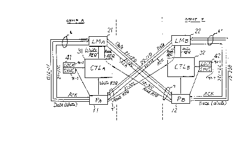
An embodiment of the present invention is hereinaf.~r
described referring to a principle block diagram of FIG. 5,
where the multiprocessor system is composed of t~.70
processors 11 (PA) and 12 (PB) shown as representatives of
a plurality of processors. Each processor PA and PB has
own local memory L~5A and LMs respectively. The term "own"
is used to mean "belonging to the same group", i.e. in
other words "accessible ~ithout using a network". The term
"other" is hereinafter used to mean the opposite of
"own". The memory LMA of the group A is accessed from
own processor PA and also from the processor Ps of the
other group B, thus the memory is shared by the two
processors. A control circuit 31 (CTLA) having a set
of flag bits 41, one named a LOCK bit another one named a SYNC
bit, are p~ovided in the group A, for controlling the
transfer of an access request from the processor PA or PB
to the memory LMA. Sy,mmetrically similar, to the control
circuit CTLA, a second control circuit 32 (CTLB? having a
set of flàg bits 42 is provided in the group B, for
controlling the ~rangfer of an access re~uest from the
processor PA or PB to the memory LMB. The function of the
control circuits and the flag bits shall be described in
detail later on.
Communication means 6 (or 6') bet~een the processors
PA (or PB) and each own local memory L~IA (or L~IB) are
-- 6 --
12918~7
composed of: data buses 11-2.1D, 12-22D, for each processor
PA, PB to write a data into each own memory L~A, LMB; and
access control lines 21-llC, 22-l~C, each for delivering an
acknowledge signal ACK to each request source PA, PB.
Communication means 7 (or 7') between the processor PA (or
PB) and the memories LMB (or LMA) of their respectively
opposite groups are composed of: data buses 21-12D, 22-llD,
for each processor PB, PA to read data out of their
respectively opposite group's memory LMA, LMB; access
control lines 21-12C, 22-llC, each for delivering an
acknowledge signal ACK to each request source PB, PA; and
access control lines 11-32C, 12-31C, each for delivering a
read request signal "Read REQ" from each other processor
PB, PA to each own control circuit CTLA, CTLB.
The functions of the flag bits ~1 (or 42) of the
processor PA (or PB) are as follows:
[l] The LOCK.bit 41-1 (or 42-1) and the SYNC bit 41-2
~or 42-2) of each group A, B are both set by
. initialization respectively by their own processor
PA (or PB).
12] The.LOCR bit 4i-1 (or 42-1) is set before the own
processor PA (or PB) writes data in the own memory
LMA (or LMB), as well as is reset after the writing
is finished, by the own processor PA (or PB).
[3] The SYNC bit is reset as soon as the own processor
~ PA (or PB) finishes writing data into the own memory
-- 7 --
.~ ~
129
LMA ~or ~Ms)
~41 When th~ ~OC~ bit and th~ SYNC bit ar~ both in a
SE~ st~te,
a read request ~ignal ~ead REQ~ from th~ oth~r
proces~or PB ~or PA) ~o th~ own me~ory LMA ~or ~MB)
1~ ~nhibitt~dt and
a wrlt~ r~qu~t slgnal ~Writ~ REQ~ from the own
proc~ssor PA ~or Ps) to tho own m0mory LMA ~or ~MB~
ls pQrD~itt~d.
151 Whon th- ~OC~ blt 1~ in a R~8ET stato and tho 5XNC
bit 18 ln a 8ET ~tate, th- ~Wrlt~ REQ~ from tho own
procQsJo~ PA, (or PB) is inhibitted and the ~'Read REQ"
from the other processors PB ~or PA) is permitted.
161 Wh-n th statu~ of th- flag blt~ ar~ other than
tho~- of aboY -d-~crib-d~ t~l and 1~1,
a writ- raqu-~t ~Wrlt- REQ~ from th- own proc~J~or
PA tor P~) to th- o~n m-mory ~MA ~or LMB) i~
lnhlbltt-d and
a r~ad r-qu-~t ignal ~Road RS~ from th- othor
proc~JJor P~ ~or PA) to tho o~n m~ory LMA ~or LMB)
18 p-r~ltt-d
Th- oporatlon of th- proc~-o~ ~ynchronization
according to th~ pr-~-nt inv~ntion i~ h~r~inaftQr
de~crib~d, r~f~rring ~o a ~ampl- ca3~ whor~ th- proc~s~or
PA wrltes data into tho own ~mory LMA and then tho other
procQ~or PB r~ad~ out thu3 written data, and th~ 3ame
- 8 -
~ J
lZ918Z7
sequence is repeated. A typical structure of the controlcircuit 31 or 32 (CTLA or CTLB) and the flag bits 41 (or
42) is shown in FIG. 6, and its truth table is shown in
FIG. 7, where a positive logic is employed. As shown in
FIG. 6, the control circuit CTLA 31 (or CTLB 32) is
composed of AND gates 3a, 3b, 3c and a delay circuit 3d.
The flag bit 41 is composed of widely used memory devices,
such as flip-flops, one, 41-1, for the LOCR bit and one,
41-2, for the SYNC bit. The AND gate 3a is gated by the
LOCR bit as well as the SYNC bit. One of the input
terminals of the AND gate 3c is gated by the read request
signal "Read REQ" from other processor 12 tPB), because the
data transfer is from the own processor 11 ~PA) to the
other processor 12 (PB). One of the input terminals of the
AND gate 3b is gated by the write request signal "Write
REQ" from the own processor 11 ~PA). The delay circuit 3d,
formed of widely used delay device to produce a
predetermined delay time, which is equivalent to the time
'required for finishing reading a data to be transferred by
a single operation. Accordingly, the SYNC bit 41-2 is
automatically set as soon as the reading is finished. Thus
the control circuit CTLA and the flag bits operate as shown
in the truth table of FIG. 7, where "y" indicates that the
request is permitted and "N" indicates that the request is
inhibitted.
Flows of the over all operations for synchronizing the
g _ ,
-
independently operating processors of the two groups, where
the A group includes the processors 11 (PA), the memory 21
(LMA), the circuit control and 31 (CTLA) and its flag bits
41, and the B group includes the processors 12 (Ps)~ the
memory 22 (LMB), the control circuit 32 (CTLB) and its flag
bits 42,is described below and shown in FIG. 8. The
numerals for the procedure steps are also cited in the flow
chart of FIG. 8. Dotted lines in FIG. 8 show "flows" of
the flag information.
(1) Each of the LOCR bits (41-1, 42-1) and SYNC bits
(41-2, 42-2) of the processors 11 and 12 is set as
an initialiæation before beginning the operation,
and in this state of the flag bits:
the own processor 11 (PA) is permitted to write into
the own memory 21 (LMA); and
the other processor 12 (PA) is inhibitted to read
the same memory 21 (LMA).
(2) The processor 11 (PA) be sure to set the LOCK bit
41-1 before writing data into the own memory 21
~LMA). (Bowever, the first setting after the
initialization is not necessary because the setting
is duplicate.)
(3) The processor 11 (PA) writes data into the own
memory 21 (LMA), and on the other hand, the other
processor PB has transmitted a read request signal,
Read REQ, to the control circuit 31 (CTLA) and been
-- 10 --
12918~7
waiting for the acknowledgement signal ACR.
(4) As soon as the writing-in is finished, the LOCK bit
41-1 as well as the SYNC bit 41-2 is reset, and
acknowledge signal ACK is transmitted from the
memory permitting the processor 12 (PB) to read out
the memory 21 (LMA).
(5) The control circuit 31 (CTLA) sets the own SYNC bit
41-2 at the predetermined delayed time after the
~Read REQ" signal from the other processor 12 (PB).
At this time the reading-out by the other processor
12 (PB) iS already finished.
(6) The processor 11 (PA) operates other jobs, which is
not related to the explanation of the invention, and
then;
returns to the step S2), and sets the own LOCK bit
41-1; and
writes into the own memory 21 (LMA) unless the SYNC
bit 41-2 is still in a RESET ~tate inhibitting the
writing.
(7) The processor 12 (PB) in the B group returns to the
step 4 after finishing other jobs.
Consequently, the above-described operation is
summarized as follows:
SA) When the processor PA is writing into the own memory
LMA, the other processor PB is inhibitted to read out this
memory LMA.
-- 11 --
12~918~7
(B) After the processor PA finishes writing into the own
memory LMA, this processor PA is inhibitted to write next
da~a into this memory until the other processor PB finishes
reading out this memory.
(C~ The processor PB i5 inhibitted to read out the other
memory LMA, after reading out the same memory until the
writing from the processor PA into the same memory is
finished.
Though in the above-described embodiment of the
invention the local memory LMA 1s written in exclusively by
the own processor PA as well as read out exclusively by
the processor PB of the other group B, it is apparently
pos~ible for the reverse case where the local memory LMB is
read out by the processor PA as well as written in by
the processor PB of its own group B.
Though in the above-described embodiment of the
invention a single set of flag bits having one for LOCR and
one or SYNC is provided in each group A or B, each group
may be provided with a plurality of the sets of flag bits,
wherein each set communicates with a corresponding one of a
plurality of the processors.
Though in the above-described embodiment of the
invention a set of the LOCK bit and the SYNC bit is
provided in association of with data of a single word, it
is also apparently possible to provide a set of LOCK and
SYNC bits associated with a set of data consist of a
- 12 -
:~ ."~Y
1291827
plurality of words, or to compose the local memory with aplurality of these sets.
The configuration of the control circuit 31 of FIG. 6
is referred to as a typical sample, any other circuit
configuration which achieves the above-described function
can be used in place of the circuit shown in FIG. 6.
Advantages of the present invention are:
Firstly the fact that the setting/resetting of the
flags can be carried out by the internal communication
within each group as well as by a memory access from other
group, contributes to achieve a simple network
configuration without requiring the control lines 4 used
only for synchronization.
Secondly the software can be perfectly free from the
job o synchronization, because the processor can be
del~ed by inhibitting the access request signal, resulting
in a reduced network traffic, that is, a high-speed
operation, and
Thirdly the simplified hardware helps achieve a
high-speed synchronization operation.
The many features and advantages of the invention are
apparent from the detailed specification and thus, it is
intended by the appended claims to cover all such features
and advantages of the system which fall within the true
spirit and scope of the invention. Further, since numerous
modifications and changes will readily occur to those
- 13 -
~2~318Z7
skilled in the art, it is not desired to limit the
invention to the exact construction and operation shown and
described, and accordingly, all suitable modifications and
equivalents may be resorted to, falling within the scope of
the invention.
- 14 -