Note : Les descriptions sont présentées dans la langue officielle dans laquelle elles ont été soumises.
~ 92~
BRUSHLESS MOTOR DRIVE CIRCUIT
BACKGROUND OF THE INVENTION
This invention relates to a drive circuit for
a brushless (BL) motor. More particularly, this
invention relates to a drive ~ircuit for a ~L motor
utilizing ~all elements to reduce acoustic noises
during phase switching. Still more particularly, this
invention relates to a drive circuit for a conventional
BL ~otor employing ~all elementQ for producing output
energization signals having a predetermined desirable
waveform for application to stator coils on the BL
~otor.
A number of swit~hing drive ~ystems for
~nerglzing conventional BL motors are known. Such a
witching drive system ~ometimes utilizes switching
transistors or switching the energiza~ion or phase for
such a conventional ~L ~otor. When using such a
switching drive system, a resulting high-frequency
mechanical vibration of stators and rotors of the BL
motor generates relatively loud acoustic noises which
are caused by abrupt current changes at the time of
phase switching. The acoustic noises are most
noticeable when caused by the changes occurring at the
rlsing edges o~ the applied motor current. Con-
ventionally, ~ondensers have been used ~o prevent thegeneration of the acoustic noises~ The condensers,
such as electro~ytic condensers, having a comparatively
large capacity, are ~onnected in parallel with the
~ stator ooils to 510w current changes during phase
30~ 8Witching.
The conventional method using such condensers
has disadvantages. ~ For example, the me~hod is not
effective ~when the ro~ation number of the motor is
small.~ Furthermore, use of condensers degrades motor
:.
.. . .
12.g~0~
- 2 -
efficiency because of the phase delay of an energi-
zation current which occurs wh;ch in ~urn causes an
invalid current to flow when $he rotation number of the
motor is large.
A linear drive system for a BL motor is also
known which utilizes a sinusoidal energization
current. While ~uch a circui~ is effective in reducing
acoustic noise, the motor drive efficiency is
remarkably lowered by such a linear drive ~ystem
compared with a 6witching drive system.
Accordingly, it has remained a problem in the
ar~ to redu~e a ~otor drive circui~ for a BL motor
which maintains ~otor effic;ency comparable with that
of a switching drive system, while reducing acoustic
noises dur ing ~hase switching.
Thus, it is an overall object of the invention,
therefore, to provide a BL motor drive circuit having a
motor efficiency which ~s comparable to the effictency
OE a switching drive system, while reduc~ng aCOUSttC
noi~es during phase switching.
It is another general object of this
invention to provide a BL motor drive circuit to
achieve those results by repla~ement of the drive
circuit, without altering the mechanical structure of
an conventional BL motor.
It is an additional object of this invention
to provide a BL motor drive circuit using output
: ~ignals of Rall elements for position detection to
produ~e waveforms having predetermined characteristics
to ~prevent acoustic noises during swi~ching while
: preserving the efficiency of the switching drive
system.
''i ~,,
p,~
~ 2 ~ 6
These and other objects and features of the
present invention will become apparent from the
foregoing detailed description of the invention and the
appended claims, with reference to the accompanying
drawings.
BRIEF SUMMARY OF T~E INVENTION
Directed to overcoming the problems noted
~bove with respect to the prior art and achieYing the
~bove~tated objects, the invention relates to a BL
~otor wi~h a three-phase bi-directional, 120
~nergization system, by way sf example. According to
the invention, outpu~ ~ignals ~rom a plurality of ~all
elements are provided for detecting ~he position of the
rotor and providing ~n enerqizat~on ~ignal through
accompanyin~ ~ircuitry having edge portions imilar to
inclined waveforms of the ~dge portion of the output
signals. The energization ~ignal~ are supplied to
stator ~oils o the BL motor, whereby acoustic noise
generation during switching ~s prevented with the same
efficiency as the swit~hing drive syste~.
The waveforms of ~he ~all elements depend
upon magnetic flux changes from rotor masnets in the BL
motor. ~hus, the waveforms of ~he output signals of
the ~all elements are almost trapezoidal, depending on
the distances between the rotor magnets and ~he ~all
elemen~s, the positions or ~izes of ~he non-magnetic
regions of the rotor magne~s, and o~her ~actors.
According to the invention, the edge portions of the
energization signals are formed by shifting the level
or a~plifying the edge p~r~ions at the output signals
of the Hall elements to provide the desired waveform
Accordingly, the çdge por~ions of the energization
signals do not become abrupt and thus prevent the
generation of acoustic noises. Because the output
waveforms are utilized according ~o the inven~ion, no
~2~
-- 4 --
phase change occurs even if the rotation number of the
BL motor varies. Moreo~er, since a trapezoidal drive
signal is thus employed, motor efficiency is not
lowered.
According to one aspect of the invention, a
BL motor drive circuit according to the invention
comprises a plurality of Hall elements for detecting
magnetic flux changes in a rotating rotor magnet.
drive signal generating circuit is connected to the
Hall elements for generating multi-phase drive signals
which are supplied to the stator windings of a multi-
phase BL motor. Each of the multi-phase drive signals
has a pair of slanted edge portions and a relatively
flat portion interposed between the pair of slanted
edge portions which are directly formed ~rom the
detected flux changes. Thus, the drive signal is
generally trapezoidal in shape. Preferably, the drive
signal generating circuit includes a signal clamping
circuit to form the flat portion of the generally
trapezoidal multi-phase drive signal, while a portion
of the slanted edge portions of adjacent pairs of the
multi-phase drive signals form an overlapping drive
area. The slanted edge portion of the multi-phase
drive signal subtends an electrical angle which lies
within the range of 2 el. to 30 el
In a typical operative embodiment, the drive
signal generating circuit includes a plurality of
buffer amplifying circuits connected to the Hall
elements; clamping circuits; non-adder mixing circuits;
analog switching circuits; and output amplifiers
respectively connected in series, a plurality of such
series circuits being respectivel~ connected in
parallel with the plurality of Hall elements. Each
drive signal generating circuit further includes
switching pulse generating circuits for generating
- s -
switching pulses supplied to the analog switching
circuits based upon detected magne-~ic flux changes. In
an alternative embodiment, non-adder mixing circuits
are replaced by signal mixing circuits in the series
arrangements. These and other features of the
invention will become apparent from a review of the
written description of the invention which follows,
~aken in conjunction with the accompanying drawings.
~RIEF DESCRIPTION OF THE DRAWINGS
In the drawings:
10Fig. 1 is a circuit diagram of a waveform-
shaping circuit for shaping the output signals of the
Hall elements, according to one embodiment of the
invention;
Figs. 2A and 2B are diagrams of waveforms at
selected points in the circuit of Fig. 1 for showing
the output waveforms from the respective Hall elements;
Fig. 3 is a circuit diagram of a circuit
according to the invention for developing the
energization signals from the output of Fig. 1.;
20Fig. 4 is a circuit diagram of a switching
pulse generator for providing switching signals
utilized in the circuit of Fig. 3;
Fig. 5 is a waveform diagram for describing
the operation of the switching pulse generating circuit
of Fig. 4;
Fig. 6, including Figs. 6A - 6H, is a
waveform diagram for ~se in describing the development
of the energization waveforms in the circuit of Fig. 3;
Fig. 7 is a circuit diagram of a portion of
another embodiment of the circuit, according to the
invention.
Fig. 8 is a circuit diagram of another
embodiment of a portion of the circuit according to the
invention.
12~9Z~
-- 6 --
Fig. 9, including Figs. 9A - ~E, is a
waveform diagram useEul in describing the development
of an energization waveform in an alternative
embodiment of t'ne invention; and
Fig. 10, including Figs. 10A - 10G, is
another waveform diagram for descc-ibing tne development
of the energization waveform in still another
embodiment of the invention.
DET~ILE~ DESCRIPTION OF THE PREFERRED EMBODIME~TS
A description of the embodiments of the
invention is provided according to the following
general sequence. First, the shaping of the waveform
of the output signals of the Hall elements is described
in connection with Figs. 1 and 2. Next, the circuit of
Fig. 3 for developing the energi~ation waveform is
described, followed by a description of the circuit for
generation of the switching pulses, referring to Fig.
4. Thereafter, the operation for developing the
energization waveform is described in connection with
Figs. 5 and 6, followed by a description of an
alternative embodiment in connection with Figs. 7 and
8. The waveform shaping of the output signals of the
Hall elements is further described in connection with
Figs. 9 and 10.
a. Waveform shaping of the output signals of thP Hall
elements.
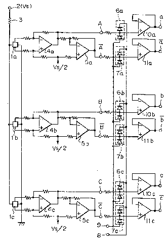
Fig. 1 shows a circuit for shaping the
waveform of the output signals from the Hall elements
utili~ed in the invention. A plurality of Hall
elements la, lb, and lc are provided for generating
output voltages proportional to the magnetic fluxes
from the rotor magnets of the BL motor. Each of the
Hall elements la, lb, and lc is driven by a drive
voltage obtained from an external C-ource of power Vs
provided to a power source terminal 2 through a
resistor 3 connected ~n common with an input of each of
the ~all elements. In the embodiment of Fig. 1, the
voltaqe Vs is maintained at a level equal to that
provided to the stator coils of the BL motor.
An output from each of the Hall element~ la,
lb, and lc is re~pectively amplified by pair~ of
operational amplifiers 4a, Sa; 4b, 5b; and 4c, 5c. In
the ampliiers 4a, 4~, and 4c, differential signals are
conver~ed into single-ended signal for inversion by
the inverting amplifiers 5a/ Sb, and Sc. Thus, a
detection signal A is obtained from the output of the
amplifi~r 4a, while a complementary detection signal
is provided at the ou~put of the amplifier 5a. The
detec~ion ~ignals A and ~ are opposite in phase.
Similarly, detec~ion signals B and C are
provided at the outputs from the amplifiers 4b and 4c,
respectively, while complementary detection signals ~
and ~, opposi~e in phase to the detection signals B and
~ respectively, are provided at the outputs of the
amplifieræ 5b and 5c.
Fig. 2A ~hows the phase relationship among
the respective detection signals A, B, and C provided
at the ou~puts of the amplifiers 4a, 4bt and 4c, as
shown in Fi~. 1. In Fig. 2A, the waveform shown in the
solid line represen~s the detection signal A, while the
waveform shown ~y the dotted~dashed line represents
the detection si~nal B. The waveform indicated by the
broken line represents the detection signal C. The
detection ~ignals A, B, and C produced by the circuit
of Fig. 1 are each generally trapezoidal in shape
havi~g a fla~ center portion and are superimposed about
an operating level of Vs~2. The respective detection
signals A, ~, and C differ in phase from aach other by
- 8 - ~6
120 electr~cally. The leading and trailing edges of
each of the detection waveforms A, B, and C are
inclined to prov$de a waveform which corresponds to the
sizes of the non-magnetic regions of the rotor magnets,
the gaps be~ween the rotor magnets and the ~all
elements, and other factors.
As hown in Fig. 1~ the detection signal A is
provided to a diode clamping circuit 6a, while its
complementary ~ignal ~ i8 provided ~o a diode clamping
circuit 7a. Similarly, the detection signals B, ~, C,
and ~ are respectively provided to diode clamping
circui~s 6b, 7b, 6c, and 7c. The diode clamping
circuits 6a, 6b, and 6c act ~o normalize the maximum
level of the detection .ignals A~ Br and C to a
clampiny Yoltage provided from a ~erminal 8 f~om an
external ~lamping voltage ssurce to each of th~ diode
clamping oircuits 6a, 6b, and 6c. The magnitude of the
clamping ~oltage applied to the terminal 8 is given by
~he expression 3Vs/4 - Vf, where Vf indicates a forward
voltage drop of the diode. The magnitude of the
voltage applied to the terminal 9 is given by the
expression Vs/4 + Vf. The terminal 9 ~s in circuit
with each of the diode clamping circui~s 7a, 7b, and
7cO
The output ~ignal from the diode clamping
circuit 6a is provided to an input of an operational
amplifier lOa acting as a buffer amplifier ~o provide
an output signal a. Similarly, the output signals from
the diode clamping circui~s 7a, 6b, 7b, ~c, and 7c are
respectively provided to an input of the operational
amplifiers llat lOb, llb, lOc, and llc, each of which
acts as a buffer amplifier similar to the buffer
amplifier lOa. The output signals from the buffer
amplifier~ lOa, lla, lOb, llb, lOc, and llc, are
respectively denoted by the letters a, a, b, 6, c, and
~- - 9 - ~z~
~, where, for example, the signal a is opposite in
phase to the ~ignal a. The signals a, b, and c are
shown ~n Fig. ~B.
The output siynals o~ Fig. 1, therefore, are
generally trapezoidal ~etection signals hav~ng a
maximum value of (3/4~ Vs, a mini~um value of (1/4) -
Vs, ~nd a center level of Vs/2, and the signal a is
~hown by the ~olld line ~n Fig. 2B. The outputs of the
operational amplifiers lOb and lOc, deno~ed by the
le~ters b and c are also generally ~rapezoidal ~n form,
~s seen in Fig. 2B, having maximum, minimu~, and
central levels ~imilar to the ~ignal a. Si~ilarly, the
complementary ~ignals a, S, and c which are opposite in
phase to the detection ignals a, b, a~d c, are
respectively output from the operational amplifiers
lla, llb, and llc, although not specifically ~hown in
Fig. 2B.
The above described detec~ion ~ignals, a, b,
c, and a, ~j and c, are used to develop the
energization waveforms for ~he ~tator coils on the BL
motor as will be b~tter understood from a discussion of
Figs. 3 and 6 later in this specification. The detec-
tion signals A, ~, B, ~, C, and ~ form switching
pulses, as discussed in connec~ion with Figs. 4 and 5.
b. Energiza~ion-waveform-developing circuit
~ ig. 3 ~hows a circuit for generating an
energization-waveform for ~he embodiment of Fig, 1.
3 The detection ~ignals a, b, and c and their
complementary detecti~n signals a, ~, and c, as
provided from Fig. 1 provide the inputs to the circuit
of Fig. 3. ~he output signals from ~he ~ircui~ of Fig.
3 are respectively provided to stator coils Ll, L2, and
L3 respectively. In the embodiment shown in Fig. 3, a
,~,
~ lo- ~2~2~
three-phase bi-directional energization circuit i~
shown in a structure in which an end of each of the
respective ~tator coils Ll, L2, and L3 ~s commonly
connected,, while the other end of each of the ~tator
coils is connected respectively ~o an output terminal
30a, 30b, and 30c of the circuit. Thus, ~he circuit
structure oE the 2nergiza~ion-waveform for the stator
coil Ll will be deccribed in detail, with the under-
~tanding that a similar circuit description of the
circuit ~tructure for the energization-waveform for the
5ta~0r coils L2 and ~3 is substant~ally identical and
ope~a~es in the same manner.
The detection 6ignal a from the Hall element
la and the detection signal ~, which ~s an invers~on of
the detection signal b from ~he Rall element lb, are
re~pectively provided to a non-adding mixing circuit
12a ~omprising a pair of diodes and a resistor,
connected as hown. A signal having a magnitude which
is the larger of the signals a and ~ is thus produced
from the non-adding mixing circuit l~a. The outpu~
~ignal of the non-adding mixing circuit 12a is provided
to an input of an operational amplifier 14a which acts
to buffer and cancel the diode forwar~ vol~age drop
(vf) .
The detection ~ignal a, which is the
inversion of the detection fiignal a, and the detection
signal b are respectively applied ~o an input of an
non-adding mixing circuit 13a, composed of diodes and a
resistor as shown and ~imilar ~o ~he mixing circuit
12a. A signal having a ~agnitude which ls ~he lesser
of the detection signals a and b is output from the
non-adding mixing circuit 13a. ~he output ~ignal from
the non-adding mixing ~ir~uit 13~ is provided to an
opera~ional amplifier 15a ~imilar ~o ~he ~mplifier 14a,
for buffering and cancelling the diode forward voltage
drop~
The output signals from the operational
ampliEiers 14a and 15a are respectively provided to an
inverting input of the operational amplifiers 16a and
17a. The operational amplifiers 16a and 17a act as
inversion amplifiers to shift the DC operating level.
The inverting terminal of the operational amplifier 16a
is connected through a resistance to a terminal 18 to
which is provided a direct current voltage having a
magnitude of Vs/4 which is added to the input signal of
the operational amplifier 16a. Similarly, a direct
current voltage of (3/4) Vs provided at a terminal 19
is added to the input signal of the operational
amplifier 17a. The non-inverting terminal of each of
the operational amplifiers 16a and 17a is connected to
a voltage having a magnitude of ~s/2.
The output terminals of the operational
amplifiers 16a and 17a are respectively connected to
analog switches 20a and 21a. The analog switches are
respectively controlled by switching signals on the
terminals 31 and 32, provided by the circuit of Fig. 4.
The output signal of the analog switch 20a is
provided to the analog switch 24a through an opera-
tional amplifier 22a acting as a buffer amplifier. The
output signal of the analog switch 24a is provided to
the base of an npn type transistor 26a which acts as an
output stage for the circuit. In a similar manner, the
output signal of the analog switch 21a is provided to
~ the base of a pnp type transistor 28a at the output
stage through an operational amplifier 23a and an
analog switch 25a. Each of the analog switches 20a and
24a turns on when a switching pulse from a terminal 31
achieves a high level. Similarly, each of the analog
switches 21a and 25a turns on when a switching pulse at
a terminal 32 assumes a high level. Thus, the analog
switches are respectively controlled in pairs by sig-
nals appearing at the terminals 31 and 32.
- 12 ~ 6
The emitter of ~he transistor 26a i5 coupled
to the base of an npn type ~ransistor 27a, while ~he
emitter of the transi~tor 28a is connected to a base of
an pnp type transi~tor 29a. The collector of the
~ransistor 27a is connected to a power source terminal
to which i8 provided a power ~ource voltage Vs, while
the ~ollec~or of the transistor 29a i~ connected to a
sourçe of reference potential, ~uch as ground. The
emitters of the transistors 27a and 29a are mutually
coupled to an output terminal 30a. A feedback loop is
provided from the output terminal ~o the inputs of the
opera~ional ampli~iers 22a ~nd 23a. Thus, an output
voltage, which does not ~ontain the base~emitter
voltage drops of the transistor~ ~nd is equal to the
input voltage of the operational amplifier~ 22a and
23a, is produced at the output terminal 30a.
Circu~t structures similar ~o that described
above for developing an output voltage generated at tbe
output terminal 30a are al80 provided in connection
with the output terminals 30b and 30c, respectively.
Specifically, a similar circuit is provided having as
~ts input the detection signals b, c, and ~, c, in
circui~ with output terminal 30b, and another circuit
having inputs c, a, and c, aO provides an output
at terminal 30c. Thus, an output voltage taken from
tXe output terminal 30b is for~e~ from the detection
signals b, c, ~, and c, at the outpu~ of the circuit of
Fig. 1, while an output ~oltage derived from the output
terminal 30c is formed from signals c, a, c, and a.
Thus, the componen~s shown in ~he remaining circuit of
Fig. 3 are similar in function and operation to those
de~çribed with respect ~o ~he ~ame reference numerals
above, but are appended with the letters b and c. It
~hould be no~ed ~hat a terminal 33 is provided as an
input terminal for a ~witching pulse for ~ontrolling
- 13 -~
the analog switches 20b and 24b, while an input
terminal 34 receives a switching pulse for controlling
the analog switches 21b and ~5b. Similarly, a
switching pulse is provided to a terminal 35 for
controlling the analog switches 20c and 24c, ~lhile a
switching pulse is provided at a terminal 36 for
controlling the analog switches 21c and 25c.
c Generation o~ switching pulses.
.
Fig. 4 shows a circuit for generating
switching pulses applied to the terminals 31-36 of Fig.
3 As shown in Fig. 4, a plurality of level
comparators 41-46 'nave their non-inverting terminals
commonly connected and have their inverting terminals
respectively connected to the non-inverting terminals
of a like plurality of level comparators 51-56. The
comparators 51-56 have their inverting terminals
commonly connected. A reference voltage having a
magnitude of (3/4)Vs is supplied to one of the input
terminals of each of the level comparators 41-46. The
level comparators 41-46 produce high level outputs when
the level of each input voltage given to the other
input terminal is lower than (3/4)Vs and, in the
opposite case, produce low level outputs. A reference
voltage having a magnitude of (l/4)Vs is applied to the
other input terminal of each of the level comparators
51-56, which generate high level outputs when the level
of each input voltage provided at one input terminal is
higher than (1/4)Vs and, in the opposite case, generate
low level outputs.
The detection signals A, B, and C from the
~all elements la, lb, and lc are supplied from the
circuit of Fig. 1 to the other input terminal of each
of the level comparators 41, 42, and 43 and one input
- 14 - ~
terminal of each of the level comparators 51, 52, and
53. Similarly, t'ne inverted detection signals ~
and ~ are provided to the other input terminal of each
of the level comparators 44, 45, and 46, and to one
input terminal of each of the level comparators 54, 55,
and 56. The outputs from the level comparator 51 and
the level comparator 55 are provided to an AND gate 61,
while the outputs ~rom the comparators 52 and 56 are
provided to an AND gate 63~ The outputs from the
comparators 53 and 54 and provided to an AND gate 65.
Similarly, the outputs from the level comparators 41
and 45 are connected to an AND gate 62; the outputs
from the level compara-tors 42 and 46 are provid~d to an
AN~ gate 64; and the outputs from the comparators 43
and 44 are provided to an AND gate 56. The AND gates
61, 63, and 65 respectively ~rovide outputs at
terminals 31, 33 and 35 which correspond to the
switching pulse terminals in Fig. 3. Similarly, the
AND gates 62, 64, and 66 provide output pulses at
terminals 32, 3~, and 36 which respectively provide
switching pulses to the corresponding input terminals
shown in Fig. 3. The operation of the circuit of Fig.
4 for generating switching pulses to the terminals 31
and 32 will be described, by way of example, by
reference to Fig. 5.
As shown in Fig. 5, on the basis of the
voltage level-relationship of the signal A, shown by a
solid line, and the signal ~, shown by a broken line,
with the reference voltages as previously indicated of
(~/4)Vs and (3/4)Vs, the output of the level comparator
41 assumes a high level when A is less than (3/4)Vs.
The output of the level comparator 45 assumes a high
level when ~ is less than (3/4)Vs. The output o the
level comparator 51 assumes a high level when the
magnitude of the detection signal A is greater than
~!92(~S
(1/4)Vs, while the output oE the level comparator 55
assumes a high level when ~ is greater than (l/4)Vs.
Consequently, the switching pulse produced by the A~ID
gate 61 at the terminal 31 and the switching pulse
Eormed by the AND gate 62 at the terminal 32 are those
shown by corresponding reference numerals in Fig. 5.
Thus, the analog switches 20a, 24a and the analog
switches 21a, 25a turn on during periods in which these
switching pulses have high levels, as previously
described.
A similar analysis applies to the relative
signal levels applied to the inputs of the AND gates 62
and 63 for generating switching pulses at the terminals
33, 34, 35, and 36.
d. Development of energization-waveforms.
Fig. 6, including Figs. 6A-H, provides a
diagram useful is considering the development of an
output voltage or an energization wave~orm generated at
the output terminal 30a at Fig. 3, using the switching
circuit of Fig. 4, by way of example. When the signals
a and ~ are provided to the non-adding mixing circuit
12a, a signal having a magnitude which is the larger oE
the magnitude of both signals, as shown in Fig. 6A, is
produced at the output of the operational amplifier
14a. Similarly, when the signals a and b are provided
to the non-adding mixing circuit 13a, a signal having a
magnitude which is the smaller of the level of both
signals~ as shown in Fig. 6B, is produced at the output
of the operational amplifier 15a. The output signal of
the operational amplifier 14a, as shown in Fig. 6A, is
the signal having a center level of (l/2)Vs, a maximum
value of (3/4~Vs, and a minimum value of (1/4)Vs, as
previously described. The output signal oF the
' - 16 ~ 3~6
operational amplifier 15a, as shown in ~ig. 6B, is a
signal having a similar series of levels. As ~hown in
Fig. 6C, a ~ignal having a level of [~1/2)Ys ~ Vs~ is
generated at the output of the amplifier 16a, as a
result of the rising shift of the (1/4~Ys level shown
in Fig. 6~ and its subsequent inversion. AB indicated
in ~ig. 6D, a signal having a level tO - (1/2~V~3 is
produced at the output of the operational amplifier 17a
~s a result of a decreasing shift of the (1/4)Vs level
of the signal shown in Fig. 6B and its inversion.
An almo~t high level period in the eignal
~hown in Fig. 6C is provided ~n ~he outpu~s of the
analog ~witches 20a and 24a by a ~witching pul~e from
the terminal 31, as shown in Fig. 6E. By a ~witching
pulse from the terminal 32, as ~hown in F;g. 6F, an
almost low level p~riod in the ~ignal hown in 6D is
provided a~ the outpu~s of the analog switches 21a and
25a. Therefore, an output voltage obtained by the
combination of the two signal waveforms gated by the
analog ~witches 21a and 25a is produced at the output
~erminal 30a, as shown in Fig. 6G.
Output voltages formed in a manner sim;lar to
the formation of the outpu~ voltage described above at
terminal 30a, are derived at the output terminals 3Qb
and 30c, respectively, using appropriately gated
voltage signals from the circuit of Fig. 4. As thus
~hown in Fiy. 6H, a waveform indlcated by a solid line
~hows an output voltage yenerated at ~he output
terminal 30a; a waveform indi~ated by a broken line
shows the output Yoltage generated at ~he output
terminal 30b; and the waveform indicated by a
dotted/dash line shows an output voltage appearing at
the output terminal 3Qc. As ~an b seen in Fig. SH,
the energization is sequentially accomplished for each
of ~he stator coils Ll, L2, and L3 for a slightly
larger energizing range than 120.
- 17 - ~ 6
Refer~ing again to Fig. 3, and assuming tnat
a current flowing through the stator coils ~l and L2 is
Il, and a current flowing throug'n the stator coils Ll
and L3 is I2, (where Il > I2), is established in the
interval in which the output terminal 30a has a voltage
signal hav ng a magnitude Vs, the output terminal 30b
thus has a magnitude (l/2)Vs, and the output terminal
30c has a zero voltage. Then, by a gradual decrease in
the magnitude of Il, accompanied by a gradual increase
in the magnitude of I2, the voltage at the output
terminal 30b and that at the output terminal 30c are
equal to (l/2)Vs to provide the relationship of (Il -
I2). With a further decrease of Il accompanied by a
further increase of I2, the condition wherein (Il < I2)
is established. In other words, phase switching is
performed gradually, and the generation of acoustic
noises due to an abrupt current change is prevented at
the time of the phase switchingO In addition, an
attenuation of the torque encounteeed with the phase
switching can be cancelled with overlapped energization
intervals at the time of phase switching at every 120
of an electrical cycle.
In Fig. 6H, even though the energization
waveforms cross at points 3/4 VS and 1/4 VS, the design
may be modified so that the crossing occurs at points
higher than 3/4 Vs and at points lower than 1/4 VS.
Furthermore, in the interval in which the energization
waveform assumes a cons-tant level of l/2 VS, no current
flows through one of the stator coils Ll, L2, and L3 to
achieve an im~rovement in motor efficiency as well as
to prevent generation of an uneven torque.
For t'ne above-described embodiment, the
detection signals a, b, and c having an amplitude oE
(l/2)Vs are formed with respect to the voltage Vs
applied to the stator coils Ll, L2 and L3. However,
- 18 -
the signals for the energi~ation may be provided by
amplifying detection signals having an amplitude of (~1
= Vs/2n) (where n is an integer! when the amplitudes of
the detection signals a, b, and c are represented by
~l. It may also be noted that an actual circuit is
constructed so that the inclination of the inclined
portions of the energization waveform are altered so as
to vary the hatched region shown in Fig. 6H within a
rarlge oE electrical angles from about 2 to 30.
e. Alternative embodiment
.
Figs. 7 and 8 show another embodiment of the
invention. This alternative embodiment develops the
energization waveform using signals a, ~, and ~, shown
in Fig. 9A, which are formed by mutually subtracting
two detection signals from the detection signals A, B,
and C, as shown in Fig. 2A, of the three Hall ele-
ments. Specifically, the signal a is formed by
subi:racl:ing detection signal A from detection signal B
(A - B); the signal ~ is formed from (B - C); and the
signal ~ is formed from (C - A). With this
energi~ation waveform using signals a, ~, and ~ , a
description of the development o-E an energization
waveform for one phase will now be provided.
Fig. 7 shows an example of an addition
circuit for developing the signal a . The addition
cLrcuit includes an operational amplifier 70 to which
ihe detection signal A and the detection signal B,
which is the inversion of the detection signal B, are
supplied as input signals. The signal a, which is
equal to (A ~ B = A - B) is consequently ~ormed with
the additlon circuit~ The signal a has a middle level
of (l/2)~s similar to the signals ~ and ~.
As shown in Fig. 8, the signal a is provided
at an input terminal 71 to t'ne inverting terminals of
an operational amplifier 72 and an operational
amplifier 73. The operational amplifier 72 produces a
signal ~ which is level-shifted by a voltage value of
(~V2/~ and inverted. The operational amplifier 73
generates a signal ~, which is level-shifted by a
value of (-V2/2) and invertedO In Fig. 9B, the
waveforms of the signals a.l and ~2, which thus dif~er
in magnitude by V2, are shown.
The signal ~2 is provided to an analog switch
74 and a level comparator 76. The signal ~ is
provided to an analog switch 75 and a level comparator
77. The level comparator 76 generates the switching
pulse as shown in 9C, which assumes a high level for a
period in which the level of t'ne signal a2 is larger
than the reference level of (l/2)Vs. On the other
hand, the level comparator 77 produces a switching
pulse, as shown in Fig. 9D, which assumes a high level
for a period in which the level of the signal ~l is
smaller than the reference level (l/2)Vs. Thus, the
analog switch 74 turns on during a period in which the
switching pulse from the level comparator 76 is
maintained at a high level. The waveform of the
signal a~ having a ~evel greater than (1/2)Vs in an
interval is provided to an output terminal 78. The
analoy switch 75 turns on during a period in which the
switching pulse from the level comparator 77 is held at
its high level, and the wave~orm o~ -the signal ~ 1,
whose level is smaller than (1/2)Vs in an interval, is
provided at an ou-tput terminal 79.
The stator coils are connected to the
respective output terminals 78 and 79 through output
circuits similarly to those used in the above-mentioned
embodiment. Output voltages generated at the output
- 20 ~ 6
terminals 78 and 79 by the output circuits are combined
to provide a voltage having a waveform as shown in Fig.
9E. The energization waveform shown in Fig. 9E is
~imilar o that ~hown in Fig. 6G. As a result, an
5 abrupt current change at th~ time of phase witching is
prevented and energizing levels are overlapped, while
interval6 in which no current flows through a stator
coil are formedO Thus, in this al~ernative
embod;mentr an inclined angle and an energization angle
of all energization waveform are ~et on the basis of a
offset amount, a reference vol~age for the level
~omparators9 and ~he l~ke, as previously described.
f. Modiication
.
The invention is applicable ~ot only ~o a ~L
motor of a three-phase bi-directional energiza~ion
~ystem, but also to a BL motor having a three-phase
120 and unidirectional energization system, a ~wo-
phase 90 energization system, and a four-phase 90
energization system.
Fig. 10 thus illus~rates in a waveform
diagram the development of energization waveforms in a
case in which the invention is applied to a BL motor of
a two-phase bi-directional, 90 energization systemO
Fig. lOA ~hows the detection signals A ~nd B of two
Hall elements. Assuming t~at the de~ection signals A
and B have an amplitu~e of vs~ ~or example, in a manner
similar to the above-mentioned original embodimen~, the
maxlmum values of both of the detection signals A and B
are detected to form a signal as shown in Fig. 10B.
The minimum values of both detection si~nals A and B
are detected to provi~e a si~nal as shown in Fig. lOC.
~ - 21 ~ 6
These switching pulses ~hown in Figs. 10D and
10E are generated from the detection signals A and B of
the Hall elements. Thus, the signal shown in Fig. 10B
is inverted and level-shifted, and the waveform of the
signal in a period i~ provided ~n which the switching
pul~e shown in Fig. 10~ $s maintained at high level.
By combining two waveforms ~ubjected to ~witching, an
energization waveform as Qhown in Fig. lOF is
obtained, Thus, as indicated ln Fi~. lOG, the
energlzation waveforms denoted a a solid line and a
broken line are provided to he stator coils. The
eneryization ~avefor~s thus shown in Fiys. lOF and lOG
have a 810w current ~hange at the time of the phase
switching and features similar to t~ose in the previous
~escribed e~bodiments.
Thus, a~cording to ~he invention, since a
current change is ~low at the time of phase switching,
generation of acoustic noises in a switching system is
prevented. Because the detection signals of the ~all
elements having inclined waveforms are used in this
invention as the inclined portions of the energi~ation
waveforms, no ~ondenser i8 needed, ~hus, resulting in a
low cost structure. In addition, even when the
rotation number of a motor is ~mall, such as at the
time of starting, acoustic noise is nevertheless
prevented. In addition, thP invention has an advantage
that the degrada~ion of ~otor efficiency as appears in
the linear drive ystem does no~ occur. Furthermore,
the invention can be provided in such a system by
~erely replacing the drive circuit, without altering
the mechanical structure of a brushless motor.
Thus, the present invention is not l;mited to
the oregoing embodiments, since manv l~o~lii~ations and
varia~ions ~re possible within the spirit and scope of
the appended claims of the inven~ion.