Note : Les descriptions sont présentées dans la langue officielle dans laquelle elles ont été soumises.
~ 53,703
BACKGROUND OF THE INVENTIO~
Field of the Invention
The subject matter of this invention is related
generally to electromagnetic contactors and more specifi-
cally to the magnetic armatures associated with suchelectromagnetic contactors.
Descri~tion of the Prior Art
Electromagnetic contactors are well known in the
art. A typical example may be found in U.S. Patent
3,339,161 issued August 29, 1967 to J. P. Conner et al.
entitled "Electromagnetic Contactor" and assigned to the
assignee of the present invention. Electromagnetic contac-
tors are switch devices which are especially useful in
motor-starting, lighting, switching and similar applica-
tions. A motor-starting contactor with an overload relay
system is called a motor controller. A contactor usually
has a magnetic circuit which includes a fixed magnet and a
movable maynet or armature with an air gap therebetween
when the contactor is opened. An electromagnetic coil is
controllable upon command to interact with a source of
voltage which may be interconnected with the main contacts
of the contactor for electromagnetically accelerating the
armature towards the fixed magnet, thus reducing the air
gap. Disposed on the armature is a set of bridging con-
tacts, the complements of which are fixedly disposed withinthe contactor case for being engaged thereby as the magnet-
ic circuit is energized and the armature is moved. The
load and voltage source therefor are usually interconnected
with the fixed contact~ and become interconnected with each
other as the bridging contacts make with the fixed
contacts.
Typically, contactors are classified as either DC
devices or AC devices. In alternating current contactors
magnetic noise is caused by the coil voltage returning to
zero at a rate determined by the frequency of the power
supply, typically this is 60 hertz. The nolse level is
reduced by addin~ shading coils to the magnetic circuit.
~ ~9Z~3 53,~03
The shading coil result in a current flow when the voltage
is zero. The current flow results in a force that keeps
the magnet closed and quiet. It is the movement of the
magnet due to the AC power that causes the noise. However,
in efficient low-cost, simple, electrical systems it would
be advantageous to eliminate the use of a shading coil. In
a ~C device magnetic noise is not considered a problem
because there are no zero voltage crossings. In both AC
and DC contactors a non-magnetic gap is often added to the
path of the magnetic system to limit the residual magnetism
that causes magnetic sticking. When an E-shaped magnet is
used in prior art systems an air gap is added to the
magnetic path of the center leg by making that leg shorter
than the outside legs. This air gap increases the magnetic
reluctance of the closed magnetic path thus reducing the
residual magnetism thus rendering the kickout spring more
effective for separating the magnets during a contactor
opening operation. However, in an E-shaped magnetic member
in an AC system vibration of the center lag due to the fact
that there is some room for movement thereof due to the
placement of the air gap therein causes deflection of the
spine of the E-shaped member allowing the outer pole pieces
to wipe against abutting complementary members of an
associated permanent magnet. The latter movement causes
the outer leg pole faces to wear which eventually causes
the center leg air gap to disappear and the residual
magnetism to increase dramatically. In the present system,
a periodic holding pulse is provided to the m~gnetic coil
even when the contactor is closed to maintain the contactor
in the closed state. This periodic signal causes vibration
of the center leg of the E-shaped magnetic member introduc-
ing noise due to the vibration of the center leg and the
rubbing of the pole pieces of the complementary outer legs
against each other. Yet it is still desirable to maintain
the air gap. It would be advantageous, therefore, if a
magnetic system could be discovered which had the benefits
of the central air gap to reduce residual magnetism and yet
3 3L;Z~Z~93
~ 53,703
which prevented vibration of the central leg to el.iminate
noise and wear.
~ ~v~Y ,. ~U~ '~ ENTION
In accordance with the invention, an electromag-
netic contactor is taught having an E-shaped magnetic
armature which is complementary to an E-shaped permanent
magnet. The central legs of both the E-shaped armature and
the E-shaped~permanent magnet have nipples or protrusions
disposed thereon which abut when the magnets are closed.
The nipples are formed in the surface of the magnet by
mill~ing away or otherwise removing portions on either side
thereof at the face region. In a preferred embodiment of
the invention 10 mils of magnetic face material is removed
on either side of the nipple on both the movable armature
and the permanent magnet. The abutting nipples or protru-
slons prevent longitudinal movement of the central leg of
the armature relative to the central leg of the permanent
magnet and yet still provide significant air-gap region to
reduce the effect of residual magnetism.
BRIEF DESCRIPTION OF THE DRAWINGS
For a better understanding of the invention,
reference may be had to the preferred embodiments thereof,
shown in the accompanying drawings in which:
Figure 1 shows an isometric view of an electro-
magnetic contactor embodying teachings of the present
invention;
Figure 2 shows a cutaway elevation of the contac-
tor of Fig. 1 at section II-II thereof;
Figure 3 shows force and armature velocity curves
for a prior art contactor with electromagnetic armature
accelerating coil, kickout spring and contact spring;
Figure 4 shows a set of curves similar to those
shown in Eig. 3 but for one embodiment of the present
invention;
Figure 5 shows a set of curves similar to those
shown in Fig. 3 and Fig. 4 but for another embodiment of
the invention;
~ 53,703
Figure 6 shows still another set of curves for
the apparatus of Figs. 4 and 5 for voltage and current
waveshapes;
Figures 7A throu~h 7D show a schematic circuit
diagram partiall.y in block diagram form for an electrical
control system for the contactor of Figs. 1 and 2;
Figure 8 shows a plan view of a printed circuit
board which includes the circuit elements of Fig. 7 as well
as the contactor coil, current transducers and voltage
transformers of Fig. 2;
Figure 9 shows an elevation o~f the circuit board
of Fig. 8;
Figure lO shows the circuit board of Figs. 8 and
9 in isometric view in a disposition for mounting in the
contactor of Fig. 2;
Figure 11 shows a circuit diagram and wiring
schematic partially in block diagram form for the contactor
of Figs. 2 and 7 as utilized in conjunction with a motor
controlled thereby;
Figure 12 shows a schematic arrangement of a
current-to-voltage transducer for utilization in an embodi-
ment of the present invention;
Figure 13 shows a schematic arrangement of the
transformer of Fig. 12 with an integrator circuit;
Figure 14 shows a plot of air gap length versus
the voltage-to-current ratio for the transducer arrange-
ments of Figs. 12 and 13;
Figure 15 shows an embodiment of a current-to-
voltage transducer utilizing a magnetic shim;
Figure 16 shows an embodiment of a current-to-
voltage transducer using an adjustable protrusion member;
Figure 17 shows an embodiment of a current-to-
voltage transducer utilizing a movable core portion;
Figure 18 shows an embodiment of a current-to-
voltaye transducer utilizing a powdered metal core;
Figure l9 shows an algorithm, READSWITCHES, in
block diagram form for utilization by a microprocessor for
.
s' ~LZ~
~ 53,703
reading switches and discharging capacitors for the input
circuitry of the coil control board of Figure 7;
Figure 20 shows an algorithm, READVOLTS, in block
diagram form for reading line voltage for the coil control
board of Figure 7;
Figure 21 shows an algorithm, CHOLD, in block
diagram form for reading the coil current for the coil
control circuit of Figure 7;
Figure 22 shows an algorithm, RANGE, in block
diagram form for reading line current as determined by the
overload relay board of Figure 7;
Figure 23 shows a schematic representation of an
A-to-D converter and storage locations associated with
determining line current as found in the microprocessor of
the coil control board of the present invention;
Figure 24 shows an algorithm, FIRE TRIAC, in
block diagram form for utilization by a microprocessor for
firing the coil controlling triac for the coil control
board of Figure 7;
20Figure 25A shows a plot of the derivatives of the
line current shown in Figure 25A;
Figure 25B shows a plot of a one-half per unit, a
one per unit and a two per unit sinusoidal representation
of a line current for the apparatus controlled by the
present invention;
Figure 25C shows a plot of resultant analog-to-
digital converter input voltage versus half~cycle sampling
intervals (time) or three examples of line current magni-
tude of Figure 25A;
30Fiyure 26 shows a representation of the binary
numbers stored in storage locations in the microprocessor
of Fig. 23 for Example l of an analog-to-diyital conversion
for six sampling times in the RANGE sampling routine of
Figure 22 for the one-half per unit line cycle;
35Figure 27 shows a representation of the binary
numbers stored in storage locations in the microprocessor
of Fig. 23 for Example 2 of an analog-to-digital conversion
~2~ 3
~ 53,703
for six sampling times in the RANGE sampling routine of
Figure 22 for the one per unit line cycle;
Figure 28 shows a representation of the binary
numbers stored in storage locations in the microprocessor
of Fig. 23 for E~ample~3 of an analog-to-digital conversion
for six sampling times in the RANGE sampling routine of
Figure 22 for the two per unit line cycle;
Figure 29 shows plots of VLINE, VRUN(T), and
VRUN(F) at the input of the microprocessor;
Figure 30 shows a plan view of a printed circuit
board similar to that shown in Figures 8 and 9 for utiliæa-
tion in another embodiment of the invention;
~ i~ure 31 shows a cutaway elevation of a contac-
tor similar to that shown in Figures 1 and 2 for another
embodiment of the invention; and
Figure 32 shows a sectional view of the contactor
of Fi~ure 31 along the section lines XXXII-XXXII.
DESCRIPTION OF THE PREFERRED EMBODIMENT
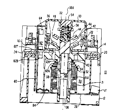
Referring to Fi~s. 1 and 2, a three phase elec-
trical contactor or controller 10 is shown. For thepurpose of simplicity of illustration the construction
features of only one of the three poles will be described
it being ~Inderstood that the other two poles are the same.
Contactor 10 comprises a housing 12 made of suitable
electrical insulating material such as glass/nylon composi-
tion upon which are disposed electrical load terminals 14
and 16 for interconnection with an electrical apparatus, a
circuik or a system to be serviced or controlled by the
contactor 10. Such a system is shown schematically in Fig.
11, for e~ample. Terminals 14 and 16 may each form part of
a set of three phase electrical terminals as mentioned
previously. Terminals 14 and 16 are spaced apart and
lnterconnected internally with conductors 20 and 24,
respectively, which extend into the central region of the
housing 12. There, conductors 20 and 24 are terminated by
appropriate fixed contacts 22 and 26, respectively.
Interconnection of contacts 22 and 26 will establish
.~
,~
~7 ~2~9~ 53,703
circuit continuity between terminals 14 and 16 and render
the contactor 10 effective for conducting electrical
current therethrough. A separately manufactured coil
control board 28 ~as shown hereinafter in Figs. 8, 9 and
10) may be securely disposed within housing 12 in a manner
to be described hereinafter. Disposed on the coil control
board 28 is a coil or solenoid assembly 30 which may
include an electrical coil or solenoid 31 disposed as part
thereof. Spaced away from the coil control board 28 and
forming one end of the coil assembly 30 is a spring seat 32
upon which is securely disposed one end of a kickout spring
34. The other end of the kickout spring 32 resides against
portion 12A of base 12 until movement of carrier 42 in a
manner to be described hereinafter causes bottom portion
42A thereof to pick up spring 34 and compress it against
seat 32. This occurs in a plane outside of the plane of
Fig. 2. Spring 34 encircles armature 40. It is picked up
by bottom portion 42A where they intersect. The dimension
of member 42 into the plane of Fig. 2 is larger than the
diameter of the spring 34. A fixed magnet or slug of
magnetizable material 36 is strategically disposed within a
channel 38 radially aligned with the solenoid or coil 31 of
the coil assembly 30. Axially displaced from the fixed
magnet 36 and disposed in the same channel 38 is a magnetic
armature or magnetic flux conductive member 40 which is
longitudinally (axially) movable in the channel 38 relative
to the fixed magnet 36. At the end of the armature 40 and
spaced away from the fixed magnet 36 is the longitudinally
extending electrically insulating contact carrier 42 upon
which is disposed an electrically conducting contact bridge
44. On one radial arm of contact bridge 44 is disposed a
contact 46, and on another radiaL arm of contact bridge 44
is disposed a contact 48. Of course, it is to be remem-
bered that the contacts are in triplicate for a 3 pole
35 contactor. Contact 46 abuts contact 22 (22-46), and
contact 48 abuts contact 26 (26-48) when a circuit is
internally completed between the terminal 14 and terminal
.. . .
~ ~3 53 703
16 as the contactor 10 closes. On the other hand, when the
contact 22 is spaced apart f~om the contact 46 and the
contact 26 is spaced apart from contact ~8, the internal
circuit between the terminals 14 and 16 is open. The open
circuit position is shown in Fig. 2. There is provided an
arc box 50 which is disposed to enclose the contact bridge
44 and the terminals 22, 26, 46 and 48, to thus provide a
partially enclosed volume in which electrical current
flowing internally between the terminals 14 and 16 may be
interrupted safely. Thare is provided centrally in the arc
box 50 a recess 52 into which the crossbar 54 of the
carrier 42 is disposed and constrained from moving trans-
versely (radially) as shown in Fig. 2, but is free to move
or slide longitudinally (axially) of the center line 38A of
the aforementioned channel 38. Contact bridge 44 is
maintained in carrier 42 with the help of a contact spring
56. The contact spring 56 compresses to allow continued
movement of the carrier 42 towards slug 36 even after the
contacts 22-46 and 26-48 have abutted or "made". Further
compression of contact spring 56 greatly increases the
pressure on the closed contacts 42-46 and 26-~8 to increase
the current-carrying capability of the internal circuit
between the terminals 14 and 16 and to provide an automatic
adjustment feature for allowing the contacts to attain an
abutted or "made" position even after significant contact
wear has occurred. The longitudinal region between the
magnet 36 and the movable armature 40 comprises an air gap
58 in which magnetic flux exists when the coil 31 is
electrically energized.
Externally accessible terminals on a terminal
block J1 may be disposed upon the coil control board 28 for
interconnection with the coil or solenoid 31, among other
things, by way of printed circuit paths or other conductors
on the control board 28. Another terminal block JX (shown
in Fig. 32) may also be disposed on printed circuit board
28 for other useful purposes. Electrical energization of
the coil or solenoid 31 by electrical power provided at the
~ 53,703
externally accessible terminals on terminal block J1 and in
response to a contact closing signal available at external-
ly accessible terminal block Jl for example, generates a
magnetic flux path through fixed magnet or slug 36, the air
gap 58 and the armature 40. As is well known, such a
condition causes the armature 40 to longitudinally move
within the channel 38 in an attempt to shorten or eliminate
the air gap 58 and to eventually abut magnet or slug 36.
This movement is in opposition to, or is resisted by, the
force of compression o the kickout spring 34 in initial
stages of movement and is further resisted by the force of
compression of the contact spring 56 after the contacts
22-46 and 26-48 have abutted at a later portion of the
movement stroke of the armature 40.
There may also be provided within the housing 12
of the contactor 10 an overload relay printed circuit board
or card 60 (also shown in Figs. 8, 9 and 10) upon which are
disposed current-to-voltage transducers or transformers 62
(only one of which 62B is shown in Fig. 2). In those
embodiments of the invention in which the overload relay
board 60 is utilized, the conductor 24 may extend through
the toroidal opening 62T of the current-to-voltage trans-
former or transducer 62B so that current flowing in the
conductor 24 is sensed by the current-to-voltage trans-
former or transducer 62B. The information thus sensed isutilized advantageously in a manner to be described herein-
after for providing useful circuit information for the
contactor 10.
There may be also provided at one end of the
overload relay board 60, selector switches 6~, which may be
accessible from a region external of th~ housing 12.
Another embodiment of the invention is depicted on Fig. 30
and Fig. 31 the description of which and operation of which
will be provided hereinafter.
Reerring now to Fig. 2 and Fig. 3, four superim-
posed curves are shown for the purpose of depicting the
state or the art prior to the present invention. In
,. .,~,
/ ~ 53,703
particular, plots of force versus distance for a magnetic
solenoid such as 31 in Fig. 2, a kickout spring such as 34
shown in Fig. 2, and a contact spring such as 56 shown in
Fig. 2, are depicted. In addition, a superi.mposed plot 92
of instantaneous velocity versus distance is depicted for
an armature such as 40 shown in Fig. 2. Although the
independent variable in each case is distance, it could
just as well be time as the two variables are closely
related for the curves shown in Fig. 3. It is to be
understood that the reference to component parts of the
contactor 10 of Fig. 2 is made for the purpose of simplify-
ing the illustration; it is not to be presumed that the
elements shown in Fig. 2, when taken together as a whole,
are covered by the prior art. There is shown a first curve
which depicts force versus distance (time could be
utilized) for a kickout spring (such as 34) as the spring
is compressed starting at point 72. The spring 34 offers
initial orce 74. The spring 34 gradually resists compres-
sion with greater and greater force until point 78 is
reached on the distance axis. The area enclosed by the
lines interconnecting point 72, point 74, the curve 70,
point 76, point 78 and point 72 once again represents the
total amount of energy that is necessary to compress a
kickout spring by the movement of the armature 40 as it is
accelerated to close the air gap 58 between it and the
fixed magnet 36. This force resists the movement of the
armature 40. At point 80 on the distance axis, the con-
tacts 22-42 and 26-48, for example of Fig. 2, abut, and
continued movement of the armature gO causes compression of
the contact spring 56 which operates to place increasing
force on the now abutted contacts for reasons described
previously. Curve 79 represents the total force which the
moving armature 40 works against as it is accelerated to
close the air gap 58. A step function increase in force
between point 81 and point 82 occurs as the contacts 22-42
and 26-48 touch. This force grows increasingly lar~er
until at point 78 the moving armature 40 experiences the
.~ ,
~ Z~3 53,703
maximum force applied by the combination of the kickout
spring 34 and contact spring 56. That amount of additional
energy which the moving armature must supply to overcome
the resistance of the contact spring 56 is represented by
the area enclosed by ~he lines which interconnect the
points 81 and 82, curve 7g, points 84 and 7~, curve 76A and
point 81 once again. Consequently, as the armature 40 is
accelerated from its position of rest at 72 to its position
of abutment against the magnet 36 at 78 the coil or sole-
noid 31 must supply at least the amount of energy repre-
sented by the lines which connect the points 72, 74, 81,
82, 84, 78 and 72 once again. The positive slope of curve
70 is purposely kept as small as possible consistent with
allowing the armature 40 to be driven in the reverse
direction when the coil energy is removed so that the
contactor may reopen. The initial force required to be
overcome by the armature 40 in its first instant of move-
ment is the threshold value of force represented by the
differenee between the points 72 and 74. Consequently, the
armature must supply at least that much force at that
instant of time. For purposes of simplicity of illustra-
tion, therefore, in an illustrative sense, it will be
presumed that the electromagnetic coil 31 provides the
force represented at point 88 in Fig. 3 for the armature 40
at 72. It is also necessary that the amount of force
provided by the coil or solenoid 31 at the instant that the
contacts 22-42 and 26-48 touch and the contact spring 56 is
engaged at 80 be greater than the amount of force repre-
sented by the distance between the points 80 and 82 in Fig.
3, otherwise, the accelerating armature 40 will stall in
midstroke, thus providing a very weak abutment of contacts
22-46 and 26-48. This is an undesirable situation as the
tendency for the contacts to weld shunt is greatly in-
creased under this condition. Consequently, the force
supplied by the coil 31 in acceleratiny the armature 40
must be greater at point 80 than the force represented at
point 82. A magnetic pull curve for solenoids and their
~. ,
~ 53,703
associated movable armatures follows relatively predictable
configurations which are a function of many things includ-
ing the weight of the armature, the strenyth o the magnet-
ic field, the size of the air gap, etc. Such a curve is
shown at 86 in Fig. 3. With the relative shape of the
curve 86 and the previous conditions of constraint associ-
ated with the value of the force required of the coil 31 at
points 72 and 80 on the distance axis of Fig. 3, the entire
profile for the magnet pull curve for the armature 40 and
coil 31 of Eig. 2 is fixed. It ends with a force value 90.
It is to be understood that it is a characteristic of
magnetic pull curves that the magnetic force increases
appreciably as the air gap 58 narrows as the moving arma-
ture 40 approaches the stationary magnet 36. Consequently,
at point 78, the force 90 exists. It is at this point that
the armature 40 first abuts or touches the fixed magnet 36.
This unfortunately creates two undesirable situations-
First, it can be easily seen that the total energy supplied
to the magnetic system by way of the coil 31, as repre-
sented by the lines which interconnect the points 72, 88,
curve 86, points 90, 78 and point 72 once again, is signif-
icantly greater than the amount of energy needed to over-
come the various spring resistances. The difference in
energy is represented by the area enclosed by the lines
which connect the points 74, 88, curve 86, points 90, 84,
82, 81 and 74 once again. This energy is wasted or unnec-
essary energy, and it would be very desirable not to have
to produce this energy. The second undesirable character-
istic or situation is the fact that the armature 80 is
accelerating at its maximum and producing its most force of
kinetic energy at the lnstant immediately before it makes
abutting contact with the permanent magnet 36. A velocity
curve 92 which starts ~t point 72 and ends at point 94 as
shown in Fiy. 3, represents the velocity of the armature 40
as it accelerates along its a~ial motion path. Note the
change in shape at 80 as the kickout spring 34 is engaged.
At the time immediately before the armature 40 touches the
~ .
~ 3 53,703
permanent magnet 36, the velocity Vl is maximum. Ihis has
the very undesirable characteristic of transferring high
kinetic energy due to high velocity at the instant of
impact or abutment between the armature 40 and the perma-
nent magnet 36. This energy must be instantaneouslydissipated or absorbed by other elements of the system.
Typically, the reduction of the armature velocity to zero
instantaneously at 78 requires the energy to be instantane-
ously reduced. This kinetic energy is converted to the
sound of abutment, to heat, to "bounce", to vibration, and
mechanical wear, among other things. If the armature 40
bounces, since it is loosely interconnected with the
contacts 46 48 on the contact bridge 44 by way of the
contact spring 56, there is a high likelihood that the
mechanical system represented thereby will oscillate or
vibrate in such a manner that the contact arrangements
22-42 and 26-4~ will rapidly and repeatedly ~ake and break.
This is a very undesirable characteristic in an electrical
circuit. It would thereore be desirable to utilize the
contactor 10 of Fig. 2 in such a manner that the energy
which is supplied to the coil 31 is carefully monitored and
chosen so that only the exact amount of energy (or an
energy value close to that amount) which is necessary to
overcome the resistance of the kickout spring 34 and the
contact spring 56 is provided. Furthermore, it would be
desirable if the velocity of the moving armature 40 is
significantly reduced as the armature abuts against the
permanent magnet 36 so that the likelihood of "bounce" is
correspondingly reduced. The solution to the aforemen-
tioned problems is accomplished by the present invention asshown graphically in Figs. 4, 5 and 6, for example.
Referring now to Fig. 2, Fig. 3 and Fig. 4, a
series of curves similar to those shown in Fig. 3 is
depicted in Fig. 4 for the present invention. In this
case, the spring force curves 70 and 79 for the kickout
spring 34 and contact spring 56 respectively are the same
as those shown in Fig. 3. However, the energy represented
~' '
- /~
~ 9Z~ 53,703
by the contact spring and kickout spring are designated X
and Y respectively. In this embodiment of the invention,
the magnet pull curve 86' representing the force applied by
the coil 31 startr, at point or force level 95 in order to
S overcome the kickout spring threshold force as described
previously and continues on to point or force level 97
which occurs at distance 96. It will be noted that the
electrical energy supplied to the armature 40 by the coil
31 ceases at distance 96 corresponding to force level 97.
This occurs before the armature 40 has completed its
movement to the position of abutment with fixed magnet 36.
It will be noted at this time that the maximum velocity Vm
attained by the armature 40 is indicated at point 98 on the
velocity curve 92'. This is the maximum velocity that the
armature will attain during its movement to the position of
abutment with the magnet 36. Said in another way, this
means that once the electrical energy has been removed from
the coil 31, the armature will cease accelerating and beyin
to decelerate. The deceleration curve is shown at 100 in
Fig. 4 and it ranges from point 98 to point 78 with a slope
change where the kickout spring is engaged. This is
accomplished by prematurely interrupting the flow of
electrical energy to the coil 31 at the time distance 96 is
achieved. Prior to the armature 40 completing its movement
to the position of abutment with fixed magnet 36, only that
amount of energy necessary to overcome the spring forces
need be applied, thus providing for an energy-efficient
system. At the time the electrical energy is removed from
the solenoid 31, the energy necessary to complete the
movement of the armature to its resting position of abut-
ment with magnet 26, is represented by the area enclosed by
the lines interconnecting the points 96, 99, curve 70,
points 81, 82, curve 79, points 84, 78 and 96 once again.
This energy is supplied during that portion of time that
electrical energy is being supplied to the armature coil 31
which is represented by the area Z (not necessarily to
scale) enclosed by the lines interconnecting the points 74,
" :~
~5~ 3
~ 53,703
95, curve 86', points 97, 99 and point 74 once again. The
latter-mentioned energy balance is chosen in some conve-
nient way which may include empirical analysis in which the
energy levels are determined experimentally. The energy
represented by area Z is utilized to compress the kickout
spring 34 during initial movement of the armature and is
not available for utilization later in the travel stroke.
As will be described hereinafter, a microprocessor may be
utilized to determine the amount of energy to be supplied.
The continued motion of the armature 40 during the deceler-
ation phase depicted by curve lO0 is a function of the
kinetic energy level E attained by the armature 40 at point
96 as the electrical energy is removed from coil 31. This
energy E is equal to one-half the mass (M) of the armature
times the velocity (Vm) it achieves at point 98 squared.
In a perfectly energy-balanced system, the decelerating
armature 40 strikes the permanent magnet 36 with zero
velocity at 78, thus eliminating bounce and the need to
absorb excessive energy in the form of noise, wear, heat,
etc. It is to be understood, of course, that the attain-
ment of the ideal as shown in Fig. 4 is difficult and is,
in fact, not necessary for a highly efficient system to be
nevertheless produced. Consequently, Fig. 4 should be
viewed as depicting an ideal system which is provided to
illustrate the teachings of the present invention. It may
become very difficult to have the armature 40 impact the
permanent magnet 36 with exactly zero velocity at 78. A
small residual velocity is tolerable, especially when
compared with the velocity 94 which is attained in the
prior system as shown in Fig. 3.
Referriny now to Fig. 2, Fig. 4 and Fig. 5, a
collection of curves similar to that shown in Fig. 4, is
depicted for a system in which the contact spring 56 is
stiffer and thus offers more force against which the moving
armature 40 must work. In addition to the foregoing, other
illustrative features are depicted; for example, the
electrical power is applied to the coil for a longer period
~C ~9~ 53,703
of time, thus allowing the velocity of the moving armature
40 to attain a higher value. The higher value of velocity
is necessary because increased kinetic energy is necessary
to overcome the increased spring force of the contact
spring 56. With regard to the comparison o Figs. 4 and 5,
like reference symbols represent like points on the curves
of the two figures. In the embodiment of the invention of
Fig. 5, the total energy necessary to compress the kickout
and contact springs 34 and 56, respectively, is increased
by an amount U represented by the area enclosed by the
curves or lines connecting the points 82, 102, curve 79',
points 104, 84, curve 79 and point 82 once again. The
remaining area, i.e., the area enclosed by the lines
interconnecting the points 72, 74, curve 70, points 81, 82,
15 curve 79, points 84, 78, and 72 once again, is the same as
that shown in Fig. 4. In order to provide the increased
energy U, a different magnet pull curve 86'' is generated.
This magnetic pull curve has a slightly higher average
slope and continues for a time period represented by the
20 distance difference between point 96 and point 100 thus
generating an incremental increase in energy U. The new
magnetic pull curve 86'' starts at point 95, which may the
same as that shown in Fig. 4, and ends at point 97' at time
represented by distance 100. This in turn generates a
steeper and longer velocity curve 92 " for the moving
armature 40. The peak velocity V2 is attained at point 98'
on velocity curve 92" . At this time, the kinetic energy
(E2) of the armature 40 i5 equal to one-half MV2 squared.
The instantianeous velocity then decreases, following curve
100' with a de~inite breakpoint at velocity Vl. This
breakpoint represents the armature initially abutting
against the contact spring 56. A portion of the increased
velocity V2 and thus increased energy E2 is quickly
absorbed by the previously described increase in energy
3S provided by the stiffened or more resistive contact spring
such that the curve 100' theoretically reaches zero at the
.
~ 53,703
point 78 which corresponds to the moving armature 40
abutting the fixed maynet 36.
Referring now to Figs. 2, 4 and 6, voltage and
current curves for the coil 31 and their relationship to
force curves of Fig. 4 are shown and described. In a
preferred embodiment of the invention, the coil current and
voltage are controlled in a manner described with respect
to the embodiment of Fig. 7 in a four-stage operation: (1)
the ACCELERATION stage, for accelerating the armature 40,
(2) the COAST stage, for adjusting the speed of the arma-
ture later in the armature movement operation prior to
abutment of the armature 40 with the fixed magnetic 36, (3)
the GRAB stage, for sealing of the armature 40 against the
fixed magnet 36 near or immediately after abutment to
dampen oscillation or bounce, if any, and (4) the HOLD
stage, for armature hold-in. Reference may be had to Table
1 to help understand the foregoing and that which follows.
Information from cable 1 is disposed as a menu in memory in
a microprocessor as will be described hereinafter. Elec-
trical energy is supplied to the coil or solenoid 31 at atime 72' which is related to point 72 on the distance axis
of Fig. 4 and ending at a time 96' which is related to
point 96 on the distance axis of Fig. 4 for the ACCELERA-
TION stage. The energy represented by areas Z and Z' in
Fig. 4 is provided by judicious choice of the electrical
voltage across the terminals of coil 31 and the electrical
current flowing therethrough.
~ 53, 703
~ o o ~ ~
w ~ . ~ ~ r o ~
~ . c~ __
z . _ z r ~ ~.
_ r
_ ~ ~ ~ n o
l _. ~ -- l ~ o-n D
l l ~ ~0,~
z ... . l
_
3 _ ~ _ oZ o
r~ ~ 8 lo
_ ~ :~ ¦ r
~ ~ ¦r
o~ ~ z ~)
. . ~ ~ c~
on
-~1 Aw l ;~ o- n o
. '~n o
.
o -~ 'o ~ o -~ cr ~ ~ ~D o n
o ?~ n ? ~ c~ D o
3 _ a l ~ o~7 =n ~ o
n ~ _ "-- n ~ t - l ~ ~~ n " ~
. _ ~ ,
~ D _ . _.
~3
_~ 53,703
The apparatus and method for controlling that voltage and
current will be described more ully hereinafter with
respect to Fig. 7. At this time, for purpose of simplicity
of illustration, the appropriate wave shapes will be shown
with the understanding that the apparatus for providing the
wave shapes will be described hereinafter. The voltage
available for being impressed across the terminals of coil
31 in a preferred embodiment of the invention may be
unfiltered full wave rectified AC voltage represented by
10 waveshape 106 with a peak magnitude 110. The electrical
current flowing through the coil 31 may be full wave
rectified, unfiltered conduction angle controlled AC
current pulses 108 which flow through coil 31 in accordance
with Table 1. Voltage may be impressed across coil 31 as
15 is shown at 106A, 106B, 106C, and 106D in Fig. 6. In one
embodiment of the invention, the total power supplied to
the magnetic coil 31 during the period between time 72' and
time 96' may be provided by adjusting the amplitude of a
full conduction current wave in conjunction with a known
20 peak amplitude 110 for the voltage wave 106 so that the
combination of the current and voltage which makes up the
power supplied to the coil 31 will be equal over the
aforementioned time period (72'-96') to the mechanical
energy required to close the contacts as described previ-
ously. In another embodiment of the invention, however, as
is indicated in Table 1, a gate controlled device such as a
triac may be connected in series with the coil 31 in a
manner to be described hereinafter with respect to Fig. 7
for rendering the coil generally non-conductive during
certain predetermined portions 1, a2, etc. of the half
wave current pulses 108 and thus for rendering the coil
generally conductive for the portions represented at ~1,
~2, etc. for the purpose of adjusting the total power
supplied to the coil 31 during the period of time (72'-96).
Note that between conduction intervals some coil current
flows due to the discharge of magnetically stored energy
which was built up during the preceding conduction
"
~,~
~3
~ 53,703
interval. In the preferred embodiment of the invention,
the number of conduction angle controlled pulses of current
108 is determined by the length of time that the magnetic
energy must be supplied by the coil 31 in the manner
described previously. In some embodiments of the inven-
tion, the appropriate adjustment to pulses 108 may be
accomplished before the time 96' and still accomplish the
appropriate supply of electrical energy to the coil 31 for
accelerating tha armature 40 in the manner described
previous. In another embodiment of the invention suffi-
cient energy may not be available from adjustment of the
current conduction cycle in the approprlate time and a
necessary later adjustment may be provided in a manner to
be described hereinafter. It is to be understood that the
smooth curves or waves 106 and 108, for example, are
illustrative of the ideal wave shapes envisioned but in
actuality may deviate therefrom. In the ideal situation
shown in Fig. 6, the armature 40 may be accelerated to a
level of ener~y E as shown in Fig. 4 at time 96' sufficient
to continue to compress the kickout spring 34 and contact
spring 56 with ever-decreasing armature velocity until a
point in time 78' is reached at which the armature 40
following curve 100 gently abuts against the magnet 36 with
zero velocity as is shown in Fig. 4. In actuality, howev-
er, the attainment of such is difficult. For instance, the
amount of electrical energy supplied by the combination of
the voltage waveshape 106 and the conduction-controlled
current waveshape 108 within the appropriate time t72'-96')
may be insufficient to supply the necessary kinetic energy
to the armature gO to allow it to complete the closing
cycle. This may be represented by velocity curve lOOA of
Fig. 4, for example, which shows the armature 40 stopping
or attaining a zero velocity, before it touches the fixed
magnet 36. In such a case the combination of the contact
spring ~6 and the kickout spring 34 would likely accelerate
the armature 40 back in the other direction until the
springs 34-56 had relaxed thus preventing closure of the
~ 3 53,703
electrical contacts mechanically interconnected with the
armature 40, thus, defeating the closing of the contactor
10. As undesirable as this situation may seem, a situation
in which the armature 40 almost touches the permanent
magnet 36 would be even worse as the likelihood of the
contacts stri~ing an arc therebetween and subsequent
contact welding is greatly increased. Recognizing that
insufficient energy may be available during the appropriate
time frame for accelerating the armature, a "mid-flight"
correction based on new information may be necessary to
"fine tune" the velocity curve of the armature 40. The
time for this correction occurs during the COAST part of
Fig. 6. Provision is made in the preferred embodiment of
the invçntion for re-accelerating the armature 40 by
providing an adjustment currerrt pulse 116 at a time 11~'
which deviates the deceleration curve of the armature from
curve 100 to curve 100B of Fig. 4 so that assured abutment
of the armature 40 with the permanent magnet 36 at rela-
tively low if not zero velocity may occur. This adjustment
pulse 116 is made by providing triac firing control angle
3 which may be greatly larger than angles al and a2, for
example. In a preferred embodiment of the invention, it is
envisioned that angles al and 2 are equal although this is
non-limiting and is merely a function of the control system
utilized for the current conduction path for the coil 31.
After the armature 40 has abutted the permanent magnet 36
at a relatively low velocity, the contactor 10 attains the
status of being "closed". Since it is possible that
vibration or other factors may induce contact bounce at
this time which bounce is highly undesirable, the control
circuit for the current in the coil 31 may be manipulated
in a convenient manner as described hereina~ter to provide
a number o "seal-in" or GRAB pulses for the abutting
armature 40 and fixed magnet 36. Since at least theoreti-
cally, the forward motion of the armature 40 has been, orwill shortly be, stopped by abutment with the magnet 36,
the introduction of seal-in pulses will not cause
~;
.~. ,. ~
2~
~ 53,703
acceleration of the armature because the armature's path is
p~ysically blocked by the disposition of the fixed magnet
36. Rather all oscillations will be quickly damped.
Assured seal-in of the contacts is thus attained. In a
preferred embodiment c,f the invention, seal-in or GRAB may
occur by allowiny coil current to flow for a portion of a
current half-wave represented by conduction angles ~4, 35
and ~6, for example, to generate seal-in or GRAB pulses
120. The ACCELERATION, COAST and GRAB operations work on
the principle of feed forward voltage control. In the last
stage of operation, HOLD, it is recognized that the mechan-
ical system has essentially come to rest but a certain
amount of magnetism is nevertheless necessary to keep the
armature 40 abutted against the fixed magnet 36 thus
keeping the contacts closed. A relatively small and
variable hold-in pulse 124 may be repeated once each
current half-cycle indefinitely for as long as the contacts
are to remain closed in order to prevent the kickout spring
34 from accelerating the armature 40 in the opposite
direction and thus opening the contacts. The amount of
electrical energy necessary to hold the armature 40 against
the magnet 36 in an abutted disposition is signiicantly
less than the amount necessary to accelerate the armature
~0 towards the magnet 36 to overcome the force of the
kickout spring 34 and the contact spring 56 during the
closing operation. ~he pulse 124 may be obtained by
significantly increasing the phase back, delay or firing
angle to a valuel a7 for example. Angle a7 may vary from
current pulse to current pulse, i.e., the next delay angle
a8 may be larger or smaller than angle a7. This may be
accomplished by closed loop current control; that is, the
current flowing in the coil 31 is sensed and readjusted if
necessary as is further described with respect to Fig. 21.
Referrlng now to Figs. 7A through 7D, an electri-
cal block diagram for the control circuit of the present
invention is shown. Coil control card 28 of Figs. 2, 8, 9
and 10 has provided thereon the terminal block or strip Jl
?i-
,y ~
s
23 ~Z~
for connection with external control elements such as shown
in Fig. 11 for example. Terminal block J1 has terminals 1
through 5 with designations "C", "E", "P", "3", and "R",
respectively. Connected to terminal "2" is one end of
S resistive element R1, Jne end of a resistive element R2,
and the first AC input terminal of a full-wave bridge
rectifier BRl. The other end of resistive element Rl is
connected to one end of a capacitive element C1, and one
end of a resistive element R16. This latter electrical
point is designated "120 VAC". The other end of the
resistive element R2 is the "LINE" input terminal of a
bipolar linear, custom, analog, integrated circuit module
Ul, the function of which will be described hereinafter.
This latter terminal is also connected to the B40 terminal
of a microprocessor U2 and to one side of a capacitance
element CX, the other side of which is grounded. Module Ul
is similar to apparatus described in U-S- pa~ent no. 4,626,831
entitled "Analog Signal Processing Circuit," and in U.S.
patent no. 4,674,035 entitled "A Supervisory Circuit for
a Programmed Processing Unit," both of which
are assigned to the assignee of this application. Micro-
processor U2 may be the kind manufactured by "Nippon
Electric Co." and identified as ~PD75CG33E or the kind
identified as ~PD7533. Connected to the second AC input
terminal of the bridge rectifier BR1 are one side of a
resistive element R6, the other side of which is system
grounded and the anode of a TRIAC or similar gated device
Q1. The other end of the capacitive element Cl is connect-
ed to the anode of a diode CR1, the cathode of a diode CR2
and the regulating terminal of a Zener diode ZNl. The
cathode of the diode CR1 is connected to one side of a
capacitive element C2, the other side of which is system
grounded, and to the "+V" terminal of the integrated
circuit U1. This latter point represents the power supply
voltage VY and in the preferred embodiment of the invention
is +lOVDC. The anode of the diode CR2 is connected to one
''':'1~
.~
~ ~2~ 53,703
side of a capacitive element C7, the other side of which is
grounded. The other terminal of the Zener diode ZNl is
connected to the non-regulating terminal of another Zener
diode ZN2. The other side or regulating terminal of the
Zener diode ZN2 is qrounded. The junction between the
anodes of the device CR2 and the capacitive element C7
carries the power s~lpply voltage VX which in a preferred
embodiment of the invention is designated -7V DC.
Input terminal "1" on terminal board Jl is
grounded. Input terminal "3" on terminal board Jl is
connected to one side of a resistive element R3, the other
side of which is connected to one side of a capacitive
element C4, to the "RUN" input terminal of the linear
integrated circuit Ul and to the B41 terminal of the
microprocessor U2. The other side of the capacitive
element C4 is grounded. Terminal "4" of terminal board Jl
is connected to one side of a resistlve element R4, the
other side of which is connected to one side of a capaci-
tive element C5, the "START" input terminal of the linear
circuit Ul and to the B42 terminal of the microprocessor
U2. The other side of the capacitive element C5 is con-
nected to ground. Input terminal "5" of the terminal board
Jl is connected to one side of a resistive element R5, the
other side of which is connected to one side of capacitive
element C6, the "RESET" input terminal of the linear
integrated circuit Ul and to the B43 terminal of the
microprocessor U2. The other side of the capacitive
element C6 is connected to ground. The combination of
resistive and capacitor elements R3-C4, R4-C5, and R5-C6
represent filter networks for the input terminals "3", "4"
and "5" of terminal board Jl, respectively These filters
in turn feed high impedance circuits represented by the
inputs "RUN", "START" and "RESET", respectively, of the
linear integrated circuit Ul.
Across the DC or output terminals of the full
wave bridge rectifier BRl is connected the aforementioned
solenoid coil 31 to be used in a manner previously
',~
~,
` ~2s~ ~z~
~ 53, 703
described and further described hereinafter. The other
main conduction terminal or cathode of the silicon-
controlled rectifier or similar gated device Ql is con-
nected to one side of a resistive e~ement R7 and to the
S "CCI" terminal of the device Ul. The other side of the
resistive element R7 is grounded. The gate o the silicon-
controlled rectifier or similar gated device Ql is con-
nected to the "C:ATE" output terminal of the linear inte-
grated circuit Ul.
The linear integrated circuit Ul has a "+5V"
power supply terminal which is designated VZ and which is
connected to the REF input terminal of the microprocessor
U2, and a resistive potentiometer element R8 for adjust-
ment. The integrated circuit module Ul has an output
terminal "VDD" which is connected to the VDD input terminal
of the microprocessor U2, to one side of a capacitive
element C16 and to one side of a resistive element R15, the
other side of which is connected to one side of a capaci-
tive element C9 and to the "VDDS" input terminal of the
linear analog module Ul. The other sides of the capacitive
elements C9 and C16 are grounded. The linear integrated
circuit module Ul also has a ground terminal "GND" which is
connected to the system common or ground. Integrated
cïrcuit Ul has a terminal "RS" which supplies the "RES"
signal to the RES lnput terminal of the microprocessor U2.
Linear integrated circuit module or chip Ul has a terminal
"DM" (DEADMAN) which is connected to one side of a capaci-
tive element C8 and to one side of a resistive element R14.
The other side of the resistive element R14 is connected to
the 022 terminal of the microprocessor U2. The other side
of the capacitor element C8 is connected to ground. Chip
or circuit Ul has a "TRIG" input terminal upon which the
signal "TRIG" is supplied from the B52 terminal of the
microprocessor U2. Integrated circuit Ul has a "VOK"
output terminal which provides the signal "VVDOK" to the
INTO terminal of the microprocessor U2. Finally, inte-
. ~i,,~
ill,9 ~, '/," '
~ ~ Z~ ~ 3 53,703
grated circuit Ul has a "CCO" output terminal whichprovides the signal "COILCUR" to the AN2 input terminal of
the microprocessor U2. Signal "COILCUR" carries an indica-
tion of the amoun-_ of coil current flowing in coil 31.
Further description of the internal operation of the
bipolar linear integrated circuit Ul and the operation of
the variously described inputs and outputs will be provided
hereinafter.
The other side of resistive element Rl6 is
connected to the anode of a diode CR4, the cathode of which
is connected to one side of a capacitive element Cl3, one
side of a resistive element Rl7 and the AN3 input terminal
of the microprocessor U2. The latter terminal receives the
signal "LVOLT" which is indicative of line voltage for the
system under control. The other side of the capacitive
element Cl3 and the other side of the resistive element Rl7
are system grounded.
There is also provided on the coil control board
28 another connector or terminal block J2 having terminals
upon which the following signals or functions are provided
"GND" (connected to ground), "MCUR" (an input), "DELAY" (an
input), "~5V" (power supply), "+lOV" (power supply) and
"-7V" (power supply). The control signals Z, A, B, C and
SW are also provided here.
The following terminals of the microprocessor U2
are grounded: GND and AGND. The terminal AN2 of the
microprocessor U2 is connected to the "MCUR" terminal of
the terminal board J2. Terminal CL2 of microprocessor U2
is connected to one side of a crystal Yl, the other side of
which is connected to terminal CLl of the microprocessor
U2. Terminal CL2 is also connected to one side of the
capacitive element Cl4. Terminal CLl is also connected to
one side of capacitive element Cl5. The other sides of the
capacitive elements Cl4 and Cl5 are connected to system
ground. Terminal DVL of microprocessor U2 is connected to
the "~5V" terminal on terminal board J2.
.,:r~
~1 ~2~Z~ 53,703
The linear analog circuit Ul internally includes
a regulated power supply RPS, the input of which is
connected to the "+V" input terminal and the output of
which is connected to the "+5V" output terminal. In a
preferred embodiment ~f the invention, the unregulated 10
volt value VY is converted within the regulated power
supply RPS to the highly regulated 5 volt signal VZ or +5V.
In addition, an internal output line COMPO for the regulat-
ed power supply RPS which in a preferred embodiment of the
invention may be 3.2 volts is supplied to the reference
terminal (-) of a comparator COMP. One input (~) of the
comparator COMP is provided with the VDDS signal. The
output of the comparator COMP is is designated VOK. The
input terminals designated "LINE", "RUN", "START" and
"RESET" are connected to a clipping and clamping circuit
CLA in the linear integrated circuit Ul which in a pre-
ferred embodiment of the invention limits the range of the
signal supplied to the microprocessor U2 to between ~4.6
volts positive and -.4 volts negative regardless of whether
the associated signal is a DC voltage or an alternating
voltage signal. Internal of the linear circuit Ul is a
gate amplifier circuit GA which receives its input from the
"TRIG" input and supplies the GATE output. Eurthermore, a
DEADMAN and reset circuit DMC which is interconnected to
receive the DEADMAN signal "DM" and to provide the reset
signal RES at l'RSII also provides an inhibit signal for gate
amplifier GA at III'I such that the gate amplifier GA will
produce no gating signal GATE if the DEADMAN function is
occurring. There is also provided a coil current amplifier
CCA which receives the coil current signal from terminal
"CCI" and provides the output signal COILCUR at terminal
CCO for utilization by the microprocessor U2 in a manner to
be described hereinafter. The description of the functions
provided by the microprocessor U2 at the various input and
output terminals thereof will be described hereinafter.
There is also provided the overload relay board
, .
~ 3 53,703
60 which includes a connector J101 and connector J102 which
are complementary with and connectable to the connector J2
on coil current control board 28 by way of a cable 64. The
previously-mentioned current-to-voltage transducer former
62 may be represented by three transform~ers 62A, 62B and
62C, respectively for a three-phase electrical system which
is controlled by the overload relay board 60. One side of
each of the secondary windings of these current-to-voltage
transducers 62A, 62B and 62C is grounded while the other
side is connected to one side of a resistive element R101,
R102 and R103, respectively. There is also provided a
triple two-channel analog multiplexer/demultiplexer or
transmission gate U101 having terminals aOR, bOR and cOR
connected to the other sides of resistive elements R101,
lS R102 and R103, respectively. The ay, by and cy terminals
of gate U101 are connected to ground. Terminals ax, bx and
cx of gate U101 are all tied together electrically and
connected to one side of an integrating capacitor C101 and
the anode of a rectifier CR101. The other side of the
capacitor C101 is connected to the cathode of a rectifier
CR102, the anode of which is connected to the cathode of
the aforementioned rectifier CR101, to the output of a
differential amplifier U103 and to the bOR terminal of a
second triple two-channel analog multiplexer/demultiplexer
25 U102. The other side of the integrating capacitor C101 is
also connected to the positive input terminal of a buffer
amplifier with gain U105 and to the cOR output terminal of
the aforementioned second analog multiplexer/demultiplexer
or transmission gate U102. The aforementioned joined
terminals ax, bx and cx of transmission gate U101 are also
connected to the ay and cx terminals of the transmis3ion
gate U102. The ax terminal of the transmission gate or
analog multiplexer/demultiplexer U102 is connected to
ground. The aOR terminal of the device U102 is connected
to one side of a capacitive element C102, the other side of
which is connected to the bx terminal of the multiplexer/
demultiplexer U102 and to the negative input terminal of
12~2~3
~q
~ 53,703
the aforementioned differential amplifier Ul03. The
positive input terminal of the aforementioned differen-
tial amplifier U103 is grounded. The negative input
terminal of the differential amplifier U105 is connected to
the wiper of a potentiometer P101, one main terminal of
which is grounded and the other main terminal of which is
connected to provide the "MCUR" output signal to the
terminal board J102. This latter signal is provided from
one side of a resistive element Rl03, the other side of
which is connected to the output of the differential
amplifier Ul05, the anode of a diode CR104 and the cathode
of a diode CR105. The anode of the diode CR105 is connect-
ed to ground and the cathode of the diode CR104 is connect-
ed to the +5V power supply terminal VZ. Devices U101, U102
and U103 are supplied from the -7 power supply. The +lOV
power supply voltage is supplied to the aforementioned
amplifier-with-gain U105 and to one side of a resistive
element 104, the other side of which is connected to supply
power to the aforementioned transmission gates U101 and
U102 as well as the anode of a diode CR106, the cathode of
which is connected to the +5V power supply voltage. The
+5V power supply level VZ on terminal board J102 is also
supplied to one side of filter capacitive element C103, the
other side of which is grounded and to one main terminal of
a potentiometer P102, the other main terminal of which is
grounded. The wiper of the potentiometer P102 is connected
to provide the 'IDELAYI' output signal on terminal board J101
and thence to terminal ANO of microprocessor U2. The
control terminals A, B and C of the aforementioned analog
multiplexer/demultiplexer device U101 are connected to the
A, B and C signal terminals, respectively, o~ a parallel to
serial eight-bit static shift register U104. Signals A, B
and C come from terminals 032, 031 and 030, respectively,
of microprocessor 42.
There is provided an eight-pole switch SWlOl with
the following designations: AM, CO, Cl, SP, HO, Hl, H2, and
H3. One end of each of the switch poles is grounded while
3 ~ 3
~ 53,703
the other end of each is connected to the 5 volt power
supply VZ by way of the PO through P7 input terminals of
the parallel to serial eight-bit static shift register
U104, the "COM" o~tput terminal of which receives the "SW"
signal from terminal koard J101 and the terminal I10 of
microprocessor U2. The previously described designations
"HO" through "H3" represent "heater" classes for the types
of devices controlled by the overload relay board 60.
Proper manipulation of any or all of the latter four poles
in switch SW101 provides a convenient way to represent the
heater class of the device protected by the overload relay
board 60.
Referring now to Figs. 2, 8, 9 and 10, construc-
tion features of the printed circuit board which is uti-
lized to make the coil control board 28 and the overloadrelay board 60 are illustrated and described. In particu-
lar, the terminal block J1 is shown disposed upon the coil
control board 28. Also shown disposed upon the coil
control board 28 is the coil assembly 30 (without coil).
The coil control assembly 30 includes the spring seat
arrangement 32 and a coil seat arrangement 3lA. There is
also disposed on the coil control board 28 the connector J2
into which is soldered or otherwise disposed one end of the
flat ribbon cable 64. Flat ribbon cable 64 is terminated
at the other end there of at the connectors J101 and J102
on the overload relay board assembly 60. The three-phase
current transducers or transformers 62, depicted as 62A,
62B, 62C in Fig. 8 for three~phase electrical current, are
shown on the overload relay board 60. There is provided
the switch SW101 which is an 8-pole dip switch. Also shown
are the potentiometers P101 and P102 for factory calibra-
tion and time delay adjustment, respectively.
In a preferred embodiment of the invention, the
coil control board 28 and the overload relay board 60 may
be formed on one piece of preshaped, soldered and connected
printed circuit board material. The single piece of
printed circuit board material is then separated at region
~, ~
3l ~Z ~ 2 ~g ~ 53,703
100 by breaking the isthmus 102, for example, to form a
hinged right angle relationship between the overload relay
board 60 and the coil control board 28, depicted best in -~
Figs. 2 and 10.
Referring now to Fig. 2 and Fig. 11, an illustra-
tion and exemplary but non-limiting control arrangement
utilizing the apparatus and electrical elements of the coil
control board 28 and the overload relay board 60 is shown.
In particular, there are provided three main power
lines--Ll, L2, L3--which provide three-phase AC electrical
power from a suitable three phase power source. These
lines are fed through contactors MA, MB, MC respectively.
The terminal board Jl is shown with its terminals designat-
ed: "C", "E", "P", "3" and "R". These designations repre-
sent the functions or connections: "COMMON", "AC POWER",
"RUN PERMIT/STOP", "START-REQUEST", and "RESET", respec-
tively. As was shown with respect to Figs. 8, 9, 10 for
example, the coil control board 28 communicates with the
overload relay board 60 by way of the multipurpose cable
64. The overload relay board 60 has, among other things,
the switch SW101 thereon which performs the functions
described previously. In addition, the secondary windings
of the current transducers or transformers 62A through 62C
are shown interconnected with the overload relay board 60.
The transducers 62A through 62C monitor the instantaneous
line currents iLl, iL2 and iL3 in lines Ll, L2, L3, respec-
tively, which are drawn by a MOTOR interconnected with the
lines Ll, L2, L3 by way of terminals Tl, T2, T3, respec-
tively. Power i9 provided to the coil control board 28 and
the overload relay board 60 by way of a transformer CPT,
the primary winding of which is connected across lines Ll,
L2, for example. The secondary winding thereof is connect-
ed to the ~C~ and "E" terminals of the terminal board Jl.
One side o the secondary winding of the transformer CPT
may be interconnected to one side of a normally closed STOP
pushbutton and one side of a normally open RESET pushbut-
ton. The other side of the STOP pushbutton is connected to
2~L~3
~ 53,703
the "P" input terminal of the Jl terminal board and to one
side of a normally opened START pushbutton. The other side
of the normally open START pushbutton is connected to the
"3" input terminal of the terminal board Jl, The other side
of the RESET pushbutton is connected to the reset terminal
R of the terminal board J1. The aforementioned pushbuttons
may be manipulated in a manner well known in the art to
provide control information to the coil control board 28
and overload relay board 60.
Referring now to Figs. 2, 7C and 12 through 18,
the construction and operation features of various kinds of
current transformers or transducers 62 associated with the
present invention are described. Conventional prior art
current sensing transformers produce a secondary winding
current which is proportional to the primary winding
current. When an output current signal from this type of
transformer is fed to a resistive current shunt and voltage
across the shunt is provided to a voltage-sensing electron-
ic circuit such as might be found in the overload relay
board 60, a linear relationship between input and output
exists. This voltage source then can be utilized for
measurement purposes. On the other hand, air-core type
transformer, sometimes called liner couplers, may be used
for current-sensing applications by providing a voltage
across the secondary winding which is proportional to the
derivative of the~ current in the primary winding. The
conventional iron-core current transformer and the linear
coupler have certain disadvantages. One is that the
"turns-ratio" of the conventional transformer must be
varied to change the output voltage for a given current
transformer design. In the current transformers or trans-
ducers described with respect to the present invention, the
rate of change with respect to time of the magnetic flux in
the magnetic core of the transducer is proportional to the
current in the primary winding absent flux saturation in
the core. An output voltage is produced which is propor-
tional to the derivative of the current in the primary
,,.~
3~ 3
3~ 53,703
winding, and the ratio of the output voltage to current is
easily changed for various current-sensing applications.
Iron core transformers tend to be relatively large. The
transformer of the present invention may be miniaturized.
Referring specifically to Fig. 12, a transformer
62X of the present invention may comprise a toroidal
magnetic iron core 110 with a substantial discrete air gap
111. The primary current iLl, i.e., the current to be
sensed, passes through the center of the core 110 and hence
provides a single turn input primary winding for the line
L1. The secondary winding 112 of the transformer 62X
comprises multiple turns which may, for the purposes of
illustration, be designated as having N2 turns. The
secondary winding 112 has sufficient turns to provide a
voltage level which is sufficient to drive electronic
circuitry which monitors the transformer or transducer.
The circumferential length of the iron core 110 is arbi-
trarily chosen for purposes of illustration as l1 and the
length of the air gap 111 is arbitrarily chosen as 12. The
cross-sectional area of the core is designated A1 and the
cross-sectional area of the air gap is designated A2. The
output voltage of the transformer is varied by changing the
effective length of the air gap 12. This can be
accomplished by either inserting metallic shims into the
25 air gap 111 as is shown in Figs. 15 and 16, or by moving
separate portions of the core structure of the transformer
as shown in Fig. 17, to provide a relatively smaller or
larger air gap 111. Once the length of the air gap 111 has
been chosen, a relatively small current-sensing transformer
or transducer is formed which produces an output voltage
eO(t~ which is generally proportional to the derivative of
the input current iLl in the input winding of the trans-
former. One advantaye o this arrangement is that it is
not limited to use on sinusoidal or even periodic input
currents. However for purposes of simplicity of illustra-
tion the following will be described with a sinusoidal
input current. The output voltage eO(t) produced by the
33
,~ ~
~ 53,703
secondary winding of the transformer or transducer 62X
shown in Eig. 12, for example, is given by Equation
( 1 ) :
eO(t) = ~ dt (ILl Sin ~t) (1)
~lAl ~2 A2
The terms ~1 and ~2 are the magnetic permeabi~ity of the
core 110 and air gap 111, respectively. ~ (omega) is the
frequency of the instantaneous current iLl and ILl equals
the peak magnitude of the instantaneous current iLl. For
applications where all parameters remain constant except
the length of the air gap 12 and the applied frequency ~,
equation (1) reduces to equation (2):
o(t) kl ~ k2Q2 [~ILl Cos ~t] ~2)
where the bracketed term is equivalent to the derivative
portion of Equation (1).
If the voltage eO(t) of equation (2) is supplied
to the terminals of an integrating circuit or integrator
such as 113 shown in Fig. 13 which, in a preerred embodi-
ment of the invention, may be as shown in Fig. 7, equation
(3) applies at the output of the integrator 113.
kl k2Q2 ILl Sin ~t (3)
As the length l2 of the air gap 111 is varied, the output
voltage e'0(t) which is now directly proportional to the
input current iLl will vary in inverse proportion to the
. I
3~ 3
~ 53,703
of the output voltage e'0(t) divided by the input current
(iLl for example) for variations in the length 111 of the
air gap 12. In a special case where the primary frequency
length 12 of the air gap 111. Fig. 14 shows a typical plot
~ remains constant or is assumed to be constant, the use of
the integrating circuit or integrator 113 of Fig. 13 may be
eliminated. In this case, equation (2~ can then be depict-
ed as shown in e~uation (4).
eO(t) = k + k212 ILl Cos ~t
where the constant frequency term ~ forms part of k4. In
this case the output eO(t) from the transformer secondary
winding 112 is proportional to the input current ILl and
varies inversely with the length 12 f the air gap 111.
Referring specifically to Figs. 15, 16, 17, in
applications where it is desirable to use the same current
transformer or transducer for sensing several ranges of
current, the output voltage eO(t) may be varied by
effectively changing the length 12 f the air gap 111.
This is accomplished by inserting a shim in the air gap of
the transformer 62Y of predetermined width, depending upon
the range of output voltage eO(t) desired. Alternately, a
wedge-shaped semicore 119 may be inserted into the air gap
111 o~ the transformer 62Z for accomplishing the same
purpose; and finally, the core of the transformer may be
25 cut into two sections--116A, 116B--for the transformer 62U
of Fig. 17 to accomplish the same purpose, by providing two
complementary air gaps 111~, lllB. Figures 12-17 teach a
current-to-volta~e transformer which has a primary winding
disposed on a magnetic core for providing magnetic flux in
the magnetic core in general proportion to the amount of
electrical current flowing in the primary winding. The
magnetic core has a discrete but variable air gap. The
discrete but variable air gap has a first magnetic reluc-
3 ~2~ 53,7~3
tance which prevents magnetic saturation of the magnetic
core for values of electrical current which are less than
or equal to a value Il. There is also provided a secondary
winding which is disposed on the magnetic core for
producing an electrical voltage V at the output terminals
theraof which is generally proportional to the magnetic
flux in the magnetic core. Voltage V is less than or equal
to voltage V2 for the first magnetic reluctance and for
values of current I less than or equal to Il. The variable
but discrete air gap is changeable to provide a second and
higher value of air gap reluctance which prevents magnetic
saturation of the magnetic core for values of electrical
current I less than or equal to I2 where I2 is greater than
Il. The voltage V remains less than or equal to Vl for the
second value of air gap reluctance and for values of
current less than or equal to I2.
Referring specifically to Fig. 1~, a homogeneous
magnetic core 120 for a transformer 62S may be provided
which apparently has no large discrete air gap 111, but
which, in fact, is comprised of sintered or compressed
powdered metal in which microscopic clumps or quantrums of
magnetically conductive core material 122 with homogeneous-
ly or evenly distributed air gaps 124. This has the same
effect as a discrete air gap such as 111 shown in Fig. 12
but reduces the effect of stray magnetic field influences
and provides a very reliable and small transformer. This
type of transformer may be formed by compressing powdered
metal or otherwise forming it into a core shape which has
sections of powdered metal 122 and the air gaps or inter-
stices 124 microscopically and evenly distributed aroundthe body thereof. Thusly constructed, the magnetic core
need not saturate, thus providing an output voltage which
is proportional to the mathematical derivative of the
excitation current. In one embodiment of the invention,
non-magnetic insulating material is disposed in the
afore-mentioned 1nterstices.
Referring now to Figs. 7A through 7D, Figs. 11,
1 ~ ~
~-- 31 ~Z~2~
~g 53,703
19, 20 ancl 21, the operation of the system will be de-
scribed. The system line voltage (see VAB of Fig. 11 for
example) is represented by the LINE signal which is uti-
lized to provide synchronization of the microprocessor U2
with the AC line voltage. This generates the various power
supply voltages VX, VY, VZ for example. The deadman
circuit DMC which is also utilized as a power-on reset
circuit initially provides a 5 volt 10 millisec reset
signal RES to the microprocessor U2. This signal initial-
izes the microprocessor U2 by placing its outputs at highimpedance level and by placing its internal program at
memory location 0. Switch inputs are read via the inputs
B41-B43. The algorithm is shown in Fig. 19. Normally
terminals B41, B42 and B43 are input terminals for the
microprocessor U2 but also are configured as output termi-
nals to provide discharge paths for the aforementioned
capacitors for the discharge purpose previously described.
The reason for this is as follows. Whenever the input
pushbuttons are open, C4, C5 and C6 may become charged as
described previously or by leakage currents emanating from
the microprocessor. The leakage currents will charge the
capacitors to voltage levels that may be falsely inter-
preted as logic 1. Therefore, it is necessary to periodi-
cally discharge the capacitive elements C4, C5 and C6. The
"READSWITCHES" algorithm of Fig. 19 Logic block 152 asks
the question: Is the line voltage as read from the line
signal LINE at the B40 input terminal of the microprocessor
U2 in a positive half-cycle?". If the answer to that
question is "Yes", then logic block 154 is utilized which
essentlally checks to see if the "START", "RUN" and "RESET"
signals at the input terminals B41, B42 and B43, respec-
tively, are at digital ones or digital zeros. Regardless
of the answer, when the aforementionecl c~uestions have been
asked, the next step in the algorithm is shown in function
block 156 which issues the following command: "DISCHARGE
CAPACITORS". At this point the terminals B41 through B43
of the microprocessor U2 have zeros placed internally
.1~
~ 3L;29~93
~ 53,703
thereon to discharge the capacitors as described previous-
ly. This occurs during a positive half cycle of the line
voltage. If the answer to the question posed in function
block 152 is "No", then the line voltage is in the negative
half cycle and it is during this half cycle that the input
terminals B41 through B43 are released from the capacitor
discharging mode. Although the foregoing is described for
a motor control apparatus, the concept may be used by
apparatus for detecting the presence of an AC voltage
signal.
After initialization has taken place, the micro-
processor U2 checks the input terminal INTO thereof to
monitor the status of the VOK output signal from the linear
integrated circuit U1. This signal will be at a digital
zero if the voltage on the internal random access memory
RAM of the microprocessor U2 is sufficiently high to
guarantee that any previously stored data therein is still
reliable. The capacitive element C9 monitors and stores
the random access memory power supply voltage VDD. After
the voltage VDD has been removed, for example by interrup-
tion of the power supply for the entire system during a
power failure, the capacitive element C9 will maintain
voltage VDD thereacross for a short period of time but will
eventually discharge. The voltage across the capacitive
element C9 is VDDS and is fed back or supplied to the
linear integrated circuit U1 in the manner described
previously. It is this voltage which causes the output
signal VOK to ~e either digital one which is indicative of
too low a value for the voltage VDD or a digital zero which
is indicative of a safe value for voltage VDD.
The microprocessor U2 also receives an input
signal LVOLT at input terminal AN3 thereof. This signal
appears across R17. This voltage which ranges from O to 5
volts is proportional to the voltage on the control line
LINE. The microprocessor U2 uses this information three
ways: (1) It is utilized to select the closing profile for
4~ ~9Z~g3 53,703
the contacts of the contactor 10 in a way which was de-
scribed previously with respect to Eig. 6. A proper coil
closing profile varies with line voltage. The signal LVOLT
thus provides line voltage information to the microproces-
sor U2 so that the microprocessor U2 can act accordingly tochange the firing phase or delay angles, al, a2, etc. for
the triac or similar gated device Ql if the line voltage
varies. (2 ) The LVOLT signal is also utilized to determine
whether or not the line voltage is sufficiently high to
permit the contactor lO to close at all (refer to Table 1).
There is a value of line or conkrol voltage below which it
is unlikely that a reliable closing operation will occur.
That voltage tends to be 65% of nominal line voltage. In a
preferred embodiment of the invention, this is chosen to be
78VAC. (3) Finally, the LVOLT signal i5 utilized by the
microprocessor to determine if a minimum voltage value is
present below which there is a danger of not logically
opening the contacts at an appropriate time. This voltage
tends to be 40% of maximum voltage. If the line voltage
signal LVOLT indicates that the line voltage is below 50%
of the maximum value, the microprocessor U2 will automati-
cally open the contacts to provide fail safe operation. In
a preferred embodiment of the invention, this is chosen to
be 48VAC. The microprocessor U2 reads the LVOLT signal
accordin~ to the "READ VOLTS" algorithm of Fig. 20.
The LVOLT signal is utilized in the "READVOLTS"
algorithm of Eig. 20. A decision block 162 asks the
question "Is this a positive voltage half cycle?". The
question is asked and answered in the same manner associat-
ed with the question in decision block 152 associated withEig. 19. If the answer to the question in decision block
162 is "No", then the algorithm is exited. If the answer
is "Yes", then command block 16~ orders the microprocessor
to select the AN3 input of the microprocessor U2 to perform
an analog-to-digital conversion on the signal there present
in correspondence with the command block 162. This infor-
mation is then stored in the memory locations of the
.: ~
~Z~3
. ~o
~2 53,703
microprocessor U2 according to command block 16~ for use in
a manner descrlbed previously and the algorithm is exited.
Referring again to Table 1, the next input for
the microprocessor is designated COILCUR. This is part of
a closed loop coil current control scheme. The input CCI
for the linear circuit Ul measures the current through coil
31 as a function of the voltage drop across the resistive
element R7. This information is appropriately scaled as
described previously and passed along to the microprocessor
U2 by way of the COILCUR signal. Just as it is necessary
to know the voltage on the line as provided by the LVOLT
signal, it is also desirable to know the current through
the coil 31 as provided by the COILCUR signal.
The COILCUR signal is utilized in accordance with
the "CHOLD" algorithm shown in Fig. 21. The first thing
that is done is outlined in command block 172 where the
microprocessor is ordered to fetch a supplementary conduc-
tion delay which angle ~7 is the sum of the fixed predeter-
mined conduction angle delay which might be 5 milliseconds
and the supplementary component. The microprocessor U2
then waits until the appropriate time, that is until the
point in time at which angle 7 has passed and fires the
triac or silicon controlled device Q1 in accordance with
the instructions of command block 17~. The microprocessor
does this by issuing the "TRIG" signal from terminal B52
thereof and passes this signal in a manner described with
respect to Figs. 7A and 7B to the integrated circuit U1 at
the TRIG input terminal thereof, through the amplifier GA
and to the GATE output terminal thereon for energizing the
gate of the silicon controlled rectifier triac or simi].ar
gated device Q1~ Then in accordance with command block 176
the electrical current flowing through resistive element
R7, as measured at the CCI input of the semicustom inte-
grated circuit U1, is passed through the amplifier CCA
thereoE to the CCO output as the COILCUR signal for termi-
nal AN2 of microprocessor U2. The microprocessor then does
a repetitive analog-to-digital conversion of the COILCUR
/ 3L29Z~
~ 53,703
signal to determine its maximum value. Then in accordance
with the decision block 178, this maximum current is
compared in the microprocessor U2 against a regulation
point which is provided to the microprocessor U2 for
determining if the m~ximum current is greater than the
current determined by the regulation point or not. In a
preferred embodiment of the invention the regulation point
peak current is selected so that a DC component of 200
milliamps results. Angle a7 is changed if necessary to
preserve this level of excitation. If the answer to the
question posed by decision block 178 is "Yes", then conduc-
tion delay is incremented upwardly digitally within the
microprocessor to the next higher value. This is done by
incrementing a counter by one least significant bit at a
time. This causes the delay angle a7, for example of Fig.
6, to become larger so that the current pulse 124 becomes
smaller, thus reducing the average current per half cycle
through the triac or similar gated device Q1. On the other
hand, if the answer to the question posed in decision block
178 is "No", then the delay angle a7 is reduced by decre-
menting a counter within the microprocessor by one least
significant bit, thus enlarging the current pulse 124.
Regardless of the answer to the question posed in function
block 178, after the increment or decrement action, as the
case may be, required by command blocks 180 and 182,
respectively, has been finished, the algorithm is exited
for utilization again later on in a periodic manner. The
net effect of changing a7 each half cycle if necessary is
to keep the coil current at the regulation value during the
HOLD staye regardless of how the driving voltage or coil
resistance charge.
The inputs LVOLT and COILCUR are significantvalues for determining the time at which the trigger signal
TRIG is provided by output B52 of the microprocessor U2 to
the trigger input TRIG on the linear circuit U1. It will
be remembered that the trigger signal TRIG is utilized by
the linear circuit U1 in a manner described previously to
.
~ 129~g~93
~ 53,703
provide the gate output signal GATE at the gate terminal of
thyristor 01 in a manner described previously.
Referring now to Figs. 22, 23, 24 and 25 as well
as Figs. 7A through 7D the apparatus and method for detect-
ing and measuring line current iLl, iL2 and iL3 is taught.
With regard to the transmission gate U101, its ax, bx and
cx output terminals are tied together and to one side of
the integrating capacitor C101. The microprocessor U2
provides signals A, B and C to the related inputs of the
transmission gate U101 in accordance with the digital
arrangement shown in Table 2 to control parameter selection
in switch U101. The net effect of this operation is to
sequentially sample the secondary winding voltage of
current transformers or transducers 62A, 62B or 62C in 32
half-line cycle increments. The integrating capacitor C101
is charged in a manner to be described hereinafter. As was
described previously, the output voltages across the
secondary winding of the current transformer 62A, 62B and
62C are related to the mathematical differential of the
line currents iLl, iL2 or iL3 flowing in the main lines A,
B and C, respectively. Since this voltage is converted to
a charging current by impressing it across a resistive
element R101, R102 or R103 respectively, the voltage VclOl
across the integrating capacitor C101 correspondingly
changes with each successive line cycle. The capacitor is
not discharged until after the 32-line cycles of integra-
tion in a manner to be described hereinafter.
~3 ~2~32~3
~ 53,703
TABLE 2
U101 Logic Input Current
C B A Sensed
i LA
0 iLB
O 1 1 iLC
O O O iGRD
The transmission gate U102 operating in conjunc-
tion with the Z input signal rearranges the interconnection
of the integrating circuitry in which the integrating
capacitor C101 is placed for periodically re-initializing
the circuit operation. This happens when Z = zero. The
output voltage VclOl across the integrating capacitor C101
is provided to the buffer amplifier with gain U105 for
creating the signal MCUR which is provided to the AN1 input
terminal of the microprocessor U2. The microprocessor U2
digitizes the data provided by the signal MCUR in a manner
associated with the "RANGE" algorithm of Fig. 22. The
voltage signal MCUR is provided as a single analog input to
an eight-bit five-volt A-to-D (analog-to-digital) converter
200 which is an internal part of the microprocessor U2.
The A-to-D converter 200 is shown in Fig. 23. It is
desired to utilize the system of the present invention to
bs able to measure line currents which vary over a wide
range depending upon the application. For example, it may
be desirous in some stages to measure line currents as high
as 1,200 amperes, whereas in other casss it may be desirous
to measure line currents which are less than 10 amperes.
In order to extend the dynamic range of the system the
microprocessor U2 expands the ixed eight-bit output of the
92~
- *~ 53,703
A-to-D converter 200 within the microprocessor U2 to twelva
bits.
For purposes of simplicity of illustration, the
previously described operation will be set forth in greater
detail with illustrative examples associated with the
sensing current transformer or transducer 62A and resistor
RlOl. It is to be understood that transducer 62B and
resistor R102 and transducer 62C and resistor 103 respec-
tively could be utilized in the same manner. Further it is
to be understood that
eO(t) ~ dt
is true for, any current function. Presuming that the
length 12 of air gap 111 in transducer 62A is fixed for a
particular application (or that the transformer 62S of Fig.
18 is utiLized) and presuming that i(t) is sinusoidal, i.e.
lL1 sin wt, the output voltage for the transducer as
originally defined by Equation (1) may be rewritten in the
form shown in Equation (5).
K d (I sin ~t)
eO(t) = 5 L1 (5)
The output voltage eO(t) is impressed across the resistor
R101 or conversion into a charging current iCH for the
integrating capacitor C101 according to Equation (6). A
plot of this expressed in per units (P.U.) is shown in Fig.
25B.
iCH = lOl = 6 d( Ll sin wt) (6)
Z9;~
~ 53,703
It is important to remember that the charginy
current iCH for the integrating capacitor C101 is propor-
tional to the derivative of ~he line current iLl rather
than the line current itself. Consequently, as set forth
in Equation (7), the voltage VCl0l across the capacitive
element C101 which exists as the result of the flow of the
charging current iCH(t) during negative half cycles thereof
may be expressed as
1 K6 ~ n ~
VC101 (C101 ) (R101 J dt (7)
C101 7 Ll in ~t (8)
Equation (8) shows Equation (7) in a more
simplified form. A plot of ILl sin wt expressed in per
units (P.U.) iq shown in Fig. 25A; the plot of the deriva-
tive of iLl sin wt, after integration by capacitor C101,
i.e. -K7 ILl sin ~t expressed in per units (P.U.) is
incorporated into Fig. 25C. The current iCH for charging
the capacitive element C101 comes from the output terminal
ax of the transmission gate U101. This current is provided
to the transmission gate U101 at the aOR input terminal and
is chosen in accordance with appropriate signals on the A,
B, C control terminals of the transmission gate U101 (see
Table 2). In a like manner the current from the transducer
62B could have been utiLized by choosing the bOR-bx termi-
nal arrangement and the transducer 62C could have been
utilized by choosing the cOR-cx terminal arrangement.
Terminals ax, bx and cx are tied or connected together into
a sinqle lead which supplies charging current to integrat-
ing capacitor C101. This latter common line is intercon-
nected with the ay and cx terminals of the transmission
gate U102. The ax terminal of the transmission gate U102
is grounded and the aOR common terminal is connected to one
'"t~
~2~
. ~
~8 53,7~3
side of a capacitor C102. The cOR terminal is connected to
the other side of the capacitor C101. The bx terminal of
the transmission gate U102 is connected to the negative
input terminal of the operational amplifier U103 and the
associated bOR common terminal is connected to the output
of the operational amplifier Ul03. Normally, the diode
arrangement CR101-CRl03 is such that during the integrating
operation, positive half cycles of the integrating current
lCH bypass the integrating capacitor C101 by way of the
bridge arrangement which includes the diodes CR101 and
CR102 and the output of the operational amplifier U103, but
negative half cycles thereof charge the capacitive element
C101 to the peak value of the appropriate half cycle. The
capacitive element C101 is repeatedly charged to increas-
ingly higher values of voltage, each one corresponding tothe peak value of the negative half cycle of the charging
current.
It is not unusual for a small voltage, in the
order of .25 millivolts, to exist between the negative and
positive input terminals of the operational amplifier U103.
Capacitive element C102 is periodically charged to the
negative of this value for creating a net input offset
voltage of zero for the amplifier U103 the charging current
iCH.
Referring now to Fig. 22, Fig. 23 and Fig. 25,
the "RANGE" algorithm of Fig. 22 operating in conjunction
with the inte~rating circuit described previously which
includes the capacitive element C101 and the microprocessor
U2 i9 described with illustrative examples. It is impor-
tant to remember that dynamic range for sensing line
current is important. However, as is well shown in Fig.
23, the analog-to-digital converter 200 within the micro-
processor U2 has a maximum input voltage beyond which a
reliable digital output number cannot be guaranteed. In a
preferred embodiment of the invention, the A-to-D converter
200 can accept input voltages up to 5 volts positive for
producing an 8-bit signal for provision to the first eight
'f~ 2~3
4~ 53,703
locations, 204, of an accumulator or storage device 202
which is located in the memory of the mlcroprocessor U2.
In such a case, the maximum five volts input is represented
by a decimal number of 256 which corresponds to diyital
ones in all eight lo~ations of portion 204 of accumulator
202.
Fig. 25B shows a representative plot of ampLitude
versus time for the current iLl sin ~t. The plot of Fi~.
25A shows the charging current iCH which is the derivative
of the line current of Fig. 25B. Furthermore, Fig. 25A
shows that only the negative half cycles of the current
depicted therein are integrated. Convenient amplitude
references 220, 230 and 240 are provided for the line
current of Fig. 25B to show the difference between a 1 per
unit amplitude, a ~2 per unit amplitude, and a 2 per unit
amplitude respectively for the purpose of providing three
illustrative Examples. Amplitudes 220A, 230A and 240A for
the graph of Fig. 25A show correspondence with the per unit
amplitude variations for the curve of Fig. 25B. Corre-
spondingly, two curves or traces 230B, and 220B for Example
1 and Example 2, respectively, are shown. The 5-volt
maximum input voltage line is shown at 246 in Fig. 25C.
The algorithm of Fig. 22 is entered once each half cycle
for 32 consecutive half cycles. Each half cycle within
this interval of time is uniquely identified with a number
stored as HCYCLE. Half cycles numbered 2, 4, 8, 16, and 32
identify intervals of integration each a factor of two
longer than its predecessor. It is at the end of these
specific intervals that the algorithm re-evaluates the
voltage VC101.
Assume that the input signal is repeating each
cycle during the course of the 32 intervals. Then the
voltage VC101 at the end of any interval identified by
HCYCLE = 2, 4, 8, 16, or 32 will be twice the size i.t was
at the end of the preceding interval. Thus if a previous
interval yielded an A/D conversion in excess of 80H,
corresponding to a value of VC101 in excess of 2.5 V, it
~,, ,,;
~,
~g 1~2~3 53,703
can be safely assumed that in the present interval, VC101
is in excess of 5 volts and that an A/D conversion now
performed would yield an invalid result since the A/D
converter is not capable of digitizing values in excess of
5 volts. Thus the algcrithm, in the event that a previous
result is in excess of 80H, retains that result as the best
possible A/D conversion with which to proceed.
On the other hand, if a previous A/D conversion
is less than 80H, it can safely be assumed that a meaning-
ful A/D conversion can now be performed since the signal atthe present time can be no greater than twice the previous
value and still less than 5 volts. The advantage of
replacing an earlier A/D conversion with one performed now
is that the signal to be converted is twice as large and
will yield more bits of resolution.
Once an A/D result in excess of 80H has been
realized, it must be adjusted to account for the interval
in which the A/D conversion was performed. The left shift
operation 188 performs this function. For instance, a
result of 80H acquired at the end of interval 4 is the
result of an input signal twice as large as an input signal
which yields a result of 80H at the end of interval 8. The
left shift of the interval 4 result correspondingly doubles
this result by the end of interval eight. At the end of
thirty-two half cycles a 12 bit answer contained in the
accumulator 202 of Fig. 23 represents at least a very close
approximation of the value of the electrical current in the
line beiny measured. It is this value that is uti~ized by
the microprocessor U2 in a manner described previously and
hereinafter for controlling the contactor 10. At ~CYCLE 33
the entire process is re-initialized for subse~uent utili-
zation on another transfoxmer or transducer 62B and there-
after 62C. Of course, this is repeatecl periodically in a
regular manner by the microprocessor U2.
Plot 220B of Fig. 25C shows that the voltage
VclOl increases as a function of the integration of the
current iCH of Fig. 25A. For each positive half cycle of
~'
~ ~2~Z~93 53,703
the charging current iCH, no integration occurs. However,
for each negative half cycle an integration following the
negative cosine curve occurs. These latter values are
accumulated to form voltage VclOl. Voltage VclOl thus
increases in correspondence with the value of the line
current being samplel over the time represented by khe
thirty-two half cycles until the capacitive element C101 is
discharged to zero during the thirty-third half cycle.
Referring now to Figs. 22, 24, 25 and 26 the
accumulator portrait for Example 1, is shown and described.
In Example 1 the 1/2 per unit charging current iCH 230a is
utilized to charge the capacitor C101 to produce the
capacitor voltage VC101. The profile for this voltage is
shown generally at 230b on Fig. 25C. This voltage is
sampled by the "RANGE" algorithm according to function
block 184 of Fig. 22. At the "2", "4", "8", "16" and "32"
HCYCLE benchmarks the "RANGE" algorithm then determines as
is set forth in function block 186 of Fig. 22 whether the
previous analog-to-digital conversion result was equal to
or greater than 80 hex. 80 hex equals a digital number of
128. If the answer to that question is no then the analog
voltage VC101 present on the input ANl of the analog-to-
digital converter 200 is digitized and saved as is indi-
cated in function block 192 of Fig. 22 and shown graphical-
ly in Fig. 26. HCYCLE is incremented by 1 and the routine
is begun again. As long as the previous analog-to-digital
conversion result is not greater than or equal to 80 hex
there is no need to utilize the "left shifting" technique
o the present invention. Consequently, Example 1 depicted
in Fig. 26 shows a sampling routine which never is forced
to utilize the left shifting technique. In particular in
Example 1 of Fig. 26 at HC~CLE equal to .2 volts is avail-
able at the input of the analog-to-digital converter 200 on
terminal ANl this will be digitized providing a binary
number equivalent to the decimal number 10. The binary
number in question has a digital 1 in the "2" and "8"
locations of the memory portion 204 and digital zeros in
24~a3 53,703
all the other bit locations. The "HCYCLE 4" digitizes the
analog voltage .4 volts provides a decimal number of 20
which places a digital l in the "16" "4" bit locations of
the portion 204 with digital zeros in all other portions.
5 At "HCYCLE 8" .8 volts is digitized providing a binar~
number which is equivalent to the decimal number 40 and
which is formed by placing diyital ones in the "32" and "8"
locations of the portion 204. At HCYCLE 16 1.6 volts is
digitized providing a digital number which is represented
10 by the decimal number 81. The digital number has digital
ones in the "64" and "16" bit locations of the portion 204.
Einally, at HCYCLE equal 32 3.2 volts is digitized generat-
ing a digital number equivalent to the decimal number 163.
Where the digital number in question has digital 1 in the
15 "128", "32", "2" and "1" bit locations of the accumulator
204. At this point the "RANGE" algorithm has been complete
for Example l. It will be noted as was described previous-
ly that the "RANGE" algorithm never entered into function
block 188 where a left shifting would be required. How-
20 ever, as will be described hereinafter with respect to
Example 2 and Example 3, the left shifting technique will
be utilized.
Referring now to Figs. 22, 24, 25 and 27 an
Example 2 is depicted in which a one per unit charging
25 current iCH 220a is utilized to generate a voltage VC101
across the capacitive element C101. The voltage generated
when plotted against HCYCLE is shown at 220b in Eig. 25C.
Once again the "RANGE" algorithm of Fig. 22 is utiliæed.
As was the case previously the 'IRANGE" algorithm is uti-
30 lized in such a manner that the memory locations 202 are
updated at the "2", "4", "8", "16" and "32" HCYCLE samples.
At the "2" HCYCLE sample .4 volts is digitized providing a
digital number in the portion 204 of the accumulator 202
which is equivalent to the decimal number 20. That digital
35 number has a digital 1 in the "16" and "4" bit locations of
the portion 204. There are digital zeros in all the other
bit locations. At HCYCLE equal 4 .8 volts is digitized
~ ~Zyl~
_~3 53,703
providing a digital number equivalent to the decimal number
40. The digital number has a digital 1 in the "32" and "8"
bit locations of the portion 204 of the accumulator 202.
At HCYCLE equal 8 1.6 volts is digitized prcviding a
digital number in the portion 204 of the accumulator 202
which is equivalent to the decimal number 81. The digital
in question has digital or logic ones in bit locations
"64", "16" and "1". At HCYCLE equal 16 3.2 volts is
digitized providing a digital number for portion 204 of
accumulator 202 which is equivalent to the decimal number
163. The latter digital number has digital ones in bit
locations "128", "32", "2" and "1". At HCYCLE equal 32 the
"RANGE" algorithm determines by utilizing functional block
186 that the previous A-to-D result produced a digital
lS number which was larger than 80 hex. Consequently, for the
first time in this series of examples, functional block 188
is utilized and a "left shift" is accomplished. Conse-
quently, even though 6.4 volts is available at the input of
the analog-to-digital converter 200 for digitization, the
digitization does not take place for the simple reason that
the output of the analog-to-digital converter would be
unreliable with such a large analog number on its input.
Instead, the digital number stored in the portion 204 of
the accumulator 200 during the previous digitization of the
3.2 volt analog signal is merely shifted one place to the
left for each bit in the digi.tal number to provide a new
digital number which is equivalent to the decimal number
326. The new digital number utilizes a portion of the
spill-over member 206 of the accumulator 202 as is clearly
shown in Fig. 27. The new digital number has digital ones
in the "256", "64", "4" and "2" bit locations of the
expanded accumulator 202. Notice how the digital number in
the "32" HCYCLE location o Fig. 27 is the same digital
number shown in HCYCLE location "16" but moved one bit
location to the left. This example shows the left shifting
techni~ue in operation. The number stored in the accumula-
tor 202 at the end of the 32nd HCYCLE is indicative of the
~ ~Z~Z~9;3
-~4 53,703
line current iLl(t) that was measured in the overLoad relay
portion 60' of the contactor 10.
Referring now to Figs. 22, 24, 25 and 28 still a
third example of the left shifting technique is described.
In particular in Example 3 a two per unit charging current
iCH indicated at 240a in Fig. 25B is integrated by the
capacitor C101 to provide the voltage VC101. This voltage
produces an output profile similar to that shown with
respect to Examples 1 and 2 in Fig. 25C but following the
slope generally depicted at Example 3 in Fig. 25C. The
step-like relationship for the voltages is deleted from
Example 3 in order to avoid confusion. However it is to be
understood that the step-like voltages exist for Example 3
in much the same way as they exist for Example 1 and
Example 2. With regard to Example 3 the "RANGE" algorithm
samples at HCYCLE equal "2", "4" and "8" and provides
appropriate analog-to-digital conversions to update the
portion 204 of the accumulator 202. However, at HCYCLE
samples "16" and "32" the portion 204 of the accumulator
202 is updated by two successive serial left shifts of the
previous information stored in the location 204 rather than
by an analog-to-digital conversion. It is clear that an
analog-to-digital conversion would have produced an unreli-
able result for the latter two samples. To be speciic at
HCYCLE equal "2" .8 volts is digitized producing a digital
number equivalent to the decimal number 40. The digital
number has digital ones in the "32" and "8" bit locations
of the portion 204 of the accumulator 202. At the "4"
HCYCLE sample 1.6 volts is digitized producing a digital
number eguivalent to the decimal number 81. The latter
digital number has digital ones in the "64", "16" and "1"
bit locations of the portion 204 of the accumulator 202.
At sample HCYCLE equals 8 3.2 volts is digitized providing
a digital number equivalent to the decimal number 163. The
35 digital number has digital ones in the "128", "32", "2" and
"1" bit locations of the portion 204 of the accumulator
200. At HCYCLE equal 16 the "RANGE" algorithm recognizes
, "
`" s'3 :~Z~ 3
~ 53,703
that the previous A-to-D result (equivalent to the digital
number 163) was greater than 80 hex and therefore the
accumulator 202 is updated not by a way of an analog-to-
digital conversion of voltage on the input of the analog-
5 to-digital converter 200 but rather than by left shifting
by one bit the digital information previously stored in the
accumulator 202 as a result of completion oî the HCYCLE
equal "8" sample. Consequently, for the "16" HCYCLE sample
a digital number equivalent to the decimal 326 is formed.
lO This is done by left shifting the information that was
previously stored in the accumulator by one bit to the
left. This causes the aforementioned digital number to
pour over into one bit location of the pour-over portion
206 of the accumulator 202. The new digital number has a
digital 1 in the "256", "64", "4" and "2" bit locations of
the accumulator 202. At the HCYCLE equal "3" sample the
number stored previously in accumulator 202 is left shifted
once again in the accumulator 202 to now occupy two of the
locations in pour-over portion 206 as well as all eight
20 locations in portion 204. The new digital number has a
decimal equivalent of 652. The new digital number has a
digital one in the "512" location, "128" location, the "8"
bit location and the "4" bit location. This number is then
utilized to represent the current measured in the line by
25 way of the overload relay board 60, the value stored in the
accumulator 202 will be utilized as described previously
for performing useful functions by the contactor or con-
troller 10.
Reerring once again to Figs. 7A through 7D
30 apparatus and technique associated with switch SW101 and
the 8-bit static shift register U104 is descriked. The
inputs designated H0 through H4 on switch SW101 represents
switch arrangements for programming a digital number which
can be read by the microprocessor U2 for making a decision
35 and determination about the ultimate value of the full load
current detected by the previously described system. These
switch vaLues as well as the switch values associated with
Z~93
~ 53,703
"AM", "CO", and "Cl'l are serially read out by the micropro-
cessor U2 as part of the signal on line SW in correspon-
dence with input information provided by the A, B and C
input signals. Input information SW is provided to input
terminal I10 of the microprocessor U2. By utilizing the
heater switch arrangemsnt, 16 values of ultimate trip can
be selected with four heater switches, HO through H3,
programmed in a binary fashion. The switches replace
mechanical heaters which form part of the prior art for
adjusting the overload range of the motor. There are also
provided two input~ CO and Cl which are utilized to input
the motor class. A class 10 motor will tolerate a locked
rotor condition for 10 seconds and not be damaged, a class
20 motor, for 20 seconds, and a class 30 motor for 30
seconds. Locked rotor current is assumed to be six times
normal current.
Referring once again to Figures 7A and 7B, Figure
11 and Figure 29, apparatus and method for discriminating
between Q true input signal and a false input signal on the
"RUN'1, "START", and "RESET" inputs is depicted. In Figure
11, a parasitic distributed capacitance CLL is shown
between inputs lines connected to the "E" and "P" terminals
of the terminal block Jl of the board 28. This capacitance
may be due to the presence of extremely long input lines
between the pushbuttons "STOP", "START" and "RESET" and the
terminal block Jl. Similar capacitance may exist between
the other lines shown illustratively in Figure 11. Para-
sitic capacitance has the undesirabIe feature of coupling
signals among the input lines. The affect of this is to
introduce a alse signal which appears to the microproces-
sor U2 to be a true signal indicative of the fact that the
pushbutton "STOP", "START" and "RESET" are closed when in
fact they may be open. Therefore, the purpose of the
following apparatus is to distinguish between a true signal
and a false signal on the latter mentioned input lines. It
is necessary to understand that the capacitive current iCLL
flowing through the distributed parasitic capacitance CLL
~ ,~,Y ~ .
~, .
~ Z~3
~7 53,703
leads the voltage which appears across it, that is, the
voitage between terminals "E" and "P". Referr.ing to Figure
29A, VLINE as seen by the microprocessor U2 in its truncat-
ed form is shown. Figure 29C shows the voltage that the
microprocessor U2 sees, for example, on terminal Bgl
thereof as the result of the phantom current iCLL flowing
through resistive element R3, the capacitive element C4 and
the internal impedance on the RUN input terminal of the
circuit Ul. This voltage identified as VRUN(F~ -- for a
false indication of voltage -- leads the voltage VLINE by a
value ~. If the capacitive elements CX and C4 are differ-
ent and more specifically if the capacitive element CX is
larger than the capacitive element C4, a true VRUN signal
VRUN(T), that is a signal produced by closing the STOP
switch as shown in Figure 11, will be nearly in phase with
voltage VLINE. The only difference being due to the
difference in capacitance of the capacitive elements CX and
C4. If capacitive element CX is smaller than capacitive
element C4, the differènce will cause the true voltage
VRUN(T) to lag VLINE by an amount ~ as shown in Figure 29B.
The microprocessor U2 therefore is asked to compare voltage
VLINE with the voltage on input terminal B41 within a short
period of time -- equal to or smaller than ~ ~- after
voltage VLINE has changed state or passed through an
alternation indicated at "UP" and "DOWN" in Figure 29A. If
the digital value of the voltage on terminal B~1 is the
opposite digital signal from that associate with the
voltage VLINE at this time, then the signal is a true
signal as shown in Figure 29B. If on the other hand it is
of the same polarity, it is a false signal as shown in
Figure 29C. That is to say, for example, if voltage VLINE
is measured within time period ~ after an "UP" and compared
with the voltage on terminal B41, and the voltage on
terminal B41 is a digital zero, the voltage signal on
terminal B41 is a true signal. However, if the voltage
signal is a digital 1 it is indicative that the voltage
signal on terminal B41 is a false signal. By choosing the
,~, ",
~G ~2~Z~93 53,703
appropriate values or capacitive element CX and capacitive
element C4, the amount by which a true signal will lead the
line voltage, i.e., the delay ~ can be varied. The value
of ~ is less than the value ~ so that the sign of a false
signal cannot also be different from the sign of the
reference voltage dùring the sampling or comparison
interval.
Referring now to Figure 30, a printed circuit
card shown to that in Figs. 8, 9 and 10 is depicted for
another embodiment of the invention. In the embodiment of
Figure 30 elements which are similar to elements of the
apparatus shown in Figs. 8, 9 and 10 are depicted with the
same reference symbols primed ('). For simplicity of
illustration and description reference may be had to Figs.
8, 9 and 10 for identifying the similar elements and their
interrelationship. It will be noted with respect to the
apparatus of Figures 8, 9 and 10 that a ribbon connector 64
is utilized to interconnect solder connectors J2 with JlO1
and J102. However, in the embodiment of the invention
shown in Figure 30 the ribbon connector 64 is eliminated.
Rather there is provided an electrically insulated base 300
in which are disposed male plug connectors 303. These are
shown on the overload relay board 60'. On printed circuit
board 28' is provided the female connector 302 for the male
connector 300 of circuit board 60'. Female connector 302
has recesses or openings 304 therein which match or are
complementary with the male plugs 303 of connector 300.
Bobbin 32' i~ interconnected with board 28' by way of pens
318 which are soldered into appropriate openings in board
28' for assisting in supporting the board 28' as will be
described hereinafter with respect to Figs. 31 and 32. As
wa.s the case with respect to the embodiment shown in Figs.
8, 9 and 10 the entire circuit board is broken after
assembly at 100' and installed so that the connector 300
mates with the connector 302 in a manner shown and de-
scribed with respect to Figures 31 and 32. In addition, a
separate terminal block JX is provided for interconnection
57 ~ ~3
5~- 53,703
with a separate internal communication network (IUCOM) for
communication between separate contactors and remote
control and communication elements.
Referring now to Figs. 31 and 32 an embodiment of
the invention simllar to that shown in Figs. 1 and 2 is
depicted. In this embodiment of the invention elements
which are identical to or similar to corresponding elements
in the apparatus of Figs. 1 and 2 are depicted with the
same reference characters primed ('). For purposes of
simplicity and clarity of illustration and description
reference may be had to the description associated with the
apparatus of Figs. 1 and 2 for the understanding of the
cooperation, function and operating of similar or identical
elements in Figs. 31 and 32. The circuit boards 60' and
28' are shown in their final assembled condition with the
plug 300 interconnected with the female receptacle 302 in a
manner described previously. In such an arrangement male
electrically conducting members 303 are inserted into and
make electrical contact with similar female members 304 for
interconnecting elements on circuit board 60' with elements
on circuit board 28'. It is also to be understood that
circuit board 60' depicted in Figs. 31 and 32, for example,
is interconnected with circuit board 28' in a manner which
leaves an offset portion upon which the extra terminal
block JX is disposed. The embodiment of the invention
depicted in Figs. 31 and 32 shows a contactor comprising a
one-piece thermoplastic insulating base 12' that holds
terminal straps 20' and 24', terminal lugs 14' and 16',
respectively, and stationary contacts 22' and 26', respec-
tively. Appropriate screws 400 hold the stationary con-
tacts and the terminal straps to the base. The base 12'
also provides a positioning and a guidance system for
moving contacts 46', 48', cross bar 44', spacer or carrier
42' and the armature 40' which will be described in ~reater
detail hereinafter. The overload relay board 60' and the
coil control board 28' are supported within the base 12' in
a unique manner. More specifically, (as is best seen in
,, .
''''
Z~93
~t 53,703
Fig. 32) permanent magnet or slug 36' which may be identi-
cal to armature 40' or very similar thereto has a lip
thereon 329 which is forcefully held against a correspond-
ing lip 330 in the base 12' by the action of a retaining
spring or retainer 3 6. This firmly marries the slug or
perman0nt magnet 36' to t~e base 12'. In turn, the slug or
permanent magnet 36' has a second lip 314 thereupon (best
shown in Fig. 31) which engages and is forcefully held
against a corresponding lip 315 in the bobbin 317 of the
coil assembly 30'. The retaining pins 318 are disposed in
the bobbin 317 and in turn are soldered to or otherwise
securely disposed upon the coil control board 28' so that
the coil control board 28' which may comprise flexible,
electrically insulating material is securely supported in
the central region thereof. The corners of the circuit
control board 28' are supported directly upon the base 12'
at 320, for example. The overload relay board 60' is
supported perpendicularly upon the coil control board 28'
by the interaction of the pins and connectors 300, 302, 303
and 304. Coil assembly 30' is supported at the other end
thereof by kickout spring 34' so that bobbin 317 is secure-
ly held in place between the aforementioned ridge or lip
314 on the magnet 36' and the base 12' by way of the
compressive force of the spring 34'. As is best seen by
reference to Fig. 32, the top portion of the spring 34' is
trapped against a lip 340 on the bottom portion of the
carrier or spacer 42' and moves therewith during the
movement of the movable system which includes the moving
contacts 46' and 48', the spacer 42' and the armature 40'.
Referring speciically to Figure 32, the con-
struction features and interaction of the generally
E-shaped magnetic members 36' and 40' are shown. Movable
armature 40' comprises a center leg 322 and two outboard
leys 330 and 331. Legs 330 and 331 may be of slightly
different cross-sectional area relative to each other in
order to provide a keying function for the magnet 40'. The
reason for this lies in the fact that after repeated use
~'
:~Z~ 3
~ 53,703
the face surfaces of the magnetic outboard legs 330 and 331
develop a wear pattern due to repeated striking of the
complementary face surfaces of the magnetic slug or perma-
nent magnet 36'. Consequently, when the magnetic members
40' and 36' are periodically ~emoved for maintenance or
other purposes, it is desirous to replace them in exactly
the same orientation so that the previously begun wear
pattern is maintained. If the two members 40' and 36'
become reversed relative to each other a new wear pattern
will emerge which is undesirable. The sum of the
cross-sectional area of the legs 330 and 331 is generally
equal to the cross-sectional area of the leg 332 for
efficient magnetic flux conduction. In a preferred embodi-
ment of the invention, a significant portion of the face of
the middle leg 332 is milled away or otherwise removed
therefrom in order to create a protrusion or nipple 326 and
two significant air-gap regions 327 and 328. When the
armature 40' is abutted against the slug or permanent
magnet 36' the complementary outboard legs 331 and 330 are
abutted in a face-to-face manner and the face portions of
the nipples or protrusions 326 for the middle leg 322 are
abutted in a face-to-face manner leaving significant air
gaps in the regions 327 and 328 for both magnets. The
presence of the air gaps has the affect of reducing the
residual magnetism in the magnetic circuit formed by the
abutted armature 40' and permanent magnet 36'. This is
desirous in order to allow the kickout spring 34' to be
effective for separating the magnetic members and opening
the aforementioned contacts during a contact opening
operation. Were the latter situation not the case contact
separation may he defeated by the force of the residual
magnetism. It is known that in a magnetic arrangement
exposed to an alternating or periodic ~OLD pulse. Magnetic
noise may be introduced. Were the nipple portions 326 not
present the HOLD pulses would cause the center lag 322 of
the moving armature 40' to vibrate much in the way that the
magnetic core of a radio speaker vibrates in the presence
;, ,~,
~ o 3L;~ 33
~ 53,703
of its driving signal. Furthermore, the affect of the
periodic HOLD pulse is to cause the back spine portion 333
of the armature 40' to deflect toward the middle thus
causing the legs 330 and 331 of the movable armature 40' to
correspondingly move to wipe against or rub against the
face surfaces of the complementary legs 330 and 331 of the
permanent magnet 36'. This has the effect of increasing
surface wear which is undesirable. In order to eliminate
the deflection and wear yet maintain the air gap the nipple
or protrusion 336 is provided. This prevents movement of
the leg 322 under the influence of the hold pulses but
nevertheless reduces the residual magnetism to a point
where the operation of the kickout spring 34' is effective.
.