Note : Les descriptions sont présentées dans la langue officielle dans laquelle elles ont été soumises.
Z
PACKAGED SOLID STATE PRIMARY SURGE PROTECTOR
BACKGROUND OF THE INVENTION
Field of the Invention
This invention relates to a packaged solid state
primary surge protector, particularly as used in the protection of
telecommunications systems.
Related Art
Telecommunications systems conventionally have
protector modules having surge protectors at various positions in the
system. For example, protector modules are usually provided where
conductors enter a central office, where conductors enter a building,
whether industrial, commercial or residentia-l, and at other places.
Typically, protectors provide a gap across which a
lS surge current can jump to ground. The protector provides a connection
to ground, in parallel with the conductor it is protecting, the gap
normally providing isolation. The form of the protector varies. The
gap may be between two carbon blocks or electrodes, open to the
atmosphere. Alternatively~, the gap may be between two electrodes
sealed within a housing, the gap being at a sub-atmospheric pressure.
These latter protectors are usually referred to as gas tube
protectors. Usually, because gas tube protectors can leak with an
associated increase in internal pressure and in breakdovn voltage, a
back-up secondary protector device, often a second gap, is put in
parallel with the gas tube gap. The carbon block or electrode device
and the gas tube device are primary protectors. Protector modules can
be of overvoltage or overcurrent form, or both. In purely overvoltage
.~
.
- ' .
. . .
2S~)2
protector modules, the protector will normally operate for a large
number of surges. In a typical overcurrent protector module,
actuation of the circuit protection normally connects the l;ne
permanently to ground, being a once only form of device.
It has been proposed to use semiconductor, or solid
state, devices for protecting systems. However, a problem arises in
the requirement that the protector be non-conducting under normal
conditions, switch;ng to a conducting condition at a surge,
withstanding the effects of very high voltages, and then switching
back to an open condition after the surge has gone.
Having produced a semiconductor device which will
operate acceptably, a problem arises in packaging the device for use.
A particular device comprises a five layer semiconductor member.
Connection is made to the member by metal electrodes soldered onto the
opposite surfaces of the member.
SUMMARY OF THE INVENTION
The present invention provides a packaged semiconductor,
or solid state protector comprising two flat metal electrodes having a
semiconductor device sandwiched between the electrodes, and an annular
synthetic resin sealing member extending round the periphery, adhered
to both electrodes and extending between said electrodes, the resin
being a dielectric, flexible material, non- disruptive under the heat
conditions of a surge through the device; Generally, the electrodes
are soldered to the opposite surfaces of the device.
Stated in other terms the present invention is an
electronic system comprising at least one circuit that includes surge-
protecting means for protecting the circuit against a current surge up
to 104 amps or more, the surge-protect;ng means comprising a first
electrode and a second electrode; a heat and electrical-conductive
layer applied to a surface of the first and second electrodes,
respectively; a semiconductor chip that contacts a conductive layer
applied to the first and second electrodes, respectivelyi and a
resilient, annular sealing member extending around the periphery of
and adhered to both electrodes, the sealing member (a~ defining with
the electrodes a cavity wherein the chip is provided and (b)
comprising a thermoplastic resin that is a flexible, dielectric
material, wherein the electrodes are capable of moving together into
direct contact to sustain a short-circuit in the event of total ch;p
destruction.
Stated in yet other terms, the present invention is a
semiconductor surge protection device comprising a fist electrode and
a second electrode; a heat- and electrical-conductive layer applied to
a surface of the first and second electrodes, respectively; a
semiconductor chip that contacts a conductive layer applied to the
first and second electrodes, respectively; and a resilient, annular
sealing member extending around the periphery of and adhered to both
electrodes, the sealing member (a) defining with the electrodes a
cavity wherein the chip is provided and (b) comprising a
thermoplastic resin that is a flexible, dielectric material, wherein
the electrodes are capable of moving together into direct contact to
sustain a short circuit in the event of total chip destruction.
BRIEF DESCRIPTION OF THE DRAWINGS
The invention will be readily understood by the
2a
?25V~
following description of certain embodiments, by way of example, in
conjunction with the accompanying drawings, in which:
Figure 1 is a top plan view of a protector device in
accordance with the invention, prior to application of the synthetic
sealing ring;
Figures 2 and 3 are side views in the direction of
arrows A and B, respectively, on Figure 1;
Figure 4 is a cross-section as on the line IV-IV of
Figure 1, but with an annular ring of synthetic resin in position;
Figure 5 is a cross-section similar to that of Figure
4, but after the synthetic resin ring has been heated and has flowed
to adhere to the electrodes;
Figure 6 is a diagrammatic cross-section through one
form of solid state device, as used in the arrangement of Figures 1 to
5;
Figure 7 is a cross-section illustrating one way of
assembling electrodes and device;
Figure 8 is a front view, partly in section, of one
form of conventional protector module incorporating the present
invention;
Figure 9 is a cross-section on the line X-X of Figure
8;
Figure 10 is a cross-section, similar to that of Figure
9 but illustrating a protector module more specifically designed to
incorporate the present invention;
Figure 11 is a cross-section, similar to that of Figure
10, but of a protector module without a heat coil subassembly; and
` 3
50Z
. ..~
Figure 12 is an exploded perspect;ve v;ew of another
form of protector module, incorporating the present invention.
DETAILED DESCRIPTION OF THE DRAWINGS
The protector device as ;llustrated in Figures 1, 2 and
3 comprises a semiconductor or solid state device 10 positioned
between, and connected to, two electrodes 11 and 12, conveniently
related as upper and lower electrodes respectively. The electrodes
are connected to the solid state device by a layer of solder, as will
be described in relation to Figures 4 and 5.
In the arrangement illustrated in Figures 1, 2 and 3,
the solid state device 10 is square in plan form, although it can be
round or such other shape as desired. Device 10 is a five layer
silicon semiconductor device, for example, similar to that described
in U.S. patent number 3,928,093, issued to the present assignee. The
electrodes 11 and 12 are, in the example, of copper. The electrodes
may be plated, for example, nickel plated.
Considering Figures 4 and 5, these illustrate the
arrangement to a larger scale. Seen in Figures 4 and 5 are the solder
layers 13 which connect electrodes 11 and 12 to the device 10. Also
seen in Figure 4 is an annular synthetic resin sealing member 14.
Figure 5 illustrates the arrangement after the assembly has been
heated with the sealing member having moved to some degree into the
gap between the electrodes and also becoming adhered to the
electrodes. A small gap 15 normally remains between the resin member
and the device 10.
Figure 6 illustrates a typical form of the device 10,
comprising a central silicon part 16 of one conductive type, N type
for example, with outer layers 17 and 18 of P type. Local areas of N
type are formed in the P layers 17 and 18, although not seen in Figure
6. A nickel or other solder acceptable layer 19 is formed on each of
the layers 17 and 18, the layers 19 providing eleckr1cal connection
and a surface which will permit soldering to the electrodes 11 and
12. A fused glass or similar coating 20 is formed at the curved edges
21 of the device 10.
In the examples illustrated in Figures 1 to 6, the
electrodes 11 and 12 have been shown as circular in plan form.
Generally, this is the most convenient shape, particularly when
protectors in accordance with the invention are to be used as retrofit
devices in existing protector modules. However, the electrodes can be
of other shapes. Thus, for example, the electrodes can be square,
hexagonal, triangular, oval or of some other shape, in plan form.
Also, it is not essential that both electrodes have the same plan
form, Thus one could be circular and the other polygonal.
The member 14 serves various functions and has to meet
various requirements. The member seals between the two electrodes.
It retains the electrodes together under surge conditions and must
adhere strongly to the electrodes and stay adhered. It should be a
good dielectric, stable and remain resilient and flexible, in
particular under surge conditions. During surge conditions, the
device can experience a surge current of up to 20,000 amps.
Considerable~heat is generated and explosive conditions can be
produced. However, the member 1~ must remain adhering to the
electrodes and must not disintegrate. It must hold the protector
device together and ensure that connection remains between the
: . .~ ' ' '` ,!. ' '
2~)Z
., ~
electrodes 11 and 12 and the device 10. It is essential that the
protector does not go open circuit and that the device always shorts
when a surge above a predetermined value occurs, and remain shorted
during the surge. When a surge occurs of a value such that the device
fails, it is essential that the device shall remain shorted after the
surge. Epoxy and other hard resins used in conjunction with
semiconductor devices have proven unsuitable for the present invention
as they tend to crack and may even disintegrate, preventing a return
to fail short conditions, even with external spring pressure, because
of lateral motion and also with hard resin chips entering between
device 10 and one or both electrodes. It is possible that the solder
joints actually melt during surge conditions, and no foreign matter
must enter into a solder joint, preventing connection to the device.
It must be possible for the solid state device 10 to completely
disintegrate, as by vapourising, and then the two electrodes, 11 and
12, to move together and provide a short.
A suitable "family" of synthetic resins is olefin
acrylic co-polymers. Included in this family are ethylene acrylic
acids, ethylene methacrylic acids, propylene acrylic acids, propylene
methacrylic acids and metal salts and esters thereof. These resins
readily adhere to the metal electrodes when hot, are flexible,
dielectric and stable. A particularly suitable resin is an ethylene
acrylic acid co-polymer.
One particularly useful resin is ethylene acrylic acid
co-polymer, with a range of from about 6% to about 30% acrylic acid,
with a preference for about 22% acrylic acid, molecular ratio.
It is a feature of acrylic acid co-polymers that the
..
25~Z
higher the acrylic acid proportion the more adhesive it is, and it is
also more pliable. However5 it is also more conductive and more
reactive. The acrylic acid raises the melt index of the resin and
lowers the viscosity in the l;quid state. The resin ring 14, Figures
4 and 5, actually melts during application, changing to a thick syrupy
form when heated, flowing part way into the gap between the electrodes
as described. It also assumes a rounded outer periphery, seen 1n
cross-section, as illustrated in ~igure 5. The resin cools to a
resilient form, being a thermo-plastic material.
IO The particular resins referred to are to a limited
extent porous and are often used as an ion exchange resin. A certain
amount of breathing can occur but the resin acts to clear the vapour
as it flows in. The higher the acid content, the more pervious the
resin is. The melting point of the resin is chosen to coordinate with
the solder melt temperature.
Other polymers can be used, subject to the requirements
that they will activate adhesively at the solder temperature, can
withstand the test temperatures and environment, and are flexible.
Some acrylic epoxies, urethanes, polyamides and styrenes will work.
However, the particular family of resins described above are generally
most environmentally inert and are readily available. Other resins
are special formulae and not so readily available, and therefore can
be more costly.
Silicon is very fragile and there is a limit to the
size~ and mass, of any copper disc attached to a device as handling
can cause fracture of the silicon. Silicon is strong in compression
and weak in tension and shear. The resin provides some support to the
5~)Z
assembly and permits the use of thicker copper electrodes.
Figure 7 illustrates one method for assembling a
protec~or. The smaller electrode 11 is positioned in an annular
ceramic member 22 having bores 23a and 23b, bore 23a being of a
diameter to accept the electrode 11 with a fairly close fit. The
solid state device 10 is placed on electrode 11, being located by the
corners. Electrode 12 is then positioned in the ceramic member 22,
being a fairly close fit in bore 23b~ The surfaces of the electrodes
11 and 12 making contact with the device 10 have previously been
coated with solder, or the surfaces of the device 10 have been coated,
or even electrode and device coated.
The ceramic member, with the electrodes and device,
rests on a support member 24. Heating, as by the support member,
melts the solder and the device and electrodes are fused together.
Either the support member itself can be the heating member, as stated,
or the assembly can be on a conveyor which passes over a heating
member or through a furnace, for example. After the solder sets, the
assembly is removed from the ceramic member. A ring 14 is positioned
on the electrode 12, after turning the assembly over and the whole
heated to cause the resin to flow, adhering to the electrodes and
sealing the assembly.
The assembly can also be soldered with the large
electrode 12 on the bottom, but by positioning the large electrode on
the top, as in Figure 7, the weight of the large electrode provides a
useful loading during soldering.
There are certain size criteria which need to be met.
When protectors are to be retrofitted to existing protector modules,
- ':
,,: ,, : ,
02
then certain overall d;mensional limitations apply, such as external
diameter and possibly overall height or thickness. When used as
original equipment, such as in modules specifically designed to use
the protector, then various parameters and limitations relating to the
protector itself apply.
A protector must be capable of withstanding power
surges at 60 Hz, as occur from power lines. The protector must be
capable of dissipating a certain amount of heat. Assuming no heat
sink, the protector itself absorbs this heat and this sets the minimum
volume of the electrodes 11 and 12. The protector must also withstand
what are termed fast transients, and must withstand a desired number
of such pulses. The speed of the transients can vary. The pulses can
be so fast that there is little or no time for heat to transfer to the
electrodes, and chip or device parameters apply. At slower speeds,
some heat can transfer to the electrodes, but the chip or device
parameters are still effective. With transients there is a maximum
thickness of electrode which will affect the temperature rise. Above
this thickness, the ability for heat to transfer limits the electrode
effect as a heat sink.
Heat transfers from the device through the solder layer
to the inner layer of the electrode. The total power dissipated in a
fast transient is much lower than for a 60 Hz pulse, but the ability
to get rid of the related heat rapidly is important. This is referred
to as transient heat dissipation.
It has been determined that a maximum thickness of
solder is important, as the heat conductance of the solder is lower
than that of the copper electrode. A solder layer - 13 in Figure 4 -
., ~
~"1
hf~Z5~Z
no-t more than about 1 mil is desired ~lith a range between about .3 mil
and about 1 mil. Ideally, lt would be preferred that the copper
electrode directly contact the device but this is not possible if an
assembly is required. If ideal heat conductance could be achieved
from device to electrode, then the minlmum copper thickness is about
10 mil. However, the solder intervenes and causes a heat rise. An
increase in solder thickness from .3 mil to 3 mil can give a 200~ -
300C temperature rise in the device.
The solder also acts as a buffer between device and
electrodes to cater for expansion differences. This gives rise to a
minimum value. However, the composition of the solder can vary i~s
buffer effect, with some solders better than others, and enabling
thinner solder layers to be used.
The 10 mil thickness for the copper electrode is a good
value for the fast transient pulses, independent of the solder.
Thicker electrodes will not lower the temperature reached by the chip
during a surge. However, the ideal thickness for the 60 Hz pulses is
less readily determined. It depends to quite a large extent on the
behaviour of the device itself.
Preferred thicknesses of 40 mil for the small electrode
11 and 60 mil for the large electrode 12 are only for convenience.
The large electrode will not bend under spring pressure, and the
electrodes will not bend due to any surface irregularities. Such
bending would be liable to damage the device. Also, these thicknesses
provide heat sink facility for the 60 Hz pulses.
It has been proposed to make both electrodes about 10
mil thick. Sealing around the periphery can be difficult. In a
.
:
J~
-
module specifically designed for the protector such thin electrodes
could be used, as some additional heat absorption could be provided in
the module. The electrodes may be of the same diameter, or one laryer
than the other, but sealing can be di~ficult, particularly if the
electrodes are of the same diameter. A device having two small
electrodes, as electrode 11, has also been used. Again, sealing can
be difficult. Use of one electrode larger than the other eases the
sealing problem.
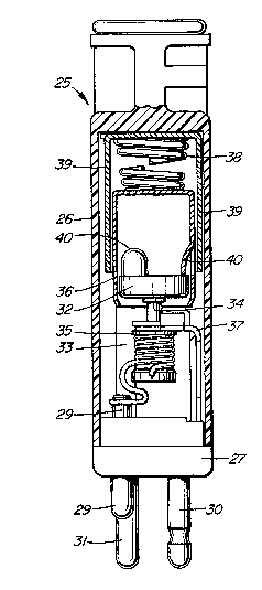
A packaged device, as described and illustrated, can be
manufactured suited to replace other protectors and to be retrofitted
to existing protector modules. Figures 8 and 9 illustrate the
application of protectors in accordance with the present invention in
one form of protector module. The module 25 is exemplary of protector
modules having two protectors for protecting both conductors of a
telephone line. It comprises a housing 26, open at its lower end, and
a base 27, attached to the lower end. Two pairs of line terminals 29
and 30 are provided in the base, plus a ground terminal 31. In the
example, there is both a primary overvoltage protector 32, which is of
the form as illustrated in Figure 5, and a heat coil unit 33, which is
in series in the telephone line between terminals 29 and 30. Heat
coil unit 33 has a central pin 34 soldered to the spool 35 of the heat
coil. On the occurrence of an overcurrent condition, or a sustained
overvoltage, the solder joint melts and the pin 34 moves down,
permitting a cup 36 to move down and contact a ground contact 37
connected to the ground terminal 31. This is conventional.
Normally positioned within the cup 37 is a carbon block
or a gas tube protector. Under an overvoltage condition, breakdown
5~:
across a gap in the protector occurs, thus providing a path from pin
34 through the protector to the cup 37, through spring 38 to ground
member 39, which is also connected to the ground contact 37. In the
example illustrated, the cup 36 has been modified by the forming of a
S number of indents 40, for example three. These indents are positioned
such that the protector 32 is held with the electrode 11 (Figures
1 to 5) in contact with the top end of the pin 34. The contact
surface of the electrode 11 is at the same level as would be the
contact surface of the electrode of a conventional protector. The
electrode 12 (Figures 1 to 5) of the protector 32 is in contact
with the indents 40 and thus in contact with the cup 37. Primary
protection for overvoltage surges is thus through the pin 34, through
protector 32, cap 36, spring 38, ground member 39 and ground contact
37. Overcurrent protection is as previously described, by melting of
a solder joint permitting movement of cup 36 down to contact the
ground contact 37.
Instead of indenting the cup 36, at 40, a normal cup
can be used, together with a spacer or a spring, to hold the protector
32 at the correct position.
The module 25 can be redesigned so as to take advantage
of the reduced height of the protector 32 as compared to a
conventional carbon block or gas tube protector. Cup 36 can be much
shorter, sufficient to house the protector. Such a reduction in
height can be particularly useful where two protectors are mounted in
line in a module, rather than slde-by-side as in the example.
Figures 10 and 11 illustrate two exemplary forms of
module specifically arranged to accommodate protector devices in
12
,
Z5~
accordance with the invent;on. Where practical, the same reference
numerals are used for items common with Figures g and 10. Figure 11
illustrates a module which includes a heat coil and Figure 12
illustrates a module without a heat co;l but with a fusible pellet.
As illustrated in Figure 10, the module Z5 has a
housing 26, open at its lower end, and a base 27 attached to the lower
end. Line terminals 29 and 30, and a ground terminal 31, are provided
in the base. In this example, there are both the primary overvoltage
protector 32 and a heat coil unit 33. The heat coil unit is in series
in the telephone line between terminals 29 and 30. The heat coil unit
has central pin 34 soldered to the spool 35 and on occurrence of an
overcurrent condition, or a sustained overvoltage, the solder joint
melts and the pin moves down, permitting cup 36 to move down and
contact ground contact 37, which is connécted to the ground terminal.
The difference between the arrangement of Figure 10 and
that of Figure 9 is that cup 36 in Figure 10 is considerably shorter
than in Figure 9. The cup need only be long enough to house the
protector 32. This enables the housing 26 also to be shorter.
Figure 11 illustrates a module 25 which does not have a
heat coil unit. It comprises housing 26, open at its lower end, and
base 27 attached to the lower end of the housing. The base has line
terminals 29 and 30 and ground terminal 31. The overvoltage protector
32, as in Figure 5, is positioned in cup 36. A pellet 45 is
positioned behind the protector 32 in the cup 36, the pellet being of
a fusible alloy. A shunt 46 connects the line terminals 29 and 30 and
a pin 47 extends up from the shunt and is in contact with electrode 11
(Figures 1 to 5) of the protector 32, The other electrode 12 (Figures
....
.
~ ~ .
S02
1 to 5) is in contact with the cup 36. On an overvoltage condition,
breakdown across the protector 3Z occurs, to the pellet 45, cup 36,
spring 38 and to the ground contact 37. In the event of a sustained
overvoltage condition, the pellet 45 melks and the cup 36 moves down
and contacts the ground contact 37.
The actuation of the examples in both Figure 10 and
Figure 11 is conventional, the difference being the use of solid state
protector 32, instead of a more usual carbon block or gas tube
protector. This enables a considerable reduction in height of the
complete module.
Figure 12 illustrates the application of the invention
to a further form of protector module, often referred to as a three
electrode module. The module comprises a housing 50 and a base 51
attaching to an open end of the housing. In the base are line
terminals 52 and 53, with a shunt 54 connecting each pair of line
terminals. Extending from each shunt is a spring cantilever contact
member 55. Also mounted in the base is a ground terminal 56 carrying
a contact member 57. At the end remote from the terminal 56, contact
member 57 is formed into a cylindrical shape 58, which is slotted at
59. Positioned in the cylindrical shape 58 is a protector 60.
Protector 60 comprises two solid state devices 61, as in Figures 1 to
5, back to back, with a central electrode 62 which fits into the slot
59. In this arrangement, effectively the electrodes 12 (Figures 1 to
5) are connected together. Two fusible pellets 63 are positioned one
on each side of the protector 60, making contact with electrodes 11
(Figures 1 to 5). When assembled, with ground terminal 56 in the base
51, the protector 60 and pellets 63 are also held between the free
14
.~, ' ~, ,`, '' .... ...
, .
1~;2S()~2
, ~
ends 64 of the cantilever contact members 55. Normal overvoltage
surges are shun~ed to ground by breakdown of one or both of the solid
state devices 61 to ground, to electrode 62, contack member 57 and
terminal 56. On a sustained overvo1tage condition, fusion of one or
both pellets 63 will enable one or both contact members 55 to contact
the ground member 57.