Sélection de la langue

Search

Sommaire du brevet 1292584 

Énoncé de désistement de responsabilité concernant l'information provenant de tiers

Une partie des informations de ce site Web a été fournie par des sources externes. Le gouvernement du Canada n'assume aucune responsabilité concernant la précision, l'actualité ou la fiabilité des informations fournies par les sources externes. Les utilisateurs qui désirent employer cette information devraient consulter directement la source des informations. Le contenu fourni par les sources externes n'est pas assujetti aux exigences sur les langues officielles, la protection des renseignements personnels et l'accessibilité.

Disponibilité de l'Abrégé et des Revendications

L'apparition de différences dans le texte et l'image des Revendications et de l'Abrégé dépend du moment auquel le document est publié. Les textes des Revendications et de l'Abrégé sont affichés :

  • lorsque la demande peut être examinée par le public;
  • lorsque le brevet est émis (délivrance).
(12) Brevet: (11) CA 1292584
(21) Numéro de la demande: 1292584
(54) Titre français: CIRCUIT DE SELECTION D'ANTENNE
(54) Titre anglais: ANTENNA SELECTION CONTROL CIRCUIT
Statut: Périmé et au-delà du délai pour l’annulation
Données bibliographiques
(51) Classification internationale des brevets (CIB):
  • H04B 07/08 (2006.01)
(72) Inventeurs :
  • LINDER, DONALD L. (Etats-Unis d'Amérique)
  • GOODE, STEVE HOWARD (Etats-Unis d'Amérique)
  • KAZECKI, HENRY LUDWIG (Etats-Unis d'Amérique)
  • DENNIS, DONALD WILLIAM (Etats-Unis d'Amérique)
  • BAKER, JAMES CLARK (Etats-Unis d'Amérique)
(73) Titulaires :
  • MOTOROLA, INC.
(71) Demandeurs :
  • MOTOROLA, INC. (Etats-Unis d'Amérique)
(74) Agent: GOWLING WLG (CANADA) LLP
(74) Co-agent:
(45) Délivré: 1991-11-26
(22) Date de dépôt: 1988-08-15
Licence disponible: S.O.
Cédé au domaine public: S.O.
(25) Langue des documents déposés: Anglais

Traité de coopération en matière de brevets (PCT): Non

(30) Données de priorité de la demande:
Numéro de la demande Pays / territoire Date
126,548 (Etats-Unis d'Amérique) 1987-11-30

Abrégés

Abrégé anglais


CM-00380H
ANTENNA SELECTION CONTROL CIRCUIT
Abstract of the Disclosure
An antenna switch control circuit for use in
achieving antenna selection diversity in TDM RF
receivers. RSSI for at least one antenna is monitored
during time slots containing information not of interest.
This information can then be compared with other antenna
performance information to allow a selection to be made
such that the receiver generally operates with the
antenna receiving the strongest signal. In one
embodiment, all possible antennas are monitored during a
time slot containing information not of interest. In
another embodiment, RSSI for the selected antenna can be
monitored during the time slot of interest, such that
antenna selection can again be varied should the selected
antenna diminish in performance.

Revendications

Note : Les revendications sont présentées dans la langue officielle dans laquelle elles ont été soumises.


- 8 - CM-00380H
We Claim
1. An antenna selection control circuit for use
with a TDM RF receiver having a least two antennas for
receiving an information signal, which information signal
is comprised of time slots of interest and other time
slots not of interest, comprising:
A) first means for developing signals related
to received signal quality for at least two of said
antennas, wherein said signal is developed for at least
one of said antennas during a time slot not of interest;
B) second means for comparing said developed
signals to identify which of said at least two antennas
received a signal of higher quality;
C) third means responsive to said second
means for causing said receiver to use said identified
antenna during a subsequent time slot of interest.

- 9 - CM-00380H
2. The antenna selection control circuit of
claim 1 wherein said first means develops said signals
for at least two of said antennas during a time slot not
of interest.
3. The antenna selection control circuit of
claim 1 wherein said signal quality comprises signal
strength.

- 10 - CM-00380H
4. An antenna selection control circuit for use
with a TDM RF receiver having a least two antennas for
receiving an information signal, which information signal
is comprised of time slots of interest and other time
slots not of interest, comprising:
A) first means for developing signals related
to received signal quality for at least two of said
antennas during a time slot not of interest;
B) second means for comparing said developed
signals to identify which of said at least two antennas
received a signal of higher quality;
C) third means responsive to said second
means for causing said receiver to use said identified
antenna during a subsequent time slot of interest.
5. The antenna selection control circuit of
claim 4 wherein said signal quality comprises signal
strength.

- 11 - CM-00380H
6. The antenna selection control circuit of
claim 4 wherein said first means includes sample and hold
means for sampling, during a first TDM time slot prior to
a TDM time slot of interest, a first signal related to
received signal quality from a selected one of said
antennas and for providing an output signal related to
said sampled signal.
7. The antenna selection control circuit of
claim 4 and further including:
A) fourth means for comparing, during said
next subsequent time slot of interest, a reference signal
with a signal related to received signal quality for said
selected antenna, and for providing a comparison output
signal related to said comparison; on; and
B) antenna switch control means for
responding to said fourth means output signal by causing
said receiver to select a different one of said antennas
for receiving said signal when said signal related to
received signal quality for said selected antenna is less
than said reference signal during said time slot of
interest.
8. The antenna selection control circuit of
claim 7 wherein said reference signal is related to a
mean value of received signal quality for said selected
antenna during said time slot of interest.

- 12 - CM-00380H
9. An antenna selection control circuit for use
with a TDM RF receiver having at least two antennas for
receiving an information signal, comprising:
A) sample and hold means for sampling, during
a first TDM time slot prior to a TDM time slot of
interest, a first signal related to received signal
strength from a selected one of said antennas and for
providing an output signal related to said sampled
signal;
B) comparator means for comparing, during
said first TDM time slot, said output signal from said
sample and hold means with a second signal related to
received signal strength from a different selected one of
said antennas, and for providing a comparator output
signal related to which of said antennas has received a
stronger signal: and
C) antenna switch control means for
responding to said comparator output signal by selecting
which of said antennas is used by said receiver to
receive the information signal in said TDM time slot of
interest.

- 13 - CM-00380H
10. The antenna selection control circuit of
claim 9 and further including:
D) reference signal means for providing a
reference signal related to a mean value of received
signal strength for said selected antenna during said TDM
time slot of interest;
E) second comparator means for comparing,
during said TDM time slot of interest, said reference
signal with a signal related to received signal strength
for said selected antenna, and for providing a second
comparator means output signal related to said
comparison;
F) second antenna switch control means for
responding to said second comparator means output signal
by causing said receiver to select a different one of
said antennas for received said signal when said signal
related to received signal strength for said selected
antenna is less than aid reference signal during said
TDM time slot of interest.

- 14 - CM-00380H
11. A method of selecting an antenna for a TDM RF
receiver having at least two antennas for receiving a
signal of interest, which signal is comprised of time
slots of interest and other time slots not of interest,
said method comprising the steps of:
during a time slot not of interest and
preceding a time slot of interest:
A) sampling and holding a signal related to
received signal quality for one of said
antennas;
B) comparing said sampled and held signal
with a second signal related to received
signal quality for a second one of said
antennas;
C) selecting, based upon said comparison one
of said antennas to be used to receive said
signal of interest in a next occurring time
slot of interest.

- 15 - CM-00380H
12. Ths method of claim 11 and including the
additional steps of:
during a time slot of interest that occurs
subsequent to said time slot not of interest:
D) monitoring a signal related to received
signal quality for said selected antenna;
E) comparing said monitored signal with a
reference signal;
F) in response to said comparison between
said monitored signal and said reference
signal, deciding whether to select a
different antenna.
13. The method of claim 12 wherein said reference
signal is related to a mean value of received signal
quality for said selected antenna during said time slot
of interest.
14. The method of claim 13 wherein in step F, a
decision is made to select a different antenna when said
monitored signal is less than 10 dB below said reference
signal.

Description

Note : Les descriptions sont présentées dans la langue officielle dans laquelle elles ont été soumises.


ANTENNA SELECTION CONTRO~ CIRCUIT
Background Art
Radio r2ceivers that make use o~ antenna
selection diversity are known in the art. In general,
such a receiver makes use of a default antenna, and only
makes use of the alternate antenna when the signal being
received by the default antenna diminishe~ below an
acceptable threshold (the threshold may either be a
preselected constant or a value that fluctuates somewhat
and represents, ror example, an average value of the
default antenna received signal). The criteria for
measuring antenna performance may be, for example, a
received signal strength indicator (RSSI).
Time division multiplexed (TDM) RF communications
systems are also known in the art. Such systems divide
information to be ~roadcast into packets, which packets
are then broadcast ln predetermined time slots. A typical
TDM system establishes a short time frame (for example, a
few milliseconds) made up o~ two or more time slots,
wherein the basic time frame format repeats continuously.
A typical receiver will monitor, decode, and process
further as appropriate information contained in time
slots of interest,:and receive but ig~ore information
contained in other time slots.
` 35

2~
- 2 - CM-00380H
A need exists to accommodate antenna selection
diversity in a TDM RF receiver.
Summary of the Invention
This invention includes circuitry Por developing
signals related to received signal quality, such as
signal strength, for at least two antennas associated
with a TDM receiver, wherein these signals are developed
10 for at least one of the antennas during a TDM time slot
not of interest. The circuit then compares these
developed signals to identify which of the antennas
receives the stronger signal, and caus2s the raceiver to
use that identified antenna.
In one embodiment, all of tha antennas associated
with the receiver are sampled during a time elot not of
interest, such that the antenna selection occurs prior to
receipt of a time slot of interest.
In another embodiment, the circuitry continues to
20 monitor received signal strength for the selected antenna
during the time slot of interest, such that if the
received signal strength diminishes unacceptably, the
receiver can be caused to utilize an alternative antenna
during the time ~lot of interest.
Brief ~ of the Drawinqs
Fig. 1 comprises a schematic diagram of a f i rst
- embodiment of the`invention;
Fig. 2 comprises a timing diagram associated with
the first embodiment;
Fig. 3 comprises a schematic diagram o~ a second
embodiment of the invention;

- 3 - CM-00380H
Fig. 4 comprises a timing diagram associated with
thQ second embodiment: and
Fig. 5 comprises a 3chematic diagram of
additional circuitry that can be utilizad with eithQr
embodiment.
_est Mode For Carrving Out The Invention
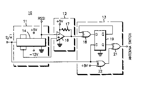
Referring now to Fig. 1, khe first embodiment can
bQ seen a~ depicted generally by the numeral 10. This
first em~odiment includes generally a sample and hold
circuit (11), a comparator (12), and an antenna ~witch
control circuit (13).
The sample and hold clrcuit (11) includes a
sample and hold device (14) such as an AD585. The sample
and hold control port connects to receive an appropriate
sample and hold control signal (S/not H) a~ described in
more detail below. ~he signal input port connects to
receive an RSSI signal. The output ports connect to the
comparator (12) as described below.
The comparator (12) can be comprised of a device
such as the MC3302 (16). The non-inverting input to this
devica connects to receive tha output of the sample and
hold device (14). The inverting input connects tc
rQaeive an RSSI siynal. The output of the device (16)
connects to a lK ohm pull-up resistor (17) and also to
onQ input o~ a first exclusive OR gate (18) that
constitutas one input to the antenna switch control
circuit (13).
The output of the first exclusive OR gate tl8)
connects to the data port of a flip-flop (19). The not Q
output of the flip-~lop (lg) connects to the remaining
input of the first exclusive OR gate (18). The Q output
of the flip-flop (19) connects to one input of a second
exclusive OR gate (21), the remaining input of which
connects to the output of a third exclusive OR gate (22).
One input of the latter connects to a positive 5 volt

~Z~tZ~
- 4 - CM-00380H
source and the remaining input connects to receive the
S/not ~ signal, which produces an inverted S/not H
signal, which signal also connects to the clock port of
the flip-flop (19). The output of the second exclusive
OR gate (21) constitu~es the antenna swi~ch output of the
antenna switch control clrcuit (13).
Referring to Fig. 2a, a ssrias o~ TD~ time slots
A and B can be seen, wherein slot A contains information
of interest and slot B contains information not of
interest to thQ receiver in question. Fig. 2b depicts
the S/not H signal that would correspond to this
arrangement. In particular, the S/not H signal as used
in the first embodiment depicted in Fig. 1 would cause
the sample and hold circuit (11) to sample RSSI for an
antenna during a time slot containing information of
interest. A comparison could then ba carried out during
time slots having information not of interest with
respect to the antenna actually being used. A
determination could then be ~ade as to which antenna
2Q should be used for subsequent time slots containing
information of interest.
Referring now to Fig. 3, an alternative
embodiment can be seen as depicted generally by the
numeral 30. This embodiment includes a sample and hold
circuit (11) and a comparator (12) essentially as
described above. Therefore, these particular sections
will not bo described again.
The second embodiment (30) also includes a
MC14013 ~lip-~lop (31) having its data port connected to
receive a CS2 signal a~ described below in more detail.
The clock port connects to rece~va an appropriate clock
signal as well understood in the art. The clock rate
should of course be chosen to acco~modate the time slot
and frame length durations of the TDM system in ques~ion.
The Q output of the flip-flop (31), which provides a
delayed version of the CS2 signal, connects to the
S/not H port of the sample and hold circuit (11). The
,'

~z~
- 5 - CM-00380H
not Q output of the flip flop (31) connects to the
antenna switch control circuit (32) as described below in
more detail.
Tha antanna switch control circuit (32) includes
a first exclusive OR gate (33) having one input connected
to receive the output of the comparator (12) and another
connected to receive the not Q output of a data type
flip-flop (34) associated therewith. The flip-~lop (34)
has its data port connected to rec~ive the output of the
first exclusive OR ga~e (33). The clock port o~ thl~
flip-flop (34) connects to receive a CS1 signal as
described below in more detail. ThiR CSl signal i~ also
provided to one input of a second exclusive OR gate (36),
the remaining input of which connects to a positive 5
volt source. The output of this exclusive OR gat~ (36)
connects to one input o~ an AND gate (37), thQ remaining
input o~ which connect~ to ~he not Q output of the ~irst
flip-flop (31) refsrred to above. The output of this AND
gate (37) and the Q ou~put o~ the ~econd flip-~lop (34)
connect to both inputs o~ a third exclusive OR gate (38),
the output of which connects to an appropriate antenna
switch as well unders~ood in the art.
Re~erring now to Fig. 4a, a series Or TDM time
slots A and B can again be se~n. An appropriate CSl and
CS2 control signal to be used in the second embodiment
(30) are d~picted in Figs. 4b and c. An S/not H control
signal that results through provision of these control
signals, in con~unction with an appropriate clock ~ignal,
is depicted in Fig. 4d.
By controlling the timing o~ the second
embodiment (30) as depicted in Fig. 4, the second
embodiment (30) will function to sample and compare RSSI
values for both antennas during time slots that are not
of interest, such that the decision regarding antenna
selectlon can be made prior to receipt of a time slot of
interest. With thi~ approach, an improvement can be
realized in a Rayleigh fading field with higher Doppler

S84
- 6 - CM-00380H
frequency where the time between an~enna samples and the
desired information slot is short.
Referring now to Fig. 5, an additional circuit
which can be used in combination with either embodiment
(10 or 30) can be seen as depicted generally by the
numeral 50. This circuit (50) functions to allow the
antenna in use during a time slot of interest to be
monitored and compared against a hi~torically determined
value of antenna performance. If instantaneou antenna
performance degrades sufficiently, this clrcuit (50)
caùse~ the receivar to switch antennas.
~ he circuit (50) depicted includes a reference
signal unit (51), a comparator (52~, and an antenna
switch control circuit (53).
Thq reference signal circuit ~51) receives an
RSSI signal for the antenna in u~e and, through use o~
the operational ampli~ier~ (54 and 55) and the lOK ohm
resistors and capaaitor depicted, develop~ an average
value for tho RSSI ignal with respect to time. The
variable resistor (50) connects to an appropriate 5 volt
sourca, and serves to SQt the level below mean at which
the circuit force3 a 3witch to the alternativ~ antenna.
The output of thi~ reference signal unit (51) connects to
the noninverting input of a comparator (52), thè
inverting input of which connect~ to receive an
instantaneous value representative of RSSI. The outpu~
o~ the comparator then connects to a 1~ ohm pull-up
resistor (56) and to on~ input of an AND gate (57) that
constitutes the input to the antenna switch control
circuit (53). The remaining input to the AND gate (57)
connects to receive a window trigger signal, which
essentially comprises the S/not H signal wherein the
leading edge is delayed by 0.5 milliseconds to
accommodate transients and to allow the circuitry to
reach steady state conditions (when using the embodiment
depicted in Fig. 3, tha window trigger signal can be
comprised of the CSl signal to achieve substantially thç

~Z~tZ5~39L
- 7 - CM-00380H
same effect). The output of the AND ga~e (57) connects
to the ~et port of a flip-~lop (58), the Q output of
which connects to one input of an exclu~ive OR gate (59),
the remaining input of which connects to ~he antenna
switch output of the antenna switch control circuit in
either embodiment (13 or 32). The output o~ this
exclusive OR gate (59) ~unctions to provide a signal that
can cause an appropriate an~enna ~witch to switch
antennas.
The reset port of the flip-flop (58) referred to
abova also connects to an appropriate re~Qt circuit that
includes a transistor (61) having a base connected
through an 18K oh~ resistor (62) to receive the window
trigger signal re~erred to above. The emitter of this
transistor connects to ground and ths collector connects
both to the reset port of the ~lip-flop (5a) and through
a 4.7K ohm resistor (63) to a po~itive 5 volt source.
The reset signal forces the antenna switch to be
controlled by the antenna switch control circuit (13 or
32) when the system receives a ~lot not of interest.
When recaiving the ~lot of interest, the antenna can b~
forcQd to ~witch to the alternative antenna by the
flip-Plop (58) based on ths comparator (52).

Dessin représentatif
Une figure unique qui représente un dessin illustrant l'invention.
États administratifs

2024-08-01 : Dans le cadre de la transition vers les Brevets de nouvelle génération (BNG), la base de données sur les brevets canadiens (BDBC) contient désormais un Historique d'événement plus détaillé, qui reproduit le Journal des événements de notre nouvelle solution interne.

Veuillez noter que les événements débutant par « Inactive : » se réfèrent à des événements qui ne sont plus utilisés dans notre nouvelle solution interne.

Pour une meilleure compréhension de l'état de la demande ou brevet qui figure sur cette page, la rubrique Mise en garde , et les descriptions de Brevet , Historique d'événement , Taxes périodiques et Historique des paiements devraient être consultées.

Historique d'événement

Description Date
Le délai pour l'annulation est expiré 2002-11-26
Lettre envoyée 2001-11-26
Accordé par délivrance 1991-11-26

Historique d'abandonnement

Il n'y a pas d'historique d'abandonnement

Historique des taxes

Type de taxes Anniversaire Échéance Date payée
TM (catégorie 1, 6e anniv.) - générale 1997-11-26 1997-10-03
TM (catégorie 1, 7e anniv.) - générale 1998-11-26 1998-10-07
TM (catégorie 1, 8e anniv.) - générale 1999-11-26 1999-10-04
TM (catégorie 1, 9e anniv.) - générale 2000-11-27 2000-10-03
Titulaires au dossier

Les titulaires actuels et antérieures au dossier sont affichés en ordre alphabétique.

Titulaires actuels au dossier
MOTOROLA, INC.
Titulaires antérieures au dossier
DONALD L. LINDER
DONALD WILLIAM DENNIS
HENRY LUDWIG KAZECKI
JAMES CLARK BAKER
STEVE HOWARD GOODE
Les propriétaires antérieurs qui ne figurent pas dans la liste des « Propriétaires au dossier » apparaîtront dans d'autres documents au dossier.
Documents

Pour visionner les fichiers sélectionnés, entrer le code reCAPTCHA :


Pour visualiser une image, cliquer sur un lien dans la colonne description du document. Pour télécharger l'image (les images), cliquer l'une ou plusieurs cases à cocher dans la première colonne et ensuite cliquer sur le bouton "Télécharger sélection en format PDF (archive Zip)" ou le bouton "Télécharger sélection (en un fichier PDF fusionné)".

Liste des documents de brevet publiés et non publiés sur la BDBC .

Si vous avez des difficultés à accéder au contenu, veuillez communiquer avec le Centre de services à la clientèle au 1-866-997-1936, ou envoyer un courriel au Centre de service à la clientèle de l'OPIC.


Description du
Document 
Date
(aaaa-mm-jj) 
Nombre de pages   Taille de l'image (Ko) 
Abrégé 1993-10-22 1 45
Revendications 1993-10-22 8 169
Dessins 1993-10-22 2 57
Description 1993-10-22 7 277
Dessin représentatif 2000-10-17 1 12
Avis concernant la taxe de maintien 2001-12-23 1 179
Taxes 1996-10-14 1 65
Taxes 1994-09-20 1 87
Taxes 1995-10-18 1 61
Taxes 1993-09-20 1 54