Note : Les descriptions sont présentées dans la langue officielle dans laquelle elles ont été soumises.
'78
- 1 - 45MR 00551
DIGITAL RADIO WITH SECURITY SYSTEM FOR SELECTIVE
ENABLING SOFTWARE CONTROLLED OPTIONS
FIELD OF THE INVENTION
This invention is related to digital radio
communications devices. More particularly, the
invention relates to radio communications device
security arrangements which permit a user to access
standard communications functions (as well as
additional "option" functions the user requests at time
of purchase of the radio) while preventing the user
from accessing additional "option" functions not
requested at time of purchase. Still more
particularly, the invention relates to software
controlled digital radio transceivers which perform
various functions under control of internally stored
program control instructions, and arrangements for
selectively enabling certain such functions and
inhibiting certain other such functions based on
security circuitry provided in the transceiver.
BACKGROUND AND SUMMARY OF THE INVENTION
For marketing and other reasons,
manufacturers of radio communications devices typically
offer several different configurations for each
communications product manufactured. A particular
model of mobile radio transceiver may have a "basic" or
minimal configuration by may optionally be provided
with additional features or "options" at additional
cost.
l~?Z~8
- 2 - 45MR 00551
For example, a basic transceiver
configuration may provide communications over a limited
number of communications channels for basic radio
transmitting and receiving functions required by all
users. Some users may, however, have additional
requirements requiring additional features -- such as
additional communications channels, receiver channel
scanning, public address capability, and tone activated
squelch. The ability of a manufacturer to provide such
additional "options" permits increases in the
flexibility, versatility, desirability and range of
applications of the product without penalizing
purchasers of the basic configuration with increased
cost. Purchasers of the basic model pay a minimum
price for the minimal configuration, while users
requiring additional "option" features pay an increased
price based on the number and type of options required.
In the past, additional options were
generally provided by incorporating additional
components and circuitry into the device. For example,
in the past channel scanning capability or additional
operating channels were added by installing additional
frequency selection circuitry into the transceiver.
Similarly, the tone activated squelch option typically
required an additional tone decoder circuit to be
installed. Transceiver designers used modular
architectures to accommodate additional plug-in "option
modules".
An example of this design approach is the
prior art "MLS" transceivers include basic transceiver
circuitry disposed within a housing. The front panel
assembly of the transceiver housing was manufactured
separately, and consists of a separable front panel
"escutcheon" plate. Mechanically mounted to the
escutcheon plate is a printed circuit board which
plug-connects to the basic transceiver circuitry when
l~Z~8
- 3 - 45MR 00551
the escutcheon plate is mechanically fastened to the
housing. The escutcheon plate and associated printed
circuit board comprises a module separable from the
transceiver main housing and basic circuitry. The
module includes user controls mounted on the escutcheon
plate and circuitry required to connect user controls
mounted on the plate to the transceiver circuitry.
Since different "option" features in many
cases require different additional user controls,
different models of escutcheon plate models were
produced for the "MLS" series transceivers. In
particular, the "MLS" transceiver was made available in
five different versions: (1) a two-channel "basic"
version; (2) an 8-channel version with the scan
feature; (3) a 16-channel version without scan; and (4)
a 16-channel version with scan feature. Five different
interchangeable escutcheon plates with different user
control arrangements corresponding to these five
different transceiver versions were also made. The
particular "MLS" transceiver limited the transceiver
features the user could access. For example, the
escutcheon plate corresponding to the "MLS" transceiver
version with 16-channel capability and no scan feature
does not have a control to actuate the scan feature --
preventing the user from obtaining the benefit of the
scan feature. Similarly, the escutcheon plates
corresponding to the 8-channel transceiver versions do
not include user controls to access more than 8
channels.
Since all "MLS" transceivers included
identical basic transceiver circuitry and main housing,
reduced manufacturing costs and increased reliability
derived from large scale manufacturing were obtained.
Specific purchaser selected options could be provided
in a particular unit simply by installing the
lZ~t2'778
- 4 - 45MR 00551
appropriate escutcheon plate module -- a procedure
which could be performed in the field if desired.
Incorporation of the circuitry performing the option
functions and user controls interacting with such
circuitry within the same front panel escutcheon plate
module permitted a transceiver to be reconfigured by
simply "unplugging" one module and "plugging in" a
different module (further increasing reliability and
decreasing manufacturing costs).
Digital microprocessor controlled radio
communications devices such as the "MLS" series
transceiver are generally known, or course. The
following (by no means exhaustive) listing of prior
issued patents is generally relevant to the state of
the art of so-called "digital radios":
U.S. Patent No. 4,378,55 -- Drapac - issued
March 29, 1983
U.S. Patent No. 4,392,135 -- Ohyagi - issued
July 5, 1983
U.S. Patent No. 4,525,865 -- Mears - issued
June 25, 1985
U.S. Patent No. 4,247,951 -- Hattori et al -
issued January 27, 1981
U.S. Patent No. 4,254,504 -- Lewis et al -
25 issued March 3, 1981
U.S. Patent No. 4,510,623 -- Bonneau et al -
issued April 9, 1985
U,S. Patent No. 4,688, 261 -- Killoway et al
- issued August 18, 1987
U.S. Patent No. 4,618, 997 -- Imazeki et al -
issued October 21, 1986
Such references teach controlling transceiver functions
in addition to transceiver operating parameters (e.g..,
operating frequencies) in response to digital signals
stored in a memory device.
- 5 - 45MR 00551
While older radio transceivers required
additional circuitry to perform additional, optional
functions such as channel scanning, tone activated
squelch and the like, modern digital microprocessor
controlled transceivers are capable of performing such
additional functions under software control with little
or no additional circuitry. For example, receiver
channel scanning can be implemented by providing an
enhanced receiver program control routine which
controls the microprocessor to periodically monitor
activity on various channels -- and additional
frequency data can be stored in a memory device to
provide additional transceiver operating channels.
Additional tone decoding and control algorithms
performed by the microprocessor under control of
additional program control software can provide
advanced squelch control functions, tone signalling
functions, and the like.
It would be unfair (and also poor marketing
strategy) to make users needing only a minimal
transceiver configuration pay for the high development
cost of advanced option features and enchancements.
Accordingly, for various reasons it is still very much
advantageous to offer the purchaser a "basic" lower
cost transceiver configuration while permitting him to
select additional option features at higher cost --
even though the main (or only) difference between the
basic and option configured transceivers may reside in
the specific program control routines they respectively
execute. This marketing strategy allows the
manufacturer to offer the basic unit at reduce cost and
at the same time requires purchasers requiring enhanced
operation to bear the additional costs associated with
developing and providing the additional option
features. For this marketing strategy to be
lZ~2'~78
- 6 - 45MR 005Sl
successful, however, purchasers of low cost basic
transceiver configurations must not be able to easily
modify their units to obtain more expensive option
features.
One possible way to obtain this result is to
provide different transceiver configurations, each
configuration including a different PROM (programmable
read only memory) storing only the subset of the
program control instructions and transceiver parameter
data associated with that specific configuration. This
approach has several disadvantages, however. One
important disadvantage is that field "upgrading" of a
transceiver is very difficult and time consuming, since
the transceiver has to be disassembled, the old PROM
removed, and a different PROM installed.
Commonly assigned U.S. Patent No. 4,525,865
to Mears discloses an arrangement whereby a
non-volatile memory within a mobile radio transceiver
can be reprogrammed without physical entry or removal
of components to provide the radio with additional
operational options (e.g., tone or digital addresses,
carrier control timers, or the like).
U.S. Patent No. 4,392,132 to Ohyagi and U.S.
Patent No. 4,378,551 to Drapac disclose security
arrangements for enabling and/or inhibiting option
features in paging receivers.
Ohyagi teaches an "information setter
circuit" comprising an 8X9 bit PROM in which is stored
"option selection bits" for selecting various
functional options of the paging receiver (e.g.,
automatic resetting after an alert, paging by
mechanical vibration in lieu of tone, and a battery
saving feature). The microprocessor reads the
information stored in this circuit as an input to the
program control algorithm it executes and enables or
inhibits the various option features accordingly.
The Drapac patent discloses discrete logic
lZ~ '8
- 7 - 45MR 00551
security circuitry incorporated as part of the paper
which connects with option selection circuitry
contained in a separable "code plug". The code plug
includes circuitry which controls tone decoding, and
additional simple fusible link type circuitry which
controls selection of various options such as batter
saving, automatic reset, and dual call operation.
Logic level signals a re connected through the fusible
links in the code plug to the security logic circuitry,
and the logic circuitry in turn enable or disables the
various options. The security logic circuitry detects
when a user tampers with the code plug fusible link
connections and prevents activation of the paging
device whenever tampering occurs.
While such arrangements may be satisfactory
in the context of a paging device, they do not readily
lend themselves to the more complex environment of a
full-feature digital radio transceiver -- in which many
more options may be provided and some additional
circuitry and user controls may be required to
implement the various options. In additional, greater
security than Drapac's code plug can provide is
necessary to prevent purchasers from successfully
enabling transceiver advanced option features through
tampering.
The present invention, like the prior art
"MLS" series radio transceivers described above,
provides different transceiver front panel escutcheon
plate modules for different optional transceiver
configurations. Unlike the prior art arrangement,
however, the present invention does not rely merely on
the absence of certain user controls to prevent a user
from accessing and operating "option" features of the
transceiver. In accordance with the present invention,
a security circuit is connected to communicate serial
l~Z'7'~'8
- 8 - 45MR 00551
data signals to and from a digital signal controller
(e.g., microprocessor) which is part of the main
transceiver circuitry. In the preferred embodiment,
the security circuit is a single chip programmable
logic array which implements certain Boolean logic
equations, the specific equations corresponding to a
specific option configuration.
The transceiver controller is capable of
performing any of various basic option functions under
control of program control instructions stored in a
non-volatile memory also part of the main transceiver
circuitry. The transceiver controller causes the
security circuit to generate a data byte in response to
signals provided by the controller, and enables and
disables transceiver "options" in response to the value
of the generated data byte.
In particular, upon initial application of
power to the transceiver, the controller transmits a
sequence of digital signals to the security circuit.
The security circuit permutes the sequence of signals
into a different sequence, the specific permutation
used being of arbitrary complexity -- and dependent on
transceiver "option" features to be enabled. The
security circuit communicates the permuted signal
sequence in serial form back to the controller. The
controller enables (executes) portions of the program
control instructions stored in its associated
non-volatile memory and disables (does not execute)
other portions of the stored program control
instructions in response to the sequence received from
the security circuit.
The protection against tampering provided by
the present invention is far greater than that provided
by any of the prior art arrangements described above.
This is in part because the security circuit must
respond to a serial data sequence which is fleeting and
12~?2~7 ~8
- 9 - 45MR 00551
in part because the permutation of that data sequence
performed by the security circuit can be an arbitrarily
complex function. Far more than mere grounding of pins
of a connector or the like would be required to defeat
the security circuit and its interaction with the
controller. Exact copying of the security circuit
might be necessary to duplicate the functionality of
the circuit in a form sufficiently miniaturized to be
physically disposed on an escutcheon plate.
These and other features and advantages of
the present invention will be better and more
completely understood by referring to the following
detailed description of presently preferred exemplary
embodiments in conjunction with the appended sheets of
drawings, of which:
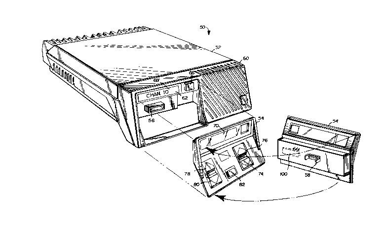
FIGURE 1 is an exploded perspective view of a
presently preferred embodiment of a digital radio
transceiver in accordance with the present invention
including an escutcheon plate module having a basic
control configuration;
FIGURES 2(A) through 2(F) are elevated front
views in plan escutcheon plate modules interchangeable
with the escutcheon plate module shown in FIGURE l;
FIGURE 3(A) is a schematic diagram of the
escutcheon plate modules shown in FIGURES 1 and 2(E);
FIGURE 3(B) is a schematic diagram of the
escutcheon plate modules shown in FIGURES 2(A)-2(D) and
2(F);
FIGURE 4 is a schematic block diagram of the
transceiver shown in FIGURE 1;
FIGURE 5 is a timing diagram of exemplary
signals exchanged in the preferred embodiment between
the transceiver and the escutcheon plate module; and
FIGURE 6 is a flowchart of exemplary program
control steps performed by the transceiver shown in
FIGURE 4.
l~Z~ ~ 8
- 10 - 45MR 00551
DETAILED DESCRIPTION OF THE PRESENTLY PREFERRED
EXEMPLARY EMBODIMENTS
FIGURE 1 is an exploded perspective view of a
presently preferred exemplary embodiment of a digital
radio transceiver 50 in accordance with the present
invention. Transceiver 50 includes a main module 52
and an escutcheon plate module 54. Main module 52 is
connected to escutcheon plate module 54 mechanically
via suitable conventional mechanical fastener and
electrically via a conventional mating multi-pin plug
56 (mounted on main module 52) and jack 58 (mounted on
escutcheon plate module 54). Escutcheon plate module
54 provides all user-operated controls for transceiver
50 except for power on/off switch 66, as will be
explained.
Main module 52 in the preferred embodiment,
includes front cap assembly 60, this front cap assembly
in turn including a display assembly 62 and an internal
speaker (not shown). Front cap assembly 60 is
interconnected to other circuitry within main module 52
by a conventional flat ribbon cable (not shown). A
microphone connector (not shown) is also provided at
the button of the front cap assembly 60. Display
assembly 62 in the preferred embodiment provides all of
the display indicators for transceiver 50, and also
includes a power on/off switch 66 which operates to
connect/disconnect power to/from main module 52.
Display assembly 62 is mounted on the front of front
cap assembly 60, with the display 68 being viewable
through a window 70 provided as part of escutcheon
plate module 54.
If desired, front cap assembly 60 and an
internal control board associated with it may be
separated from housing 72 of main module 52 and
installed in a remote control head for mounting under
vehicle dashboards and the like. If this alternate
1~2~'i8
- 11 - 45MR 00551
arrangement is used, a blank plate is mounted on main
module housing 72 in place of front cap assembly 60,
and escutcheon plate module 54 is connected to the
front cap assembly which in turn is mounted on the
remote control head.
In the preferred embodiment, transceiver 50
has certain "basic" operating functions (e.g.,
transmitting and receiving on at least two radio
frequency channels) but may also be equipped with
additional "option" functions such as multichannel
capability, external public address, and tone activated
squelch. In the preferred embodiment, identical main
modules 52 are used regardless of which options a
particular transceiver 50 is configured for. There are
seven different interchangeable versions of escutcheon
plate module 54 in the preferred embodiment -- and the
particular version of the escutcheon plate module which
is installed on a particular transceiver 50 determines
which option functions, if any, the transceiver is
capable of performing. In the preferred embodiment,
all that is necessary to reconfigure a particular
transceiver 50 to provide different option functions is
to remove its escutcheon plate module 54 and replace it
with a different version of the module.
The seven different interchangeable versions
of escutcheon plate module 54 provided in the preferred
embodiment are shown in FIGURE 1 and FIGURES 2A-2F.
Module versions 54(1) shown in FIGURE 1 is for the
"basic" transceiver configuration with no "option"
functions. This basic transceiver configuration
operates alternately on either of two different radio
frequency channels. User controls mounted on
escutcheon plate module version 54(1) include a channel
1 selector button 74, a channel 2 selector button 76,
volume up and volume down button 78, 80 and a "monitor"
("MON") button 82. A use of transceiver 50 provided
l~Z~7'~8
- 12 - 45MR 00551
with the "basic" escutcheon plate module version 54(1)
may select transceiver operations on either a
preassigned channel 1 or a preassigned channel 2,
increase or decrease speaker volume level, and select
5 between a muted mode and a monitor mode by manipulating
use controls 74-82.
The escutcheon plate module versions 54(2)
shown in FIGURE 2A enables transceiver 50 to perform
all of the basic functions permitted by module 54(1),
10 and adds the additional function of a "Type 99
decode". Additional use controls 84, 84 permit the
user to selectively (a) enable this decode function (by
depressing the "T99" control 84) and (b) reset the
decode function (by depressing "RSET" control 86). The
15 T99 decode option when enabled prevents the squelch of
transceiver 50 from opening except when a preprogrammed
2-tone signal is received.
Transceiver 50 equipped with escutcheon plate
module version 54(3) provides all of the basic
20 functions it would provide if equipped with escutcheon
plate module version 54(1) and, in addition, provides
multichannel and scan operation. More particularly,
the "channel 1" and "channel 2" controls 74, 76 of
escutcheon plate module version 54(1) now have "up
25 channel" and "down channel" functions, respectively,
and in addition, a "scan" control 88 is also provided.
A use may select any one of sixteen channels for
transceiver operation by operating control 74, 76, and
may also place transceiver 50 in a "scan" mode in which
30 the transceiver scans until it detects activity on one
of the sixteen preprogrammed channels and pauses on
(monitors) the active channel for the duration of
communications on that channel.
Escutcheon plate module version 54(4) shown
35 in FIGURE 2C is identical to version 54(3) shown in
FIGURE 2B except that versions 54(4) also provides
- 13 - lZ~Z 7 ~8 4sMR 00551
public address "option" function enabled by "PA"
control 90. Depression of PA control 90 routes the
audio output of an audio amplifier within front cap
assembly 60 to an external speaker output (not shown)
to provide public address operation.
Escutcheon plate module version 54(5) shown
in FIGURE 2D provides transceiver 50 with 128 channel
capability as well as scan operation. Controls 74, 76
perform the same functions in module version 54(5) as
they perform in version 54(3), but an additional "mode"
select control 92 is also provided in the version 54(5)
to select between logical groups of the 128 channels.
Escutcheon plate module version 54(6) shown
in FIGURE 2E provides 2-channel operating capability
and the public address "optional" function.
Escutcheon plate module version 54(7) shown
in FIGURE 2F provides 16-channel operation with scan in
addition to the T99 decode feature.
It will be understood from reviewing the
various "basic" and "Option" features provided by the
various interchangeable escutcheon plate modules 54
that in the preferred embodiment, three different
"option" features may be provided: (1) 2-channel verses
multichannel operation; (2) public address
capabilities; and (3) T99 decode squelch control. In
addition, the multichannel operation option has two sub
options: (a) 16-channel operation with scan; and (b)
128 channel operation with scan.
l~Z7'~8
- 14 - 45MR 00551
The following Table I summarizes the various
different "option" functions provided by transceiver 50
when connected to the various different interchangeable
escutcheon plate modules 54:
ModuleChannels Public Address T99 Decode
54(1) 2 no no
54(2) 2 no yes
54(3) 16 no no
54(4) 16 yes no
54(5) 128 no no
54(6) 2 yes no
54(7) 16 no yes
TABLE I
In the preferred embodiment, one of the
factors which determines the operational capabilities
of a particular transceiver 50 is the particular user
control configuration provided by the escutcheon plate
module version 54 installed on the transceiver -- just
as in the prior art "MLS" transceiver arrangement
discussed previously. For example, a transceiver 50
equipped with escutcheon plate module 54(1) does not
have public address capability because there is no user
control for selecting between internal and external
loud speaker (internal speaker is the default state).
Similarly, escutcheon plate module version 54(1) has no
controls for activating or resetting T99 decode squelch
control, and thus prevents the user from accessing this
feature of transceiver 50. However, if the
availability of user controls was the only mechanism of
transceiver 50 preventing the user from accessing
certain "option" functional characteristics (as it is
in the "MLS" transceivers), users might attempt to
modify or replace escutcheon plate module 54 so as to
add missing controls.
lZ~27'J'8
- 15 - 45MR 00551
In accordance with the present invention,
more than mere modification of the control
configuration is required to add "option" features to
transceiver 50. In particular, most of the escutcheon
plate modules 54 shown in FIGURES 1, 2A-2F, include a
security circuit 100 (shown in phantom in FIGURE 1)
which interacts with a digital controller within main
module 52 to enable or disable the multichannel and T99
decode squelch control option features of transceiver
50.
FIGURE 3A is an electrical schematic diagram
of escutcheon plate module versions 54(1) and 54(6) --
these two module versions lacking a security circuit
100. Various pins of jack 58 are connected to controls
74-82, 90. These pins are connected to ground when the
associated control is depressed (all controls of module
54 are momentary-on single-pole single-throw switches
in the preferred embodiment). In the preferred
embodiment, these pins are maintained at a logic level
1 signal level through pull-up resistors or the like.
The voltage potential on a pin is lowered to logic
level 0 whenever with switch 74-82, 90 connected to it
is depressed. Transceiver 50 senses changes in the
logic level of the various pins of jack 58 and responds
accordingly.
FIGURE 3B is a schematic diagram of
escutcheon plate module versions 54(2) - 54(5) and
54~7). In addition to various additional controls 84,
86, 88 (not shown in the FIGURE 3A schematic diagram),
these escutcheon plate module versions also include a
security circuit 100 which in the preferred embodiment
is a preprogrammed monolithic programmable logic array
("PAL") model P16R4 commercially available from MMI.
This PAL is a 20-pin programmable logic array with
latched outputs and implements "sum of products"
combinatorial logic -- thus providing a miniaturized
l~"Z7 ~8
- 16 - 45MR 00551
equivalent of a large array of discrete AND and OR
gates.
In the preferred embodiment, security circuit
100 is connected to the same pins of jack 58 to which
controls 74-92 are connected. Security circuit 100 in
the preferred embodiment processes data only upon
power-up of transceiver 50 (as will be explained in
greater detail shortly), and is therefore able to share
jack 58 pins with controls that are only operated after
power-up. In the preferred embodiment, the user should
no operate any of the controls mounted on escutcheon
plate module 54 until a few seconds after depressing
- power on/off switch 66 in order to give security
circuit 100 time to complete its data processing
functions and release the data lines connected to jack
58 for use as indicators of the states of controls
80-92. This dual function use of jack 58 increases
reliability and reduce manufacturing costs of
transceiver 50, since a 10-pin jack is all that is
required to electrically connect escutcheon plate
module 54 to transceiver main module 52.
Security circuit 100 pin 20 in the preferred
embodiment is supplied with power from jack 58 pin 5,
and pin 10 of the security circuit is grounded. A
clock synchronizing signal "CLK" is connected to jack
58 pin 6 (to which is also connected the "volume down"
control 80). Various enable input lines "OEx" at
security circuit pins 2-6 are connected to jack 58 pins
10, 9, 7, 3, and 2, respectively.
The :data in" (DIN) pin 18 of security
circuit 100 is connected to jack 58 pin 4 (to which is
also connected the "volume up" control 78), and the
security circuit "data out" (DOUT) pin 17 is connected
to jack 58 pin 8 (to which is also connected the
channel 1 or channel up control 74). Security circuit
100 enable (EN) pin 19 is connected back to the output
;8
- 17 - 45MR 00551
enable (OE) pin 11 of the security circuit; the "busy"
output at pin 16 is connected back to input A1 at pin
8; additional output "T99" at pin 15 in the preferred
embodiment is connected back to input A1 at pin 9; and
the load output LD at pin 14 is connected back to the
A3 input a pin 13. Pins 12 and 7 of security circuit
100 are not connected in the preferred embodiment.
The basic operation of security circuit 100
will now be described. Data input bits supplied to
security circuit data input DIN pin 18 (via jack 58 pin
4) are processed in sequence by a preprogrammed
combinatorial logic array equivalent within security
circuit 100, and outputs T99, LD, BUSY, DOUT, and En
are generated in response to the logic level present at
the DIN input and also in response to the signals
applied to input pins OEA, OEB, OEC, OED, OEE, Al, A2,
A3, and OE (some of these inputs being tied to latched
previous state outputs generated by the security
circuit). Data outputs available at security circuit
pins 14-19 are latched by internal latches within the
security circuit in response to edges of the
synchronization signal applied to the "CLK" input of
the security circuit -- so that the security circuit
output signal levels change only upon the occurrence of
a rising edge of the signal applied to the CLK input.
In addition, these outputs must be enabled by the
presence of signals on enable pins 2-6 in the preferred
embodiment.
The preferred mode of operation of security
circuit 100 is shown in the FIGURE 5 timing diagram.
An initial clock pulse Cl is applied to security
circuit CLK pin 1 in order to initialize the state of
the security circuit internal output latch. Then an
input signal level I is applied to the security
circuit DIN input and a short time late (this time
being sufficient to allow for gate propagation delays)
- 18 - ~ 27i8 4sMR 00551
the security circuit "CLK" input is clocked again to
latch the responsive outputs generated by the various
gate array equivalents in the security circuit. The
input level at security circuit input DIN is then
changed, and another clock pulse is applied to the CLK
input. This process continues for eight different
serial data input bits D1-D8 in the preferred
embodiment to produce eight corresponding output bits
01-08 at security circuit output pin DOUT. In the
preferred embodiment, each bit O is determined by the
value of the input bit I present at the DIN input of
security circuit 100 at the time a click pulse occurs,
and is also determined by the values present at
security circuit output pins 14-19 at that time. In
addition, the occurrences of data output bits O are in
corresponding timed relation with the occurrences of
clock pulses at jack 58 pin 6 in the preferred
embodiment.
The values of the output bits Ol-Oa are
determined by the Boolean logic which security circuit
100 has been preprogrammed to provide. In the
preferred embodiment, four different versions of
security circuit 100 are used to distinguish between
five different combinations of option features. These
different versions of security circuit 100 provide
identical programmable logic arrays P16R4 programmed
differently to provide different Boolean logic
functions. The following table summarizes the option
feature selection performed by the different security
circuits:
SECURITY CIRCUITCHANNELST99 DECODE
none 2 no
A 16 yes
B 128 no
C 16 no
D 2 yes
36
Z'~8
- 19 - 45MR 00551
In the preferred embodiment security circuit
type A is used to indicate 16-channel operation with
the T99 decode option feature, and is thus installed in
escutcheon plate module versions 54(7) shown in FIGURE
2F. Security circuit type B selects 128-channel
capability with no T99 decode, and is thus found in
escutcheon plate module version 54(5). Security
circuit version C selects 16-channel capability with no
T99 decode, and is found in escutcheon plate module
versions 54(3) and 54(4). Security circuit type D
selects 2-channel capability with the T99 decode
option, and is found in escutcheon plate module version
54(2). The absence of security circuit 100 selects no
T99 decode and only 2-channel capability (as is present
for escutcheon plate module versions 54(1) and 54(6) in
the preferred embodiment).
The only difference between security circuit
100 versions A, B, C and D in the preferred embodiment
is the way that they are programmed. Security circuit
100 in the preferred embodiment is programmed in a
conventional manner using a EPROM programmer with a
programmable logic array adapter. Those skilled in the
art understand how to program programmable logic arrays
such as those used in the preferred embodiment security
circuits 100 to implement Boolean logic quotations, and
no further discussion of the programming details is
therefore necessary. In the preferred embodiment,
security circuity 100 version A implements the
following set of "sum of products" Boolean logic
equations:
`` lZ~?Z7'78
- 20 - 45MR 00551
EN = NOT (OEA * OEB * OEC * OED * OEE)
LD = NOT (Al A2 A3 DIN +
Al A2 A3 DIN +
Al A2 A3 DIN +
Al A2 A3 DIN +
OEA OEB OEC OED OEE)
T99=NOT (Al A2 A3 DIN +
Al A2 A3 DIN +
Al A2 A3 DIN +
Al A2 A3 DIN +
OEA OEB OEC OED OEE)
_ _ _
BUSY=NOT (Al A2 A3 DIN +
Al A2 A3 DIN +
Al A2 A3 DIN +
OEA OEB OEC OED OED)
DOUT=NOT (Al A2 A3 DIN +
Al A2 A3 DIN +
Al A2 A3 DIN +
OEA OEB OEC OED OEE
EQUATION SET (A)
l~Z'7'7Y
- 21 - 45MR 00551
The Boolean logic equations implemented by
security circuit 100 version B is shown below:
EN = NOT(OEA OEB OEC OED OEE)
LD = NOT(A1 A2 A3 DIN +
Al A2 A3 DIN +
Al A2 A3 DIN +
Al A2 A3 DIN +
OEA OEB OEC OED OEE)
T99=NOT(Al A2 A3 DIN +
Al A2 A3 DIN +
Al A2 A3 DIN +
Al A2 A3 DIN +
OEA OEB OEC OED OEE)
BUSY=NOT(Al A2 A3 DIN +
Al A2 A3 DIN +
Al A2 A3 DIN +
Al A2 A3 DIN +
OEA OEB OEC OED OEE)
DOUT+NOT(Al A2 A3 DIN +
Al A2 A3 DIN +
Al ~ A3 DIN +
OEA OEB OEC OED OEE)
EQUATION SET (B)
~ ~2~?27';8
- 22 - 45MR 00551
Version C of the security circuit 100
implements the following Boolean equation:
EN = NOT (OEA OEB OEC OED OEE)
_ _ _
LD = NOT (A1 A2 A3 DIN +
Al A2 A3 DIN +
Al A2 A3 DIN +
OEA OEB OEC OED OEE)
T99=NOT (A1 A2 A3 DIN +
Al A2 A3 DIN +
A1 A2 A3 DIN =
OEA OEB OEC OED OEE)
BUSY=NOT (Al A2 A3 DIN +
Al A2 A3 DIN +
Al A2 A3 DIN +
OEA OEB OEC OED OEE)
DOUT=NOT (A1 A2 A3 DIN +
Al A2 A3 DIN +
A1 A2 A3 DIN +
Al A2 A3 DIN +
OEA OEB OEC OED OEE)
EQUATION SET (C)
2~ 8
- 23 - 45MR 00551
Security circuit version D is preprogrammed
to implement the Boolean logic equations shown below:
EN = NOT (OEA OEB OEC OED OEE)
LD = NOT (A1 A2 A3 DIN +
Al A2 A3 DIN +
Al A2 A3 DIN +
OEA OEB OEC OED OEE)
T99=NOT (Al A2 A3 DIN +
A1 A2 A3 DIN +
OEA OEB OEC OED OEE)
BUSY=NOT (Al A2 A3 DIN +
A1 A2 A3 DIN +
Al A2 A3 DIN +
OEA OEB OEC OED OEE)
DOUT=NOT (Al A2 A3 DIN +
Al A2 A3 DIN +
Al A2 A3 DIN +
A1 A2 A3 DIN +
A1 A2 A3 DIN +
OEA OEB OEC OED OEE)
EQUATION SET (D)
l~tZ71~8
- 24 - 45MR 00551
As can be seen from the Boolean logic
equations, each intermediate output LD, T99, BUSY, and
En in the preferred embodiment is formed by ORing
together a plurality of terms, each of these ORed terms
being formed by ANDing at least four inputs
(complemented or uncomplemented, depending upon the
term). One of the four inputs being ANDed in each term
is the serial data input bit DIN (complemented or
uncomplemented). The other three inputs are obtained
from outputs of the security circuit 100 itself. Each
gate array equivalent implemented by security circuit
100 in the preferred embodiment has its latched output
connected back to its input -- that is, the output
generated by a particular equation is dependent on the
previous output state generated by the same equation.
For example, the equations producing the LD output
include A3 input terms -- and the LD output is
connected to the A3 input of security circuit 100. One
of the equations implemented by each version of
security circuit 100 produces an output En which
requires all of inputs OEA, OEB, OEC, OED, OEE to be at
logic level zero in order for outputs DIN, DOUT, BUSY,
T99 and LD to be enabled (the EN output is connected
back to the output enable OE input); and each of the
other Boolean logic equations implemented by security
circuit 100 requires at least one of inputs OEA, OEB,
OEC, OED, OEE to be at logic level zero if the output
generated by that equation is to be responsive to DIN
and to the current output state of the security circuit
-- this feature preventing the security circuit from
generating outputs after "power-on" which might
interfere with the scanning of the states of controls
74-92.
Of course, security circuit 100 can implement
virtually any desired set of logic equations. For
example, a programmable logic element or other
- 25 - 1;~27~8 45MR 00551
programmable device could be used instead of the PAL
security circuit 100 in the preferred embodiment to
provide more complex logic. The PAL used in the
preferred embodiment provides only "sum of products"
5 logic with latched output. However, other programmable
devices are available which include additional
flexibility (so that, for example, the logic
implemented could be any combination of "sum of
products" and product of sums", and could even include
10 delays, storage elements or the like). The logic
equations implemented by security circuit 100 is some
function of its input (and also preferably some
function of its previous output) in the preferred
embodiment, and it is critical that the security
15 circuit always produces the same series of output when
simulated by a given series of inputs).
FIGURE 4 is a schematic diagram of transceiver main
module 52 in the preferred embodiment. Main module 52
includes a control microprocessor 130, a main module
20 processor 132, a "personality PROM" 138, a power supply
(or other source or power) 140, a multiplexer 142, and
a quartz crystal 144. Control microprocessor 130 sends
and receives data to/from main radio processor 132 via
serial data lines 146, 148. Schmitt triggered hex
25 inverters (not shown) are used to buffer these serial
lines to reduce noise and data error problems. Both
serial lines 146, 148 normally rest at plus 5 volts,
with data causing the lines to go low. Display 68 is
connected to an output port of control microprocessor
30 130, which converts serial data received from main
radio processor 132 into the data format needed tc
drive display 68. While power on/off switch 140, in
the preferred embodiment switch 66 momentarily grounds
a line which feeds conventional switching circuitry,
35 this conventional switching circuitry in turn
l~Z7 ~8 45MR 00551
connecting and disconnecting power supply 140 from the
circuitry of transceiver 50. In the preferred
embodiment, transceiver 50 is typically used in mobile
applications, so that power supply 140 is fed from a 12
volt dc source.
Plug 56 connects to control microprocessor
130 input port PA via lines which are normally pulled
high to plus 5 volts by 500K ohm pull-up resistors (in
the preferred embodiment, these resistors are part of
control microprocessor 130). A closure of any controls
74-92 of an escutcheon plate module 54 connected to
plug 56 grounds the corresponding input port line of
control microprocessor 130. Diodes on these lines
(shown schematically in FIGURE 4) protect control
microprocessor 130 from static discharges. Control
microprocessor 130 converts each switch closure to
serial data which it sends via serial data line 146 to
main radio processor 132 for appropriate response.
Control microprocessor 130 includes an
interrupt capability which causes the microprocessor to
execute a power-on interrupt routine (although a
conventional RC network 150 connected to an "INT" input
of the control microprocessor is shown in FIGURE 4, the
microprocessor may alternatively include internal
circuitry which causes it to "trap" to a power-on
interrupt "vector" when power is first applied to it).
FIGURE 6 is a flow chart of exemplary program control
steps performed by control microprocessor 130 when
power is first applied to it. This power-on interrupt
routine 160 is stored in the pre~erred embodiment in a
non-volatile memory 162 (which may be internal or
external to control microprocessor 130, and may
include, for example, a random access memory internal
to the microprocessor and a read only memory external
to the microprocessor). Memory 162 stores program
- 27 - 1 Z~ Z ~t8 45MR 00551
control instructions corresponding to power-on routine
160, as well as additional program control instructions
executed by control microprocessor 130 after power on
and during normal operation. In addition, memory 162
stores values X, YA, YB, YC and YD, and also stores a
flag called DECODE decode and a memory variable called
CHANNEL. The operation of control microprocessor 130
during power-on conditions will now be described in
connection with FIGURES 4-6.
Upon power-on, the first thing control
microprocessor 130 does in the preferred embodiment
(after possibly executing a "self test" routine) is to
apply a clock pulse to jack 56 pin 6 (which is
connected to security circuit 100 CLk pin 1 if an
escutcheon plate module 54 with a security circuit is
installed) (block 164). In the preferred embodiment,
control microprocessor 130 generates clock pulses at
its CLK output pin at a frequency determined by quartz
crystal 144, these clock signals being used to
synchronize other devices connected to the
microprocessor. In the preferred embodiment, jack 56
pins 6 is usually used to sense the state of "volume
down" control 80, and therefore should not always be
connected to the control microprocessor clock signal.
Multiplexer 142 (which may comprise either a hard-wired
external discrete multiplexing device or a
software-controlled multiplexer equivalent implemented
by control microprocessor 130) applies microprocessor
clock pulses to jack 56 pin 6 only during power-up (as
is shown in FIGURE 5). Control microprocessor 130
causes jack 56 pins 10, 9, 7, 3, 2, 4 to all be a
appropriate predetermined logic levels upon application
of the first clock pulse to security circuit 100 so
that the security circuit output is forced into a
predetermined desired initial output state.
- 28 - 1~2~ 4sMR 00551
Control microprocessor 130 then applied a
data bit I (e.g., the first bit of an 8-bit X value
stored in memory 162) to the security circuit 100 DIN
input (via jack 56 pin 4) (block 166). As described
previously, the application of an input bit causes the
logic array implemented by security circuit 100 to
respond by applying resulting data bits to its internal
output latch input. After a gate propagation delay
time has passed, control microprocessor 130 again
clocks security circuit 100 (via jack 56 pin 6) to
latch that data into the security circuit output latch
(block 168). Control microprocessor 130 then reads the
data bit security circuit 100 has latched at its DOUT
output (via jack 56 pin 8) and stores that bit into an
internal microprocessor register (block 170). Control
microprocessor 130 then accesses the next bit of the
predetermined memory value X stored in memory 162. If
bits remain in this memory constant which have not yet
been applied to security circuit 100 (block 172),
blocks 166-172 are repeated for the remaining bits of
memory constant X (to apply input bits I -I to security
circuit input DIN and to receive and store the
resulting security circuit outputs O -O ). Nemory
constant X may be of arbitrary length, but in the
preferred embodiment it is eight bits long so that by
the end of this process control microprocessor 130 has
stored in its internal register an 8-bit long output
value O -O which it has received in serial fashion
from security circuit 100 in response to (a) and 8-bit
input value sent to the security circuit, and (b) the
security circuit initial state.
Control microprocessor 130 then compares the
output byte O obtained from security circuit 100 with
four different values stored as constants YA, YB, YC
and YD>
If the string of output bits received from
- 29 - 1 25,~ ~845MR 00551
security circuit 100 is identical to the string of bits
YA (as tested for by decision block 174), security
circuit 100 has been programmed to implement equation
set (A) and is therefore part of escutcheon plate
module version 54(7). Control microprocessor 130 sets
the DECODE flag to YES and sets the CHANNEL variable to
16 (block 176).
If decision block 174 reveals that the value
returned by security circuit 100 is not equal to the YA
value, decision block 178 tests whether this return
value is equal to constant YB. If so, then security
circuit 100 has been preprogrammed to implement
equation set (B) and is therefore part of an escutcheon
plate module version 54(5)> Control microprocessor 130
sets the DECODE flag to no and sets the CHANNEL memorv
variables to 128 (block 180).
If the value returned by security circuit 100
is equal to constant YC, on the other hand (as tested
for by decision block 182), security circuit 100
implements the equation set (C) and thus corresponds to
escutcheon plate module version 54(3) or 54(7). In this
instance, control microprocessor 130 sets the CHANNEL
variables to 16 and sets the DECODE flag to NO (block
184).
Finally, if the test of decision blocks 174,
178 and 182 have all failed, the value received from
security circuit 100 is compared with the value of
constant YD (decision block 186). If decision block
186 reveals that the data returned by security circuit
100 is identical to the constant YD, then security
circuit 100 must implement equation set (D) and must
therefore be part of an escutcheon plate module version
54(2). Control microprocessor 130 sets the CHANNEL
variable to the value of 2, and sets the DECODE flag to
yes.
1 ~ ~2 77~45MR 00551
If the tests of all the blocks 174, 178, 182
and 186 fail, then no options are enabled and
microprocessor 130 sets the CHANNEL variable to the
default value of 2 and the DECODE flag to default
value of no (block 190). Various conditions may
cause all these tests to fail. Once such condition is
that no security circuit 100 is connected to jack 56.
As is shown in FIGURE 3A, escutcheon plate module
versions 54(1) and 54(6) do not include a security
circuit 100. If no security circuit 100 is present,
the value read by block 170 will all be at logic level
1 in the preferred embodiment and will not correspond
to any of constants YA-YD. Another condition that
could cause all these tests to fail is that the
security circuit 100 is malfunctioning or is partially
disconnected (a possible indication of tampering).
Because tests 174, 178, 182, 186 are very strict (i.e.,
the value returned by the security circuit 100 must
exactly match one of four expected values and must be
in timed relation with the occurrence of clock pulses
generated by control microprocessor 130), only a
circuit which returns precise expected values at the
correct times will satisfy the tests.
An important feature of the invention is that
security circuit 100 responds to a changing input
value. While security circuit 100 returns the same
output value string for a given input value string, it
will return a different (but expected and predictable)
output value showing for a different given input value
string. In accordance with the present invention, the
input string value X stored in memory 162 is not known
by the user and cannot be predicted by the user. While
it might be possible to analyze signals produced by
transceiver 50 in order to determine what that X value
is for a particular transceiver, different serial
~2'7~
- 31 - 45M~ 00551
numbers of transceiver 50 could store different X
values -- so that a simplified security system 100
designed to return a particular fixed value each time
it is clocked might only work for one specific
transceiver 50. If desired, transceiver 50 can even
change the value X it uses on successive power-ups.
For example, transceiver 50 could calculate (using a
random or pseudo-random process) a new input string
value X upon each power-up, calculate the expected
value to be returned by equation sets (A)-(D), and use
those calculated values as constants YA-YD,
respectively. In this particular arrangement, it would
not be possible for someone to defeat the security
provided by security circuit 100 by merely replacing
the security circuit with, for example, a programmable
shift register which would load and shift a constant
value in response to clock pulses received from main
module 52.
In the preferred embodiment, the values
stored in the channel variable and the DECODE flag are
communicated via serial data line 146 to main radio
processor 132. These values are used to selectively
enable or disable portions of programming stored in
read only memory 139. In the preferred embodiment,
conventional program control instructions stored in ROM
139 include alternate routines accessed via branching
dependent upon the DECODE and CHANNEL values returned
by control microprocessor 130. For example, the
conventional channel control portion of the control
algorithm stored in ROM 139 reads frequency allocation
values stored in personality PROM 138 and controls
transmitter 134 and receiver 136 to operate on a
specific frequency pair (channel) selected from
personality PROM 138 data in response to signals
present on jack 56 pin 6 (channel down) and pin 8
lZ~Z'7'78
- 32 - 45NR 00551
(channel up) after power-up routine 160 has completed
and control microprocessor 130 begins executing a
conventional main routine which simply senses (scans)
the state of the various pins of jack 56 and returns
corresponding encoded values to main radio processor
132. In the preferred embodiment personality PROM 138
is a read/write memory device than can be programmed by
an equipment dealer using an appropriate conventional
GE radio programmer. A portion of personality PROM 138
is set aside to store data corresponding to up to 128
different radio frequency channels. Main radio
processor 132 only accesses as many channels as is
indicated by the value of the CHANNEL variable sent to
it by control microprocessor 130, however. That is, if
the CHANNEL variable has a value of 2, main radio
processor 132 only accesses two different channels
stored in personality PROM 138 at predetermined storage
locations in the personality PROM and totally ignores
all other channel data stored in the personality PROM.
Thus, even if a dealer were to program personality PROM
138 with all of the data necessary for 128 channel
operation and the T99 decode function, the particular
security circuit 100 (or absence of it) in the
escutcheon plate module 54 would prevent main radio
processor 132 from using all but the specific data
stored in personality PROM 138 corresponding to the
options enabled by the escutcheon plate module.
While the invention has been described in
connection with what is presently considered to be the
more practical and preferred embodiments, it is to be
understood that the invention is not to be limited to
the disclosed embodiment, but on the contrary, is
intended to cover various modifications and equivalent
arrangements included within the spirit and scope of
the appended claims.