Note : Les descriptions sont présentées dans la langue officielle dans laquelle elles ont été soumises.
1~2 t~
DETECTOR AND MIXER DIODE OPERATIVE AT ZERO BIAS
VOLTAGE AND FABRICATION PROCESS THEREFOR
Technical Field
This invention relates generally to semiconductor
diode detectors useful for microwave and millimeter wave
applications, and more particularly to such detectors which
are operative at high detection efficiencies with zero bias
voltage Additionally, the multi-functional structure of
the diode detector disclosed and claimed herein is unique`~y
adapted to operate in the anti-parallel mixing mode with an
identical reversely poled structure to form a highly symmet-
rical mixer diode pair, also operable with zero volts bias
and subetantially free o~ odd order harmonic mixing pro-
ducts
In the field of microwave and millimeter detec-
tion, it i8 a common practice to provide a predetermined
bias voltage on a semiconductor diod- in order to set the DC
operating point on a nonlln-ar reglon Or the diode's
current-voltag- ~-V) characteristic in order to provide for
maximum det-ction effici-ncy ~ypically, this DC bias vol-
tage ls on th~ ord~r o~ 0 7 volt~ wher~ th- dlode is highly
conductive in a range on on- ~ide oS tho DC bias voltage
polnt and ratherlightlyconductive in a range on the other
side of this DC bias voltag-
There are, howevor, several signi~icant disadvan-
tages in the requirement for a DC bia~ voltage on the diode
detector First, the requirement per se of DC bias circuitry
between a power supply and the detector diode adds cost and
complexity to the detector arrangement Secondly, there is
a certain amount of noise associated with the DC bias vol-
tage, and this noise degrades the senRitivity and decreases
the dynamic range of the detection Thirdly, the bias
voltage is thermally sensitive and will therefore frequently
cause the DC bias operating point on the diode~s I-V charac-
l~?Z~O~
teristic to be shifted in response to changes in ambienttemperature at the DC bias source.
Similarly, when employing mixer diodes, it has
been a common practice to provide a DC bias voltage across
the mixer diode or diodes in order to establish a desired
operating poin~ on the I-V characteristic of these diodes.
one such mixer diode structure is disclosed for example by
Malik in U.S. Patent 4,410,902. However, an additional
problem in the Malik mixer structure arises from the fact
that there will be some extraneous and undesirable doping in
the body of the Malik structure from impurities in the
substrate moving upwardly into the epitaxial layers thereon.
This doping results in an unevenly distributed and extra-
neous impurity profile across these layers, and this profile
in turn produces dissimilar and asymmetrical I-V curves in
the first and third quadrants of the device's comosite I-V
characteristic. Such as~vmmetrical I-V characteristics ulti-
mately result in the generation of unwanted odd harmonic
signals of the fundamental mixing frequency.
For a further discussion of this problem of extra-
neous doping in mixer structures of the type disclosed by
Malik in U.S. Patent 4,410,902, reference may be made to an
article by S. C. Palmateer, et al., entitled "A study of
substrate eftects on planar doped structures in gallium
arsenide grown by molecular beam epitaxy",In~ te Phvsics
Conf~L~nQ~, Serial Number 65: Chapter 3, presented at the
International Symposium of Gallium Arsenide and Related
Compounds, Albuquerque, New Mexico, 1982, at page 149 et
seq.
In the field of diode detection there has been at
least one attempt to provide a detector diode which operates
with zero bias. Such an attempt is evidenced for example in
U.S. Patent 3,968,272 issued to Anand. However, the Anand
device relies upon the reaction of a semiconductor surface
with certain metals in a controlled manner. It is well
known that such semiconductor surface chemistry is difficult
to control and this fact will in turn affect device yields
and repeatability of results. Additionally, using the Anand
?2809
process stable barrier heights have only been demonstrated
in silicon which has a lower electron velocity than gallium
arsenide, and thus operates at slower speeds than GaAs.
Also, silicon has a higher parasitic capacitance than GaAs,
a fact which further contributes to the slower speeds of
silicon devices.
Disclosure of Invention
The general purpose of the present invention is to
provide a new and improved detector diode which is operative
at zero volts bias with a high detection efficiency and
which therefore overcomes the aforedescribed disadvantages
of the prior art. An additional purpose of this invention
is to simultaneously provide a diode structure which is
uniquely suited and adapted to operate with an identical,
reversely poled diode structure in an anti-parallel mixing
mode, having a highly symmetrical I-V characteristic and
substantially free o~ odd order harmonic generation. Thus,
this multi-functional diode structure may advantageously be
constructed in a single wafer fabrication process which, in
a preferred embodiment, employ~ molecular beam epitaxial
growth to achieve high quality, high purity, and high thick-
ness control in the multiple epitaxial layers. The resul-
tant diode structure may be operated either a~ an ef~icient
detector diodo, or it m~y be connected in the anti-parallel
mode with an identical mixer diode to exhibit a highly
symmetrical compo~ite I-V characterisitic nece~sary for the
prevention of odd harmonic frequency generation.
To accomplish the above purposes, I have dis-
covered and developed a new and improved diode structure
which includes an intrinsic or substantially intrinsic (or
lightly doped) layer of semiconductor material of predeter-
mined thickness upon which a thin critical layer of one
conductivity-type semiconductor material is epitaxially
formed sufficiently thin so that it is fully depleted of
majority carriers therein. The intrinsic (or lightly doped)
layer must also be substantially depleted of majority car-
riers in order to provide optimum symmetry of the I-V char-
~2~0~
acteristic of the structure. An additional layer ofopposite conductivity-type semiconductor material is
epitaxially formed adjacent the thin critical layer and
should be of sufficient thickness and impurity
concentration so that it is not fully depleted of
carriers during operation. This layer also provides a
good barrier between an outer ohmic metal contact and
the thin critical epitaxial layer of the one
conductivity-type. Preferably, all of the above layers
lo are formed on a substrate layer in successive steps of
controlled molecular beam epitaxy.
Various aspects of this invention are as
follows:
A diode structure operative at zero volts DC
bias to provide both good detection efficiency in diode
detector applications and to provide good harmonic
suppression in anti-parallel mixer diode applications,
comprising:
a. a single intrinsic or substantially intrinsic
semiconductor layer of a predetermined thickness
and impurity concentration and substantially
depleted of majority carriers;
b. a critical thin layer of one conductivity type
disposed on one surface of said intrinsic layer and
being sufficiently thin and of an impurity
concentration level sufficient so that it is also
substantially depleted of ma~ority carriers at zero
volts DC bias, said intrinsic layer being disposed
on only one surface of said critical thin layer:
c. a layer of opposite conductivity type
semiconductor material disposed on the surface of
said critical thin layer and of a thickness
sufficient to shield metal impurities from said
critical thin layer;
d. a first ohmic contact on said layer of
?2~0~
4a
opposite conductivity type semiconductor material:
and
e. a second ohmic contact disposed on either a
conductive substrate member or a semiconductor
substrate member, either of which is in electrical
contact with said intrinsic layer, whereby the
potential barrier height of said structure, ~B~
when multiplied by the charge on an electron, -q,
is established at a minimum value somewhere between
zero electron volts and the bandgap energy of the
semiconductor material of said layers.
A process for fabricating a diode structure
which may be operated with good detection efficiency at
zero volts DC bias in diode detector applications or
which may alternatively be operated as a mixer diode
free of odd order harmonic mixing products, also at zero
volts DC bias, in anti-parallel mixer diode
applications, including the steps of:
a. providing a single intrinsic or substantially
intrinsic semiconductor layer of predetermined
thickness and impurity concentration and
substantially depleted of ma~ority carriers;
b. epitaxially depositing a critical thin layer
of one conductivity type on one surface of said
intrinsic layer and being sufficiently thin and of
an impurity concentration level sufficient to
insure that this layer is also substantially
depleted of ma~ority carriers at zero volts DC
bias, said intrinsic layer being disposed on only
one surface of said critical thin layer;
c. depositing a layer of opposite conductivity
type semiconductor material on the surface of said
critical thin layer and of a thickness sufficient
to shield metal impurities from said critical thin
layer:
lZ!3Z~
4b
d. depositing a first ohmic contact on said layer
of opposite conductivity type semiconductor
material; and
e. depositing a second ohmic contact on either a
conductive substrate member or a semiconductor
substrate member, either of which is in electrical
contact with said intrinsic layer, whereby the
potential barrier height of said structure, ~B~
when multiplied by the charge on an electron, -q,
is established at a minimum value somewhere between
zero electron volts and the bandgap energy of the
semiconductor material of said layers.
A semiconductor device structure of either
NPIN or PNIP layered configuration and having a minimum
potential barrier height which, when multiplied by the
charge on an electron, -q, is a value between zero
electron volts and the semiconductor bandgap energy,
characterized in that the I or intrinsic layer is
depleted or substantially depleted of majority carriers,
said intrinsic layer being disposed on only one surface
of the interior P or N layer, and the interior P or N
layer adjacent to the intrinsic layer is between 25 and
140 Angstroms in thickness and also depleted of majority
carriers at zero volts DC bias.
The above purposes, advantages, and other
novel features of this inventlon will become better
understood in the following description of the
accompanying drawings wherein:
Brief Description of the Drawings
Figures lA and 18 illustrate the basic
structural configuration of the novel detector/mixer
diode according to the invention.
Figures 2A and 2B illustrate the majority
carrier potential barrier extending across the various
layers of the diode.
9Z~30~
4c
Figures 2C and 2D illustrate the increasing
majority carrier potential across the diode structure of
Figure 2A for forward bias and reverse bias conditions,
respectively.
Figures 3A through 3D illustrate respectively
four (4) alternative structural embodiments of the
invention wherein either the exact position or the
conductivity type of the thin critical layer are
different in each structure, but are operative to
functionally accomplish the same detection or mixing
function to be further described.
Figures 4A and 4B show a diode detection
network (and associated I-V characteristic) utilizing
the diode according to the invention.
Figures 5A and 5B show an anti-parallel diode
mixer pair (and associated I-V characteristic) for the
mixer diode according to the invention.
1~9~09
Best Mode For Carryina Out The Invention
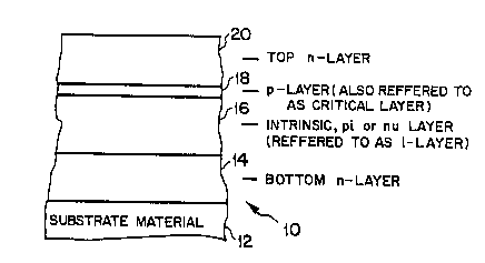
Referring now to Figures lA and lB, the diode
structure is indicated generally as 10 and includes a semi-
insulating gallium arsenide (GaAs) substrate 12 which is
typically 107 to 1o8 ohm-centimeters in resistivity and 8 to
10 mils in thickness. An N type epitaxial layer 14 is depo-
sited on the substrate 12 and is typically 5000 Angstroms in
thickness and has a doping concentration of about 1ol8
silicon dopant atoms per cubic centimeter. The next layer
16 is an intrinsic or "I" layer of approximately 3000 Ang-
stroms in thickness and typically ha~ a doping concentration
of about 1014 dopant atoms per cubic centimeter.
The intrinsic layer 16 has a thin P type layer 18
of epitaxial material depos~ted on its upper surface, and
the P type layer 18 is also referred to herein as the criti-
cal layer. This layer 18 may range in thickness between 25
and 140 Angstroms, but will normally be about 40-50 Ang-
stroms in thickness, and thus ~ufficiently thin so as to be
fully depleted of minority carriers (or electrons) in this
structure. The dopant concentration of layer 18 will be
about 8X10¹⁸ beryllium atoms per cubic centimeter. A top N
type layer 20 is epitnxially deposited as shown on the top
surface of P type layer 18, and this upper layer 20 will
typically be about 3000 Angstroms in thickness and will have
a carrier ConCentr~tion of about 5X10¹⁸ silicon atoms per
cubic centimeter.
The type of semiconductor material of the struc-
tures des¢ribed herein is not critical, and 6uch type only
determines the potential barrier height range that can be
achieved for these structures which are all formed prefer-
able using molecular beam epitaxial (MBE) deposition proces-
ses. Such known and commercially available computer con-
trolled MBE processes are preferred in that they are pre-
sently capable of providing the best repeatable layer thick-
ness control and doping uniformity of any presently avail-
able epitaxial processes. Although the critical layer 18
may range in thickness from 25 to 140 Angstroms, it is pre-
ferred that it be 40 to 50 Angstroms in thickness, with a
1~9Z~309
maximum acceptable tolerance of + 5 Angstroms
In the MBE best mod~ process used in constructing
the devices disclosed and claimed herQ, both silicon and
beryllium were alternated in the MBE epi system for N and P
type doping respectively
The presently known best modQ for carrying out the
MBE epitaxial deposition according to the invention is the
use of an epitaxial reactor known in the trade as the VARIAN
GEN-2 available ~rom VARIAN ASSOCIATES of Palo Alto, Cali-
fornia, with M3E shutter control provided by a Hewlett
Packard HP1000 computer For convenience, a summary table
of tho various layor thickne~ or thickness rang- and doping
level~ is given below ~or the devlce ~tructure of Figure lA
It will be understood, however, that these doping levels and
thickne~ apply equally to corre~ponding layer~ of the de-
vice~ sub~oquently de~cribod with ref-renc- to Figures 3A-
3D
14 5000 A 1018~ilicon atoms/cc
16 3000~ 1014atom~/co
18 2S-140 A 8x10¹⁸B- ~tom8/cc
3000 A 5xl018-ilicon atoms/cc
For a furth-r di~cus~ion of thi8 MBE technology,
referenc- may be mad- to Proceeding~ Q~ Ei~h_ Molecular
Beam Epitaxy Works~o~ edited by John R Arthur, attended 6-7
October, 1983, Georgia In~titute of Technology, Atlanta, Ga
and published rOr th- American Vacuum Society by the Ameri-
can Institute of Physics, New York 1984
The semiconductor device o~ Figure lA ha~ elec-
trons as its ma~ority carrierg, but if N layers are changed
to P layers and vicQ versa, th~ ma~ority carriers become
holes Ohmic or non rectifying contactg 22 and 24 are made
to the N type layer~ 20 and 14 respectively in Figure lA,
and the diodQ structure ig etched in a mesa-like configura-
~Z9~
tion with the side wall contours shown and isolated physi-
cally on the N layer 14 from the ohmic contact 24. However,
if a conducting substrate 12 is used instead of a semi-
insulating substrate material, then the N layer 14 can be
omitted and the intrinsic layer 16 positioned directly atop
the proposed or alternative conductive substrate material
(not shown). The exact mesa type con~iguration of the NPI
structural portion of Figure lB may be determined by mesa
etching, ion milling or other similar known processing me-
thods.
The proper thickness and doping levels of the
above described semiconductor layers of the diode structure
are essential to optimum device operation. The top layer 20
needs to be thick enough so that it is not fully depleted of
majority carriers during operation, and it also must be
sufficiently thick to provide an adequate barrier between
the ohmic contact 22 (which diffuses partially into the top
N layer during alloying) and the thin critical P layer 18.
If the N layer 20 doping level is sufficiently high, non
alloyed contacts can be utilized and the diffu~ion of the
metal will not be a problem. The thickne~s and impurity
doping level of the P type layer 18 and the impurity doping
level in the top N layer 20 are all determinative of the
height of the potential barrier at the PN ~unction between
layer~ 18 and 20. This condition is quite different from
the planar doped barrier diode of the above identified Malik
U.S. Patent 4,410,902 where the potential barrier height is
determined by the P layer doping, the P layer thickness and
the thicknesse~ of the two ~2) intrinsic layers used there-
in. The P layer 18 in FigurQs lA and lB needs to be suffi-
ciently thin so that it is fully depleted of majority carr-
iers, and the intrinsic or lightly doped layer 16 must be
appreciably depleted of majority carriers so as to give
optimum asymmetry to the I-V characteristic of the diode.
The thickness and doping level of the bottom N
layer 14 is not critical as long as a good ohmic contact can
be made to this layer and as long as the layer 14 is thick
enough and sufficiently doped to provide a low series resis-
)9
tance on the order of 0.5 to 10 ohms. ~n fact, these de-
vices can be made on a conductive substrate, in which case
no bottom N layer 14 is nçeded.
Referring now to Figures 2A through 2D, the dia-
grams shown in these figures illustrate the operation of the
diode structure according to the invention. The shaded
portion of Figure 2A indicates the depleted regions of the
various epitaxial layers at zero bias, and the diagram of
Figure 2B illustrates the varying majority carrier potential
gradient horizontally across the structure of the device.
Since the intrinsic layer 16 is relatively large in thick-
ness and high in resistance compared to any other region of
the device structure, most of the potential drop occurs
across this region 16. Under forward bias, the depleted
region of the top N layer 20 grows at the expense of the
depleted region of the bottom N layer 14 thereby causing the
bottom N layer 14 to increase its potential relative to that
of the top N layer. Thls characteristic allows electrons to
flow from region 14 to region 20.
Figure 2C illustrates the increasing majority
carrier potential across the diode structure under forward
bias conditions, wherea~ Figure 2D illustrates the increas-
ing ma~ority carrier potential across the diode structure
under reverso bias conditions. The difference between for-
ward and reverse bias is that it takes more voltage to
achieve the same current level in reverse bias because most
of the voltage is dropped across the intrinsic layer 16
Only a small fraction of the applied voltage is available to
change the potential of layer 20, whereas most of the vol-
tage is available to change the potential of layer 14.
Referring now to Figures 3A through 3D, there are
shown respectively four (4) structural modifications of the
diode structure in Figure lB, and all of these diode struc-
tural modifications in Figures 3A through 3D are alternative
embodiments of the invention. All of these alternative
embodiments serve to establish the potential barrier -q.~B
where q is the charge on an electron. This value of -
~
is somewhere between zero voltage and the semiconductor
" ~Z9Z~309
bandgap voltage.
In Figure 3A the critical P layer has beenmoved from the top side of the intrinsic layer (Figure
lB) to the bottom surface thereof where it separates the
intrinsic layer and the bottom N type layer of the
device.
In Figure 3B, the diode structure has been
modified to eliminate the bottom N type layer and
dispose the intrinsic layer directly on the N type
conductive substrate as shown.
In Figure 3C, the conductivity types and
vertical geometry of the various layers of Figure 3A
have been reversed, so that the critical layer is now an
N type layer positioned between a top P type layer and
the intrinsic layer as shown.
Finally, in Figure 3D the conductivity types
of the layers of Figure 3A have been reversed in
polarity as indicated.
The quantity -q.~B is the zero bias barrier
height in volts to overcome the potential barrier at the
FN ~unction of the above devices and thus essentially
turn on theqe devices to a fully conductive state. In
Flgures 2A and 2B, for example, this barrier height is a
potential somQwhere between zero and the semiconductor
bandgap voltage and will typically be about 0.25
electron volt. For this structure, it can be shown
that:
_ _
-q.~B - q . NA + NA2 , t2
2e9 ND l
where es is the dielectric constant 'of the semiconductor
material, NA i9 the doping concentration of the P+
critical layer 18, ND is the doping concentration of the
N+ layer 20, and t is the thickness of the critical
layer 18.
tZ~309
9a
Diode Detection
Referring now to Figures 4A and 4B,
there is shown a conventional diode detector
network including an input impedance matching
resistor R, typically of about 50 ohms, a
Z~0~3
diode D, and an output capacitor C for developing a detec-
tion voltage envelope thereacross in accordance with well
known detection principles. As is also well known, the
detection efficiency of the diode D is directly proportional
to the degree o~ asymmetry of its I-V characteristic as
indicated in Figure 4B. Thus typical detector diodes of the
prior art will have an I-V characteristic as indicated by
the curved dotted line in Figure 4B and will have a very
large video resistance, Rv, at zero basis on the order of
about 600,000 ohms. Since it is generally accepted that
this video resistance, Rv, must be on the order of 1000 ohms
for maxiumum detection sensitivity, then these detector
diode~ of the prior art are typically DC biased to about 0.7
volts in order to reduce the video resistance to 1000 ohms.
However, as indicated by the solid dI/dV curve
which is the I-V characteristic of the present invention,
the video resistance at zero volts DC bias i9 about 1000
ohms, and thus no separate applied DC bias is required. It
is to be understood however that these comparison~ to the
prior art diodes are based upon the same very small diode
area of about 20.square microns o~ anode sur~ace area neces-
sary to keep ~un¢tion ¢ap~¢ltance at a minimum value on the
order o~ 10-14 ~arad~.
~L~
When the diode structure according to the inven-
tion i9 to be used in a mixer circuit, two (2) o~ these
identi¢al devi¢e~ are conne¢ted in parallel and in reverse
polarity as shown in Figure SA in the well ~nown "anti-
parallel" mixing mode of operation. The connection of re-
verse poled diodes in such an anti-parallel diode networ~ is
well known in the art, and the advantage presented by the
present invention is that two substantially identical mixer
diodes fabricated side by side on a common semiconductor
wafer will have substantially identical I-V characteristics.
Thus, the net overall I-V characteristics of these two
identical diodes connected in parallel is a completely sym-
metrical curve as shown in Figure sB whose first quadrant
09
11
contour is an identical match to its third quadrant
contour, resulting in the complete elimination of mixing
with odd order harmonics of the fundamental mixing
frequency. This feature has the effect of lowering
device noise inasmuch as it enables one to detect very
small input signals on a spectrum analyzer.
Additionally, since the number of mixing products is
decreased, it now becomes easier to identify the desired
mixing product. This complete symmetry of I-V
characteristics of the anti-parallel diode mixer pair
according to this invention is not achievable by way of
the above identified Malik structure by reason of the
extraneous and unwanted impurity doping previously
described.
Thus, there has been demonstrated a new and
improved semiconductor device, which when used as a
broadband non-biased detector, has a sdB greater dynamic
range and improved flatness than any known similar
device on the market. The range of operation of this
device has been demonstrated from DC to 110 GHz;
however, higher operational frequencies are expected.
When this device i9 used in the anti-parallel
mixer configuration at millimeter wave frequencies as a
high harmonic (greater than the 10th harmonic) mixer, no
DC bias is needed to obtain state of the art conversion
efficiencies across an entire waveguide band. This fact
has been demonstrated through W band (110 GHz). Other
mixers on the market today require a variable DC bias to
obtain efficient mixing across these millimeter wave
bands.
The presen~ invention is not limited to the
use of GaAs, andalternativelYmay be carried out using
gallium phosphide (GaP), indium gallium arsenide
(InGaAs) or other equivalent semiconductor materials or
even silicon epitaxy in cases where the slower speeds of
silicon are acceptable for certain appl.iGations.
2~0~3
lla
Finally, the present invention is not limited to
the use of MBE epitaxial processes and alternatively may
employ other epitaxial processes which are capable of
repeatably controlled epi growth of plus or minus (+) 25
Angstroms with uniform doping concentration. Such control
809
12
and uniformity may be achievable using certain state of the
art organo-metallic vapor phase epitaxial (OMVPE) processing
techniques known and available to those skilled in the art.
Industrial App~içability
This invention finds application in the field of
electronic instruments, particularly of the test and
measurment and millimeter wave type, in a wide variety of
diode mixing and detection operations.