Note : Les descriptions sont présentées dans la langue officielle dans laquelle elles ont été soumises.
~L2~3~
1 TITLE OF THE INVENTION
Method for Forming Deposited Film
BACKGROUND OF THE INVENTION
Field of the Invention
This invention relates to a method for
formation of a functional fil.m, particularly a
semiconductive deposited film which is useful for
uses such as semiconductor devicev photosensitive
device for electrophotography, electronic device such
as optical input sensor device for optical image
inputting device, etc.
Description of the Prior Art
Hitherto, for functional films, especially
amorphous or polycr~stalline semiconductive films,
individually suitable film forming methods have been
employed ~rom the standpoint of desired physical
chara teristics, uses, etc.
For example, for formation of silicon type
: 20 deposited films such as amorphous or polycrystalline
non-single crystalline silicon which are optionally
compensated for lone pair electrons with a compensating
agent such as hydrogen atoms (H) or halogen atoms (X~,
etc., (hereinafter abbreviated as "NON-Si (~,X)",
particularly "A-Si (H,X)" when indicating an amorphous
silicon and "poly-Si (H,X)" when indicating a poly-
crystalline silicon) (the so-called microcrystalline
~93i6~
1 silicon is included within the category of A-Si (H,X)
as a matter of course), there have been attempted the
vacuum vapor deposition method, the plasma CVD method,
the thermal CVD method, the reactive sputtering method,
s the ion plating method, the optical CVD method, etc.
Generally, the plasma CVD method has been widely used
and industrialized.
However, the reaction process in formation of
a silicon deposited film according to the plasma CVD
method which has been generalized up to now is
considerably complicated as compared with the conven-
tional CVD method, and its reaction mechanism involves
not a few ambiguous points. Also, there are a large
number of parameters for formation of a deposited fil~
(for example, substrate temperature, flow rate and
flow rate ratio of the introduced gases, pressure
during formation, high frequency power, electrode
structure, structure of the reaction vessel, speed of
evacuation, plasma generating system, et~.). Because
of the combination of such a large number of parameters,
the plasma may sometimes become unstable state, whereby
marked deleterious influences were exerted frequently
on the deposited film formed~ Besides, the character-
istic parameters of the device must be selected for
each device and therefore under the present situation
it has been difficult to generalize the production
conditions.
~93~62
-- 3
1 On the other hand, for the silicon type
deposited film to exhibit sufficiently satisfactory
electric and optical characteristics for respective
uses, it is now accepted the best to form it according
to the plasma CVD method.
However, depending on the application use of
the silicon type deposited film, bulk production with
reproducibility must be attempted with full satisfac-
tion of enlargement of area, uniformity of film
thickness as well as uniformity of film quality, and
therefore in formation of a silicon type deposited
film according to the plasma CVD method, enormous
installation investment is required for a bulk
production device and also management items for such .
bulk production become complicated, with a width of
management tolerance being narrow, and the control of
the device being severe. These are pointed out as the
problems to be improved in the future.
Also, in the case of the plasma CVD method,
sihce plasma is directly generated by high frequency
or microwave, etc., in the film forming space in which
a substrate on which film is formed is arrangedt
electrons or a number of ion species generated may
give damages to the film in the film forming process
to cause lowering in film quality or non-uniformization
of film quality.
As an improvement of this point, the indirect
~93~S2
1 plasma CVD method has been proposed.
The indirect plasma CVD method has elaborated
to use the principal substance for formation of
deposited film by forming an activated species of the
principal substance for formation of deposited film
by microwave, etc., at an upstream position apart from
the film forming space and transporting said activated
species to the film forming space.
However, even by such a plasma CVD method,
transport of activated species is essentially required
and therefore the activated species effective for ~ilm
formation must have long life, whereby kinds of gases
which can be employed are spontaneously limited, thus
failing to give various deposited ~ilms. Also,
enormous energy is required for generation of plasma,
and generation of the chemical species effective for
film formation and their amounts cannot be essentially
placed under simple management. Thus, various
problems remain to be solved.
As contrasted to the plasma CVD method, the
optical CVD method is advantageous in that no ion
species or electrons are generated which give damages
to the film quality during film formation. However,
there are problems such that the light source does
not include so much kinds, that the wavelength of the
light source tends to be toward UV-ray range, that a
large scale light source and its power source are
1;2~3~
-- 5 --
1 required in the case of industrialization, that the
window for permitting the light from the light source
to be introduced into the film forming space is coated
with a film during film formation to result în lowering
in dose during film formation, which may further lead
to shut-down of the light from the light source into
the film forming space.
As described above, in formation of silicon
type deposited film, the points to be solved still
remain, and it has been earnestly desired to develop
a method for forming a deposited film which is capable
of bulk production by attempting to save energy by
means of a device of low cost, while maintaining the
characteristics as well as uniformity which are
practicably available. Especially, the above points
are highly demanded when forming a semiconductor film
while adding a band gap ontroller.
SUMMARY OF THE INVENTION
An object of the present invention is to
provide a novel method for forming a deposited film
with removing the drawbacks of the method for forming
deposited films as described above and at the same
time without use of the formatio~ method of the prior
art.
Another object of the present .invention is to
provide a method for forming a deposited film capable
~93~62
-- 6 --
1 of saving energy and at the same time of obtaining a
semiconductive deposited film added with a band gap
controller and with uniform characteristics over a
large area, with easy managernent of film quality.
Still another object of the present invention
is to provide a method for forming a deposited film
by which a film excellent in productivity and bulk
productivity, having high quality as well as excellent
physical characteristics such as electrical, optical,
and semiconductor characteristics can be easily
obtained.
The method for forming a deposited film of the
present invention which can accomplish the above
objects is a method for forming a deposited film by
introducing a gaseous starting material for formation
of a deposited film and a gaseous halogenic oxidizing
agent having the property of oxidation action on said
starting material separately from each other into a
reaction space to form a deposited film according to a
ch~mical reaction, which comprises activating-
previously a gaseous substance (B) for formation of a
band gap controller in an activation space to form an
activated species and introducing said activated
species into the reaction space to form a deposited
film added with a band gap controller on a substrate
existing in the film forming space which is spatially
connected to the reaction space.
6i2
-- 7 --
~ ~.
BRIEF DESCRIPTION OF_THE DRAWINGS
Fig. l is a schematic illustration of a film
forming device used in Examples of the present
inven tion .
Fig. 2 and Fig. 3 are schematic illustrations
of the activation devices used in Examples of the
present invention.
Fig. 4, Fig. 5 and Fig. 6 are schematic
illustrations of the photosensitive member o
electrophotography, the solar battery and the thin
film transistor, respectively, used in the Examples
of the present invention.
DESCRIPTION OF THE PREFERRED EMBODIMENT
. . _
According to the method for forming a deposited
film of the present invention, simplification of
management and bulk production can be effected with
full satisfaction of enlargement of area, uniformity
of fiIm thickness, and uniformity of film quality
simultaneously with saving energy, without requiring
enormous installation investment for bulk production
apparatus, and also the management items for its bulk
production become clear to afford broad width of
managament tolerance and simple adjustment of the
device
..... .
The gaseous substance ~B) containing a
component fF a band gap controller as the constituent
~ T
3~6~
1 which is employed in the method for forming a
deposited film of the present invention, can b~
previously activated by discharging, light, heat
energy, etc., and may be either capable of undergoing
chemical reaction with a gaseous halogenic
oxidizing agent or not. The gaseous substance (B) can
be selected suitably as desirled depending on the kind,
the characteristic, use, etc., of the desired deposited
film.
When the starting material for formation of
a deposited film and the halogenic oxidizing agent
are liquid or solid under ordinary state, they are
introduced in gaseous state into the reaction space
while performing bubbling with the use of carrier gas
lS such as Ar, He, N2, H2, etc., optionally with
application of heat.
On the o$her hand, when the gaseous substance
~B) is liquid or solid under ordinary state, the
substance (B) is made gaseous while performing bubbling
with the use of carrier gas such as Ar, He, H2, etc.,
optionally with application of heat.
The gaseous substance (B) is previously
introduced into the activation space, in which is
activated with discharge, light, heat energy, etc.,
followed by the introduction of the activated gaseous
substance (B) lthis is also referred to as "activated
species" in the present specification) and/or the
activated species (BA) generated from the gaseous
~93~L62
g
substance (B) by an activation treatment.
During this operation, the partial pressures
and mixing ratio of the activated gaseous substance
(B) and/or the activated species (BA) generated from
the gaseous substance(B), and the gaseous halogenic
oxidizing agent in the reaction space may be set by
controlling the flow rate of the carrier gas and the
vapor pressures of the gaseous starting material for
formation of the deposited film and the gaseous
halogenic oxidizing agent.
As the starting material for formation of a
deposited film to be used in the present invention,
for example, if semiconductive silicon type deposited
films are desired to be obtained, straight chain and
branched chain silane compounds, cyclic silane
compounds, etc. may be employed as effective ones.
Specifically, examples of straight chain
silane compounds may include SinH2n+2 I_ = 1, 2, 3, ~,
5, 6, 7, 8~, examples o~ branched chain silane
20 c~mpounds include SiH3SiH(SiH3)5iH2SiH3, etc.
Of course, these silicon type compounds may be
used either as a single kind or as a mixture of two or
more kinds.
As the substance (B) capable of forming the
band gap expanding element to be used on formation of
a silicon type or germanium type deposited film in the
present invention, carbon containing compounds, oxygen
93162
-- 10 --
1 containing compounds or nitrogen containing compounds
may be employed.
Specifically, examples of carbon containing
compounds may include compounds represented by the
formula CnH2n+l (n is a natural number) such as C2H4,
C3H6, C4H8, C4Hlo, etc.; compounds represented by the
general formula CnH2n (n is a natural number) such as
C2H4, C3H6, C4H8, etc.; and C2H2, C6H6, etc. Examples
of oxygen containing compounds may include compounds
10 such as 2~ C02, N0, N02, N20, 03, C0, H20, CH30H,
CH3CH20H, and others. Nitrogen containing compounds
may be, for example, N2, NH3~ N2H5N3~ N2H4' NH4N3~ etc-
As the substance (B) capable of forming a band
gap reducing element to be used in the present inven-
tion for formation of a silicon type deposited film,for example, chain germanium compounds, tin compounds
may be employed as effectiv~ ones.
Specifically, examples of chain germanium
compounds may include GemHm+2 (m = 1, 2, 3, 4, 5), etc.
Examples of tin compound may include hydrogenated
tin such as SnH4, etc.
The halogenic oxidizing agent to be used in
the present invention is made gaseous when introduced
into the reaction space and at the same time has the
property of effectively oxidizing the gaseous starting
material for formation of a deposited film introduced
into the reaction space by mere chemical contact
~93~Eii2
I therewith, including halogenic gas such as F2, C12,
Br2, I2, etc., and fluorine, chlorine, bromine, etc.,
under nascent state as effective ones.
These halogenic oxidizing agents are introduced
into the reaction space under gaseous state together
with the activated gaseous substance (B) or the
activated species (BA) generated from said gaseous
substance (B), and the gas of the starting material
for formation of a deposited film as described above
with desired flow rate and feeding pressure are given,
wherein they are mixed with and the halogenic oxidizing
agents are collided against the activated gaseous
substance (B), the activated species of said gaseous
substance (B), and the above starting material to
chemically react therewith, thereby oxidizing said
activated gaseous substance (B) and/or the activated
species (BA), and the above starting material to
generata ~fficiently a plural kinds of precursors
containing precursors under excited state. Of the
precursors under excited state and other precursors
generated, at least one of them function as the feeding
source for the constituent element of the deposited
film formed.
~he precursors generated may undergo decomposi-
tion or reaction to be converted to other precursors
under excited state or to precursors under another
excited state, or alternatively in their original forms,
~.~93~6~
1 if desired, although releasing energy to contact the
substrate surface arranged in a film forming space,
whereby a deposited film having a three-dimensional
network structure is prepared.
As the energy level to he excited, it is
preferable that the precursor in the above excited
state should be subject to energy transition to a
lower energy level, or alternatively it should be at
an energy level accompanied with luminescence in the
process of changing to another chemical species. By
formation of an activated precursor including the
precursor under excited state accompanied with
luminescence in such a transition of energy, the
deposited film forming process of the present invention
proceeds with better efficiency and more save of
energy to form a deposited film having uniform and
better ph~sical characteristics over the whole film
surface.
For introducing the gas of thP above gaseous
substance IB) into the activation space, it can be
introduced from a plural number of independent gas
feeding sources.
In the present invention, so that the deposit
film forming process may proceed smoothly to form a
film of high ~uality and having desired physical
characteristics, as the film forming factors, the kinds
and combination of the starting material, the activated
~,93~
1 gaseous substance (B) or the activated species (BAJ of
the gaseous substance ~B), and the halogenic oxidizing
agent, mixing ratio of these, pressure during mixing,
flow rate, the inner pressure in the film forming
space, the flow types of the gases, the film forming
temperature (substrate temperature and atmosphere
temperature) are suitably selected as desired. These
film forming factors are organically related to each
other, and they are not determined individually but
determined respectively under mutual relationships.
In the present invention, the ratio of the gaseous
starting material for formation of a deposited film
and the gaseous halogenic oxidizing agent introduced
into the reaction space may be determined suitably as.
determined in relationship of the film forming factors
related among the film forming factors as mentioned
above. It is preferably 1/20 to 100/1, more preferably
l/lO~S0/1 in terms of flow rate ratio introduced~
The proportion of the activated gaseous
s~bstance (B) and/or the activated spPcies (BA)
obtained by the activation in the activation space and
introduced into the reaction space may be set suitably
as desired depending on the kind of the above gaseous
starting material and the desired semiconductor
characteristics of the deposited film to be prepared.
It is preferably 1/100 to 500/1, more preferably 1/100
to 100/1, optimally 1/90 to 100/1 based on the above
~93~62
- 14 -
l gaseous starting material.
The pressure during mixing when introduced
into the reaction space may he preferably higher in
order to enhance the chemica] contact among the above
gaseous starting material, the gaseous substance (B)
and/or the activated species (BA), and the above
gaseous halogenic oxidizing agent in probability. It
is better to determine the optimum value suitably as
desired in view of the reactivity. Although the
pressure during mixing may be determined as described
above, each of the pressure during introduction may
be preferably l x lO 7 atm to 10 atm, more preferably
l x lO 5 atm to 3 atm.
The pressure within the film forming space,
namely the pressure in the space in which the substrate
of which surfaces is effected film formation is arranged
may be set suitably as desired so that the precursors
(E) under excited state generated in the reaction space
and sometimes the precursors (F) formed as secondary
products from said precursors (E) may contribute
effectively to film formation.
The inner pressure in the film forming space,
when the film forming space is continuous openly to
the reaction space, can be controlled in relationship
with the introduction pressures and flow rates in the
reaction space of the gaseous starting material for
formation of a deposited film, said substance (~), and
6~
-- 15 --
1 a gaseous halogenic oxidizing agent, for example, by
application of a contrivance such as differential
evacuation or use of a large scale evacuating device.
Alternatively, when the conductance at the
connecting portion between the reaction space and the
film forming space is small, the pressure in the film
forming space can be controlled by providing an
appropriate evacuating device in the film forming
space and controlling the evacuation amount of said
device.
On the other hand, when the reaction space and
the film forming space is integrally made and the
reaction position and the film forming position are
only spatially different, it is possible to effect
differential evacuation or provide a large scale
evacuating device having sufficient evacuating capacity
as described above.
~ s described above, the pressure in the film
forming space may be determined in the relationship
with the introduction pressures of the gaseous starting
material, said activated gaseous substance (B) and the
activated species (BA~, and the gaseous halogenic
oxidi~ing agent introduced into the reaction space.
It is preferably 0.001 Torr to 100 Torr, more
25 preferably 0.01 Torr to 30 Torr, optimally 0.0~ to 10
Torr.
Further, the pressure in the activation space
~93~62
- 16 -
1 is intimately related with the pressure in the reaction
space and it should desirably be higher than the inner
pressure in the reaction space.
In the present invention, a gaseous substance
(D) for forming a valence electron controller may be
also added on the film formation.
The above substance (]~) may be introduced into
the above film forming space as mixed with eitber the
above gaseous starting material for formation of a
deposited film, the above halogenie oxidi~in~ agent
or the gaseous substance (B) for forming a band gap
controller and/or the activated species (BA), or
alternatively introduced into the above film forming
space independently of others, taking the reactivity
lS of the substance (D) in eonsideration.
Further, the above substanee (D) may be
aetivated in an aetivation ehamber separate from the
activation chamber for the substanee (B~ before
introduction into the above film forming spaee.
As the material (D) to be used in the pr~sent
invention, in the ease o~ a silieon type semiconductor
film and a germanium type semiconductor ~ilm, there
may be employed compounds eontaining the p type
valence electron eontroller, whieh functions as the
so-ealled ~ type impurity, namely an element in tha
group IIIA of the periodic table such as B, A1, Ga,
In, Tl, etc.~ and the n type valence electron controller
~:~93~62
- 17 -
1 which functions as the so-called n type impurity,
namely an element in the group VA of the periodic
table such as N, P, As, Sb, Bi, etc.
Specific examples may include NH3, HN3, N2EI5N3,
2 4 4 3 3, P2H4, AsH3, SbH3, BiH3, B2H6, B H
5 9' 5 11' B6H10' B6H12~ Al(CH3)3, Al(c2H )
Ga(CH3~3, In(CH3)3, etc., as leffective ones.
These valence electron controllers may function
as the band gap controller when added in a large amount
in some cases.
For introducing the gas of the above substance
(D) into the reaction space, it can be introduced from
a plural number of independent gas feeding sources.
In the present invention, so ~hat the deposit
film forming process may proceed smoothly to form a
film of high quality and having desired physical
characteristics, as the film forming factors, the kinds
and combination of the starting material, the activated
species of the substance (B) and/or the activated
species (BA), the substance (D), and the halogenic
oxidizing agent, mixing ratio of these, pressure during
mixing, flow rate, the inner pressure in the film
forming space, the ~low types of the gases, the film
forming temperature (substrate temperature and
atmosphere temperature) are suitably selected as
desired. These film forming factors are organically
related to each other, and they are not determined
93~62
- 18 -
1 individually but determined respectively under mutual
relationships.
The introduction proportion of the gaseous
substance (D) may be set suitably as desired depending
on the kind of the above gaseous starting material
and the desired semiconductor characteristics of the
deposited film to be prepared. It is preferably
1/1000000 to 1/10, more preferably 1/100000 to 1/20,
optimally 1/100000 to 1/50 based on the above gaseous
starting material.
The pressure during mixing when introduced into
the reaction space may be preferably higher in order
to enhance the chemical contact among the above gaseous
starting material, the substance (B) and the activated
species (BA) of the substance (B), the gaseous substance
(D), and the above gaseous halogenic oxidizing agent
in probability. It is better to detexmine the optimum
value suitably as desired in view of the reactivity.
Although the pressure during mixing may be determined
as described above, each of the pressure during
introduction may be preferably 1 x 10 7 atm to 10 atmt
more preferably 1 x 10 6 atm to 3 atm.
The pressure within the film forming space,
namely the pressure in the space in which the substrate
of which surfaces is effected film formation is
arranged may be set suitably as desired so that the
precursors (E) under stated state generated in the
~.~g3~
-- 19 --
1 reaction space and sometimes the precursors (F) formed
as secondary products from said precursors (E) may
contribute effectively to film formation.
The inner pressure in the film forming space,
when the film forming space is continuous openly to
the reaction space, can be controlled in relationship
with the introduction pressures and flow rates in the
reaction space of the gaceous starting material for
formation of a deposited film, the activated species
of the substance (B), said substance (D), and a gaseous
halogenic oxidizing agent, for example, by application
of a contrivance such as differential evacuation or
use of a large scale evacuating device.
Alternatively, when the conductance at the
connecting portion between the reaction space and the
film forming space is small, the pressure in the film
forming space can be controlled by providing an
appropriate evacuating device in the film forming
space and controlling the evacuation amount of said
d~vice.
On the other hand, when the reaction space and
the film forming space is integrally made and the
reaction position and the film forming position are
only spatially different, it is possible to effect
differential evacuation or provide a large scale
evacuating clevice having sufficient evacuating capacity
as described above. - - .
3~L62
- 20 -
I As described above, the pressure in the film
forming space may be determined in the relationship
with the introduction pressures of the gaseous
starting material, the activated species of the
substance (B) and/or the saicl substance tD), activated
species (BA), and the gaseous halogenic oxidizing
agent introduced into the reaction space. It is
preferably 0.001 Torr to 100 Torr, more preferably
0.01 Torr to 30 Torr, optimally 0.05 to 10 Torr.
Further, when the substance (D) is activated
in the activation chamber to be used exclusively for
the substance tD), the inner pressure in said
activation chamber is intimately related to the inner
pressure in the reaction space, and it should
desirably not lower than the inner pressure in the
reaction space.
As for the flow rate of the gases, it is
necessary to design the flow type in view of the
geometric arrangement of the gas introducing inlet,
tXe substrate, and the gas evacuating outlet so that
the starting material for formation of a deposited
film, the substance tB) and the activated species tBA),
and the halogenic oxidizing agent may be efficiently
mixed during introduction of these into the reaction
space, the above precursors (E) may be efficiently
generated, and film formation may be adequately carried
out without trouble. A preferable example of the
3~L
- 21 -
1 geometric arrangement is shown in Fig. 1.
As the substrate temperature (Ts) during film
formation, it can be set suitably as desired
individually depending on the gas species employed,
5 and the kinds and the required characteristics of the
deposited film formed. In the case of obtaining an
amorphous film, it is preferably from room temperature
to 450C, more preferably from 50 to 400C.
Particularly, in the case of forming a silicon type
crystalline deposited with having bettar samiconductor
characteristics and photoconductive characteristics,
etc., the substrate temperature (Ts~ should desirably
be made 70 to 350C. On the other hand, in the case
obtaining a polycrystalline film, it should preferabl~
be 200 to 650C, more preferably 300 to 600C.
As the atmosphere temperature (Tat) in the
film forming space, it may be determined suitably as
desired in relationship with the substrate temperature
so that the above precursors (E~ generated and the
ab~ve precursors (F~ are not changed to unsuitable
chemical species for film formation, and also the
above precursors (E) may be efficiently generated.
The substrate to be used in the present inven-
tion may be either electroconductive or electrically
insulating, ]provided that it is selectad as desired
depending on the use of the deposited film formed. As
the electroconductive substrate, there may be mentioned
~;~93~62
- 22 -
1 metals such as NiCr, stainless steel, Al, Cr, Mo, Au,
Ir, In, Nb, Ta, V, Ti, Pt, Pd etc. or alloys thereof.
As insulating substrates, there may be
conventionally be used films or sheets of synthetic
resins, including polyester, polyethylene, polycarbon-
ate, cellulose acetate, polypropylene, polyvinyl
chloride, polyvinylidene chloride, polystyrene,
polyamide, etc., glasses, ceramics, papers, and so on.
At least one side surface of these insulating
substrates is preferably subjected to treatment for
imparting electroconductivity, and it is desirable to
provide other layers on the side to which said
electroconductive treatment has been applied.
For example, electroconductive treatment of a
glass can be effected by providing a thin film of NiCr,
Al, Cr, Mo, Au, Ir, In, Nb, Ta, V, Ti, Pt, Pd, In203,
SnO2, ITO (In203 + SnO2) or the like thereon.
Alternatively, a synthetic resin film such as polyester
film can be subjected to the electroconductive treatment
20 on its surface by vacuum vapor deposition, electron-beam
deposition or sputtering of a metal such as NiCr, Al,
Ag, Pb, Zn, Ni, Au, Cr, Mo, Ir, In, Nb, Ta, V, Ti, Pt,
etc., or by laminating treatment with said metal,
thereby imparting electroconductivity to the surface.
The substrate may be shaped in any form such as
cylinders, belts, plates or others, and its form may
be determined as desired.
1~931~;2
~ 23 -
1 The substrate should be preferably selected
from among those set forth above in view of adhesion
and reactivity between the substrate and the film.
Further, if the difference in thermal expansion
between both is great, a large amount of strains may
be created within the film to give sometimes no film
of good quality, and therefore it is preferable to use
a substrate so that the difference in thermal expansion
between both is small.
Also, the surface state of the substrate is
directly related to the structure of the film
(orientation) or generation of a stylet structures,
and therefore it is desirable to treat the surface of
the substrate so that a film structure and a film
texture which give desired characteristics may be
obtained.
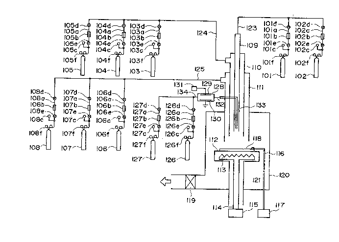
Fig. 1 shows an example of a preferable device
for practicing the method for forming a deposited film
of the present invention.
The deposited film forming device shown in Fig.
1 is broadly classified into the four of a main device,
an evacuation system, a gas feeding system, and an
activation chamber.
In the main device, a reaction space and a
film forming space are provided.
101-108, 126, and 127 are respectively bombs
filled with the gases to be used for film formation,
93162
- 24 -
1 lOla-108a, 126a, and 127a are respectively gas feeding
pipes, lOlb-108b, 126b, and 127b are respectively
mass flow controllers for controlling the flow rates
of the gases from the respective bombs, lOlc-108c,
126c, and 127c are respectively gas pressure gauges,
lOld-108d, 126d, 127d, lOle-108e, 126e, and 127e are
respectively valves, and lOlf-108f, 126f, and 127f
are respectively pressure gauges indicating the
pressures in the corresponding gas bombs.
128 is an activation chamber, 129 and 130 are
electrodes, 131 is a high frequence power source, 132
an activated species feeding pipeline, and 133 an
activated species introducing pipe.
120 is a vacuum chamber equipped at the upper
lS portion with a pipeline for gas introduction, having
a structure for formation of the reaction space
downstream of the pipeline, and also having a structure
for formation of a film forming space in which a
substrate holder 112 is provided so that a substrate
11~ may be provided as opposed to the gas discharging
outlet of said pipeline. The ~ipeline for gas
introduction has a quadruple concentric arrangement
structure, having from the innerside a first gas
introducing pipe 109 for introducing the gases from
the gas bombs 101 and 102, a second gas introducing
pipe 110 for introducing the gases from the gas bombs
103-105, a third gas introducing pipe 111 for
33~L6Z
- 25 -
1 introducing the gases from the gas bombs 106-108, and
an introducing pipe 133 for introducing the activated
species activated in the activation chamber 128.
For gas discharging to the reaction space of
each gas introducing pipe, each position is designed
so as to be arranged at a position further from the
surface position of the substrate as the pipe is nearer
to the inner side. In other words, the gas introducing
pipes are arranged so that the pipe on the outer side
may enclose the pipe existing within the innerside
thereof.
The gases from the respective bombs are fed
into the respective introducing pipes through the gas
feeding pipelines 123~125, respectively. The activated
species 5BA) are fed through the activated species
- feeding pipeline 132 into the activated specles
introducing pipe 133.
The respective gas in~roducing pipes, the
respective gas feeding pipe lines, and the vacuum
chamber 120 are evacuated to vacuum through the main
vacuum valve 119 by means of a vacuum evacuating device
not shown.
The substrate 118 is set at a suitable desired
distance from the positions of the respective gas
introducing pipes.by moving vertically the substrate
holder 112.
In the case of the present i.nvention, the
3.;2~
~62
- ~6 -
1 distance between the substrate and the gas discharging
outlet of the gas introducing pipe may be determined
appropriately in view of the kinds and the desired
characteristics of the deposited Eilm formed, the gas
flow rates, the inner pressure in the vacuum chamber,
etc. It is preferably several mm to 20 cm, more
preferably 5 mm to about 15 cm.
113 is a heater for heating the substrate which
is provided in order to heat the substrate to an
appropriate temperature during film formation, to
preheat the substrate 118 before film formation, or
further to anneal the film after film formation.
The substrate heating heater 113 is supplied
with power through a conductive wire 114 from a power
lS source 115.
116 is a thermocouple for measuring the
substrate temperature (Ts) and is electrically connected
to the temperature display device 117.
The present invention described in more detail
by referring to the following Examples.
Example 1
By use of the film forming device shown in Fig.
1, an electrophotographic photosensitive member shown
in Fig. 4 was prepared according to the method for
forming deposited film of the present invention.
The above photosensitive member for electro-
photography (Fig. 4) was constituted of an aluminum
62
- 27 -
I substrat~ 400, a charge injection impeding layer
~first layer p type, A-Si:H layer, 5 ~m) 401, a
photosensitive layer (second layer, non-doped A-Si:H
layer, 18 ~m) 402, and a surface protective layer
(third layer, ~-SiCH layer, 0.5 ~m) 403.
The preparation procedure of the photosensitive
member for electrophotography prepared under the
conditions in Table 1 of this Example is to be described
in detail with reference to Fig. 1.
An aluminum substrate 118 was placed in the
vacuum chamber 120, and heated to 280C by the heater
113 for heating the substrate. After the aluminum
substrate temperature became constantly 280C, silane
gas was introduced from the silane gas bomb 101 at
10 sccm, a gas mixture of helium and fluorine from the
fluorine gas bomb 103 diluted to 10% with helium at
100 sccm through the introducing pipes 123 and 124
into the vacuum chamber 120, and also a gas mixture of
diborane and helium from the gas bomb 106 of diborane
diluted with helium to 1000 ppm through the introducing
pipe 111 at 0.8 sccm into the vacuum chamber 120.
Further, nitrogen monoxide gas from the nitrogen
monoxide bomb 126 was introduced into the activation
chamber 128 at 0.8 sccm, and nitrogen monoxide was
activated by the power S0 W from the high frequency
power source 131 in the activation chamber, followed
by introduction of the activated species through the
~93~
- 28 -
1 introducing pipe 133 into the vacuum chamber 120.
Through the chemical reaction among the gases
thus introduced into the vacuum chamber, a first layer
was deposited to 5 ~m on the aluminum substrate 118.
After deposition of the first layer to 5 ~m,
feeding of diborane and nitrogen monoxide were stopped,
and sila~e gas and fluorine gas diluted with helium
were introduced at the respective flow rates of 40
sccm and 400 sccm to form a second layer to 18 ~m
through the chemical reaction of the introduced gases.
Then, the flow rate of silane gas was changed to 1
sccm and that fluorine gas diluted with helium to 10
sccm, and further methane gas from the methane gas
bomb 127 was introduced into the activation chamber
128 at 100 sccm, wherein methane gas was activated at
a high frequency power of 50 W, followed by introduc-
tion of the activated species into the vacuum chamber
120.
Through the chemical reaction among the gases
thus introduced, a third layer was deposited to 0.5 ~m.
The film thickness of each sample was
determined with a layer thickness measuring apparatus
of alpha~step ~produced by TENCOR Co.).
When the electrophotographic characteristics
of the photosensitive member for electrophotography
were measured, it was found that charg.ing ability was
improved by 30~ and the sensitivity by 10~, as compared
3~Eii2
- 29 -
I with that of the prior art.
Example 2
In the deposited film forming device shown in
Fig. 1, the activation chamber 128 was exchanged with
an activation device utilizing optical energy of
excimer laser shown in Fig. 2.
The activation device shown in Fig. 2 was
constituted of an activation chamber 201, an excimer
laser 202, a window 205 for irradiation of excimer
laser, and a gas feeding pipeline 203 connected to the
gas feeding pipeline 134 in Fig. 1, and also a gas
feeding line 204 connected ~o the gas feeding pipeline
132 in Fig. 1.
By utilizing the deposited film forming device
having the acti~ation device utilizing optical energy
as described above, a solar battery as shown in Fig. 5
was prepared according to the method for forming
deposited film of the present invention.
The above solar battery was constituted of 7059
glass (produced by Corning Co.) 500 having transparent
electrodes vapor deposited thereon, a p-type amorphous
silicon layer (first layer thickness 200 ~) 501, a
non-doped amorphous silicon layer tsecond layer,
thickness 7000 A) 502, an n-type amorphous silicon
layer (third layer~ thickness 200 A) 503, and an aluminum
electrode 504.
During formation of the deposited films, the
3~L~2
- 30 -
1 methane gas bomb in Example l was changed to an
ethylene gas bomb and also the nitrogen monoxide
bomb to a diborane bomb diluted to lO0 ppm with helium
to form deposited films.
Ethylene and diborane were mixed with each
other and introduced into an activation chamber
utilizing optical energy to be activated therein, and
then introduced into the vacuum chamber 120. Following
otherwise the same procedure as in Example l under the
conditions shown in Table 2, deposited films were
' formed.
The film thickness of each sample was deter-
mined in the same manner as in Example l.
The solar battery thus obtained exhibited a
conversion efficiency improved by lO~ as compared with
the solar ba~tery of the prior art.
Example 3
In the deposited film forming device in Fig. l,
the activation chamber 128 was exchanged with an
aotivation device having an electric furnace shown in
Fig. 3.
The activation device shown in Fig~ 3 was
constituted of an activation chamber 30l, an electric
furnace 302, a gas feeding line 303 connected to the
gas feeding pipeline 134 in Fig. l and a gas feeding
line 304 connected to the gas feeding pipeline 132 in
Fig. l.
~.~!93~
- 31 ~
1 By utilizing the deposited film forming device
having the activation chamber utilizing heat energy
as described above, a photosensitive member for
electrophotography was prepared under the conditions
in Table 3.
The film thickness of the first to the third
layer in said photosensitive member for electrophoto-
graphy were the same as in Example, and were measured
in the same way as in Example 1.
The photosensitive member of this Example was
pr~pared as follows. First, after the aluminum
substrate temperature was made constantly at 250C,
the first layer was formed by the chemical reaction
among the respective starting gases in Table 3
introduced into the vacuum chamber 120.
The second layer was formed by activating only
the germanium gas of the gases in Table 3 in the
electric furnace (700C) and introduc~d into the vacuum
chamber 120, with ~he other gases being directly
ln~roduced into the vacuum chamber 120, thereby
carrying out the chemical reaction among the gases.
The third layer was formed by the chemical
reaction among the respective starting gases in Table
3 introduced into the vacuum chamber 120.
The image forming member for electrophotography
prepared as described above was found to be improved in
sensitivity by 10% as compared with that of the prior art.
62
1 Example 4
By use of the film forming device shown in
Fig. 1, a thin ~ilm transistor (hereinafter called
"TFT") as shown in Fig. 6 was prepared according to
the method for formation of deposited film of the
present invention.
The above TFT was constituted of 7059 glass
~produced by Corning Co.) 634, an amorphous silicon
layer (first layer thickness 7000 A) 633, an amorphous
silicon layer doped with phosphorus to a high
concentration (second layer thickness 500 A) 632, a
silicon oxide layer (third layer thickness 1000 A~ 631,
and an aluminum electrode 629.
The film thickness of each sample was
determined in the same manner as in Example 1.
In this Example, on deposition of the amorphous
silicon layer doped with phosphorus to a high
concentration, in the activation chamber 128 shown in
Fig. 1, after the valence electron controller PH3 was
a~tivated by RF glow discharge, the activated species
formed from PH3 was introduced into the deposition
chamber 120 through the introducing pipe 133 to
deposite an amorphous silicon layer doped with
phosphorus to a high concentration. As to other
conditions, semiconductor layers and insulating layers
necessary for TFT were prepared under the conditions
shown in Table 1.
62
1 The TFT of the present Example exhibited an
on-off ratio improved by lO~ as compared with that of
the prior art.
As can be seen from the detailed description
and the respective examples as set forth above,
according to the deposited film forming method of the
present in~ention, deposited films havin~ uniform
physical characteristics over a large area can be
obtained with easy management of film quality at the
same time as achievement of energy saving. Also, it
is possible to obtain easily films excellent in
productivity, ~ulk productivity, having high quality
with excellent physical properties such as electrical,
optical, and semiconductor properties, etc.
Example 5
Films were formed on glass plates 7059
(produced by Corning Co.) for measuring the optical
band gas (Eg opt) under the same conditions as the film
fornnation conditions for the corresponding layer
de~cribed in Tables 1-4 to prepare sa~nples for
measuring Eg opt.
Each sample was subjected to spectrophotometric
determination with a spectrophotometer (produced by
HITACHI-SEISAKUSHO No. 330). Eg opt was calculated
from the results by the usual TAUC plot method.
The reference was prepared under the same
conditions as those in the second layer of Table l.
o~
- 3~ -
I Table 5 shows the results. As can be seen from Table
5, it has been found that each sample has an Eg opt
adjusted according to the object.
Table 5
Sample No. Corresponding layer in Table Eg opt ~eV)
1 First layer in Table 1 1.85
2 Third layer in Table 1 2.4
3 First layer in Table 2 2.0
4 Second layer in Table 3 1.5
Third layer in Table 4 2.0
Reference Second layer in Table 1 1.7
~ ~93~L62
-- 35 --
~ a
lo
,1 ~ r~ 3 ~ 3
~, ~ ~0
. Zj~
_
~ a) e .
~ o ~ o O C~ ~ O O O ~ O O
15 E~ ~"~u ~ ~ ~ o ~ ~
. ~ e .
0~ .
0_~ ,i O
20 ~ ,~: ~ 11 11
S-l ~r X ~C~D 5~ ~ ~ r
~ .,1 ~ ~ O .,~ ~ .,1 ~ 5
~q u~ q z u~ ~ ~n ~4 u
. .
1 ~: ~d
h ~ O ~ h ~ h ~ h
a) u~ tQ O~ O a~ ~ a
~ O ::~ h ~ U
~ 1~ ~ 1 E~
3.~93~2
5 ~ ~P~ ~ ~
1~ ~ l i~
. ~-I.C X ~ ~1
. ~ ~ .,~
~ ~ .
~ ~ O
t~ C~ rd O
...__ .
o o o o
,~:1 ~1 ~1 U ~ O ~ 1
15 E~ ~ h ~n __
~a~
. .~ o ~'
, o o o o o
. ~ ~ 11 ~1
- .~:: ll m ll n ~
m
h ~ m ~ ~ ~ m ~ m
~ ~ C 5: ~
.~ .,, ~ ." ~ m
u~ u~ ~m c~ ~n E4 u~
h ~ O ~ h ~ h ~ h
~, ~ o a) ,~1
~ o ~ ~1 ~ a) ~ ~ ~
~ o ~ ~ ,~ _ ____
~ ~93~.~2
5 ,t~P ~ o
10 ~ ~ I U "
~.,, .
~_i 3 ~ ~ o o ~ o o ~ o ~ o o
R ~1 0 o ~1 o ~ o ~1 o
15 E~ ~ ~1 ~ .
. h o o o o
~ ,1 ~ ~
20 ' ~: ~ D '~ ~ :~
~ ~ .~ O .~ .~
_ r~Z U~ ~
h O t) ~ ~ S~
25 O~
93162
-- 38 --
3 ~, El o o I o c N I
E~ _ N O ~1 O ~1 ~1 _1 .
' E ~ ~1 o ~1
~.0 ~ ~1 ~: ~.1 `25 ~1
25 ~ ~ ~ U~ ~