Note : Les descriptions sont présentées dans la langue officielle dans laquelle elles ont été soumises.
(~IRCUIT BOARD PIN
This inventlon relates to circuit board pins.
Circuit board pins are constructed for two basic
methods of mounting into conductively lined pin receiving
5 holes in printed circuit boards. In one of these methods,
the pins are held within the holes by use of solder. By
the other method, the pins are constructed to have
compliant portions which are resiliently flexible. With
these pins, the compliant portions are located in the
lo holes, which are smaller in diameter than a critical
dimension across the compliant portions, thereby
resiliently moving parts of the compliant portions
laterally of the pin to reduce this critical dimension and
hold surfaces of the compliant portions gastightly in
contact with the conductive lining of the holes.
Compliant portions of pins may be constructed
according to one of many basic designs. In one of these
designs sometimes referred to as the "eye of the needle'l,
the compliant portion has two beams extending side-by-side
axially of the pin and spaced apart by a slot extending
through the pin. The beams merge together at each end o~
the compliant portion and also into other pin portions
extending from the ends of the compliant portion. The ~eye
of the needle" design is considered ideaI because is it
sy~netrical about the pin axis and doesnlt tend to cause
pin rotation as it is inserted into a hole in a printed
circuit board. In addition, the beams move resiliently
towards each other during pin insertion without any
tendency to create pin asymmetry which would cause tilting
of the pin.
- However, the "eye of the needle~' compliant portion
has the disadvantage that it has a smaller area of contact
with a conductive lining of a printed circuit board hole
than does a compliant portion of some other designs. This
provides for a smaller positive conductive path from the
pin to the printed circuit board with the "eye OL the
needlell design. Also, the smaller contact area provides a
3~3
smaller distribution of the load from the resilient beams
into the conductive lining of the holes. This results in
high localized pressure which may result in cutting into
the lining thereby producing deterioration of the circuit
board and a weakened conductive path.
The present invention provides a circuit board pin
having an "eye of the needle" compliant portion and a
method and apparatus for producing such a pin and which
seeks to alleviate the above problems.
lo According to one aspect of the present invention
there is provided a circuit board pin comprising a
compliant portion extending for a part of the length of the
pin, and other portions, one at each end of the compliant
portion, the compliant portion comprising two resiliently
flexible beams which extend along the compliant portion in
spaced side-by-side relationship, one on each side of a
slot extending longitudinally of the pin, the beams having
oppositely outwardly facing surfaces which are convex in
lateral cross-section of the beams and, in side elevational
view and in plan view of the pin:- a) the convex outwardly
facing surfaces extend outwardly beyond boundaries of the
other portions; and b) the compliant portion tapers down
into the other portions to effect merging of the beams
together and with the other portions beyond ends of the
slot.
As can be seen from the circuit board pin of the
invention, the outwardly facing surfaces of the beams
extend not only outwardly from other portions of the pin in
plan view but also extend outwardly in side elevation. As
a result, these convex surfaces are wider than would be the
case if they merely extended beyond other portions of the
pin in plan view alone. The convex surfaces thereby
provide a wider surface and hence a greater surface area
for conductively contacting the lining material of a hole
in a circuit board. The greater surface area for contact
reduces the unit pressure on the hole surface with an
3;~3
attendant reduction in the chances of cutting through the
lining material.
According to another aspect of the present
invention there is provided a method of making a circuit
board pin having a compliant portion between two end
portions comprising:- providing a length of non-tubular
material for the pin; making a preform for the compliant
portion of the pin by forming a slot through the length of
material, the slot extending longitudinally of the length
lo and spaced from ends of the length to provide an end
portion of the pin at each end of the slot and two beams of
the compliant portion, the beams extending outwardly from
each side of the slot beyond the end portions along the
complete length of each beam; applying a beam deforming
pressure against outer lateral edges of the beams to urge
the beams inwardly towards each other to decrease the width
across the beams and to narrow the slot until the beams
engage a pressure resisting surface disposed within the
slot; and completing the compliant portion by continulng to
apply the beam deforming pressure inwardly towards the
slot:- a) to compress the beams against the pressure
resisting surface and reduce the lateral width of each beam
while simultaneously expanding the beams outwardly at each
side in directions parallel to the depth direction of the
slot wherein the depth direction is the direction from one
opening of the slot to the other; and b) to deform the
outer lateral edges of the beams into convexly curved
shapes when considered at any cross-section along the beams
normal to the longitudinal direction of the pin, said
convexly curved lateral edge of each beam, at any such
cross-section, lying outwardly beyond boundaries of the end
portions both in directions normal to and directions
parallel to the depth direction of the slot.
AS can be seen from the above method of the
invention, in the preform the edges of the beams extend
beyond the width dimension of the two end portions before
completion of the compliant portion. During completion of
`' ~i'~ .
the compliant portion, the beams are deformed in the
thickness dimension so as to extend outwardly also beyond
the two end portions in the thickness direction also. The
width of the convex curved surfaces is thus greater than
would be the case without this type of deformation.
In a preferred method of making the invention, the
pin is formed from a length of wire have oppositely facing
surfaces which firstly provide the outer lateral edges and
then the convexly curved surfaces of the beams. In this
preferred method, drawn wire has substantially smooth
surfaces and these smooth surfaces need to be coined or
deformed solely for the purpose of forming the convexly
curved surfaces and not for providing any substantial
improvement of the smooth surface finish. On the other
hand, it is within the scope of the invention to form the
pin from sheet material by providing a pin blank which
involves blanking material from either side of the blank.
with such a method, however, the outer lateral edges of the
beams so formed would not have the smoothness of the drawn
wire and greater difficulty would be found in producing the
smooth convexly curved surfaces in the completed compliant
portion.
It is preferable also that in the method the wire
is of rectangular cross-section. Such wire would have a
2s width dimension bounded by a first pair of oppositely
facing surfaces and a thickness dimension bounded by a
second pair of oppositely facing surfaces. The width of
the wire is reduced by removal of the wire material at each
of the first pair of surfaces in axially spaced regions of
the wire to form the two end portions of the pin. A slot
is formed in a region intermediate the two end portions to
form the preform in the intermediate region with the first
pair of oppositely facing surfaces providing the outer
lateral edges. The beam deforming pressure is then applied
inwardly against the outer lateral edges of the beams to
deform them outwardly in opposite directions in the
direction of the thickness dimension beyond each surface of
33~
the second pair. This causes the convexly curved surfaces
to extend bo~h beyond the reduced width dimension and the
thickness dimension of the two end portions.
The method also preferably includes forming the
slot to a width greater than that finally required and
reducing the width during the application of the beam
deforming pressure to the desi.red slot width. With this
process step, the slot of greater width is more easily
blanked from the wire and the application of the beam
lo deforming pressure enables the slot to be reduced to that
desired, such as would be obtained with good manufacturing
practice, e.g. the width of final slot to thickness of wire
ratio of around l:1 or even less.
The invention further provides an apparatus for
making a circuit board pin including means for forming a
compliant portion of the pin from a preform having two
beams extending axially of the pin and, in plan view of the
pin, side-by-side and spaced apart by an axially extending
slot, the co~pliant pin forming means defining a pin
location station and comprising:- pressure applying
elements spaced-apart in a plane across the station and
oppositely acting to move towards each other to inner
positions and to move apart from said inner positions in
said plane, the pressure applying elements having opposing
surfaces for forming oppositely outwardly facing surfaces
of the beams, which surfaces are convex in lateral cross-
section; at least one pressure resisting member which is
movable normal to the plane to an inner position across the
pin location station for location within the slot before
movement of the pressure applying elements towards each
other so as to control the width of the slot during
application of pressure to the beams; the pressure
resisting member and the pressure applying elements in
their inner positions together defining two beam shaping
cavities with the concave surfaces providing cavity
defining surfaces; and holding means for holding a length
~3~3
of material for forming the pin in the pin location
stati.on.
One embodiment of the invention will now be
described by way of example, with reference to the
accompanying drawings, in which:-
Figure 1 is a plan view of a prior art circuitboard pin to a much enlarged scale;
Figure 2 is a cross-sectional view taken along line
II-II of the prior art pin of Figure l;
Figure 3 is a cross-sectional view through a
printed circuit board showing the prior art pin of Figure 1
assembled into the board by reception of a compliant
portion of the pin within a hole of the board;
Figure 4 is a cross-sectional view taken along line
15 IV-IV of the assembly in Figure 3 and to a smaller scale;
Figure 5 is a view, similar to Figure 1, of a
circuit board pin according to the embodiment to a much
enlarged scale;
Figure 6 is a cross-sectional view taken along line
VI-VI in Figure 5;
Figure 7 is a side elevational view of the pin of
the first embodiment taken in the direction of arrow VII in
Figure 5;
Figure 8 is a cross-sectional view through a
compliant portion of the pin of the embodiment showing the
pin assembled into a hole in a circuit board;
Figure 9 is a plan view of the pin of the
embodiment at one stage in its manufacture, and to a
smaller scale than Figures 5 to 8;
~o Figure 10 is a cross-sectional view through the
partially completed pin taken along line X-X in Figure 9;
Figure 11, to the scale of Figures 5 to 8, is a
cross-sectional view through an apparatus for forming the
: completed compliant portion of the pin, showing the parts
3S of the apparatus in an open position with a partially
formed pin inserted into a location station;
33~
Figure 12 is a cross-sectional view through the
apparatus taken along line XII-XII in Figure 11; and
Figures 13 and 14 are sections similar to Figure 11
and showing different stages in the operation of the
apparatus.
Figures 1 and 2 show a prior art circuit board pin
10 having a compliant portion 12. The compliant portion is
of the "eye of the needle'~ deslgn in that it has two side-
by-side beams 14 extending axially of the pin, the beams
being spaced apart by an axially extending slot 16. As
shown by Figure 1, in plan view, the beams extend laterally
beyond other portions 18 and 20 of the pin which extend
from the two ends o~ the compliant portion 12. As shown by
Figure 2, the pin is of constant thickness from end-to-end
whereby the compliant portion, i.e. the beams 14, are no
thicker than the other pin portions 18 and 20. Outer edges
22 of the two beams are convexly curved from end-to-end of
the beams to provide an area of contact with lining
material of a circuit board hole into which the pin is to
be inserted.
The prior art pin is assembled into a pin receiving
hole 24 of a printed circuit board 26, as shown in Figures
3 and 4. The end 18 of the pin is inserted through the
hole followed by the compliant portion 12. The distance
across the edges 22 is slightly greater than the diameter
of the hole whereby the hole resiliently flexes the beams
inward towards each other, in known manner, thereby
narrowing the slot 16 so that in the final position shown
in Figures 3 and 4, the compliant section is resiliently
held within the hole with the edges 22 resiliently pressing
against the inside surface of the conductive lining
material 28 of the hole.
As can be seen from Figure 3, the contact surface
area between the pin and the lining material 28 of the
printed circuit board is small compared to the total inner
surface of the lining ma~erial. Apart from minimizing the
circuit path between the pin and the lining material, the
~3~3
pressure applied by the small area of contact may result in
cutting into the lining material to cause deterioration of
the lining material and a reduction in the effectiveness of
the circuit path. Further to this, in the construction of
s the prior art pin, the width of the slot 16 is preferably
made according to good machinery practice in a ratio of
approximately l:l in relation to the thickness of the
material of the pin. However, the slot 16 needs to be
blanked from the material and the blanking of a slot with
lo such a width to material ratio may be technically
difficult.
The present invention provides a circuit board pin
and a method of producing such a pin which alleviates the
above disadvantages. This is clear from the embodiment now
to be described.
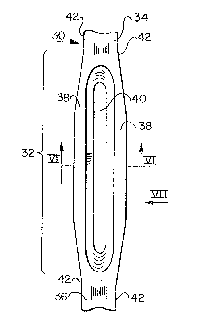
As shown by Figure 5, a circuit board pin 30
according to the embodiment comprises a compliant portion
32 extending axially of the pin and other portions 34 and
36 of the pin extending axially from the two ends of the
compliant portion.
AS in the prior art construction discussed above,
the compliant portion 32 is of the "eye of the needle" type
of construction and has two side-by-side beams 38 which
extend axially of the pin and are spaced apart by a
longitudinally extending slot 40 over the compliant
portion. The portions 34 and 36 of the pin are of
rectangular or s~uare cross-section and have edge surfaces
42 ~Figures 5 and 6) beyond which the beams 38 extend. In
this respect the pin 30 is also similar to the pin 10 of
the prior art.
The pin 30 differs however from the prior art pin
in the manner shown in Figures 6 and 7. AS shown in
Figures 6 and 7 the two beams 38 not only extend outwardly
beyond the surfaces 42, but also extend outwardly beyond
the other surfaces 44 of the rectangular pin portions 34
and 36. The beams 38 have oppositely outwardly facing
surfaces 46 which are convex in lateral cross-section of
,7
3~3
the beams as shown in Figure 6. These surfaces extend
outwardly beyond the surfaces 42 because the beams extend
beyond these surfaces as has been described. ~lowever, in
addition, because the beams 38 extend outwardly beyond the
surfaces 44 also, then the surfaces 46 have a lateral width
(as shown in Figure 6) which is greater than the distance
between the surfaces 44. Surfaces 46 extend beyond
surfaces 44 to positions 48 which approximately lie at the
remote positions of the beams. In other words, the
lo surfaces 46, both in plan view (Figure 5) and side
elevational view (Figure 7), extend outwardly beyond the
boundaries of the pin portions 34 and 36, these boundaries
being the surfaces 42 and 44. Also, because of the
geometry of the structure, the compliant portion tapers
down into the portions 34 and 36 to effect a merging
together of the beams and also into the other portions
beyond the ends of the slot 40. This tapering action
occurs both in the plan view of Figure 5 and the side
elevational view of Figure 7. It will be clear that the
pin 30 provides a greater surface area (i.e. surfaces 46)
for electrical contact with lining material in a pin
receiving hole of a circuit board, than is possible with
the surface area of the prior art pin.
The pin 30 is fitted into a pin receiving hole 51
of a printed circuit board 50 (Figure 8) in the manner of
insertion described with regard to the pin 10. The pin 30
is held in position by reception of its compliant portion
32 within the layer 52 of conductive material forming the
hole of the printed circuit board. With the surfaces 46
having the correct characteristic of curvature to suit the
inner diameter of the insulation, it will be appreciated
that a substantial arc 54 of contact occurs between each
surface 46 and the conductive layer 52 and that this arc of
contact far exceeds anything possible between the prior art
pin 10 and the conductive lining material of its associated
hole. In fact, as can be seen from Figure 8, the arc 54 of
contact between the two surfaces extends substantially
beyond the surfaces 44 of the portions 34 and 36 of the
pln. The larger arc of contact between the two surfaces
proportionally increases the area of conductive contact
between the beams and the lining material.
In addition, the substantially wide convex surfaces
46 provide a further function. As the contact area between
surfaces 46 and the conductive layer 52 is substantially
large compared to prior art arrangements, then there is a
resultant decrease in pressure applied to the lining
lo material by the resilient flexing of the beams 38 although
the resilient outward load may be comparable to that in the
prior art beams. The reduction in pressure reduces any
tendency for the beams to cut into the insulation layer 52
whereby the tendency for deterioration of the printed
circuit board and for reduction in the conductive path is
minimized in the embodiment. It follows that in use of the
circuit board pin according to the embodiment and as
defined according to the invention, an improved circuit
path is provided into a printed circuit board with reduced
possibilities of damage resulting to the board or in a
reduction in the electrical performance of the assembly.
The pin 30 is made by the method and apparatus
described with reference to Figure 9 onwards.
The pin 30 is formed as one of a succession of pins
from a rectangular cross-section wire 56 shown chain-dotted
in Figure 9. The wire is drawn wire having substantially
perfectly smooth side edges 58 across a width dimension of
the wire, and top and bottom surfaces 44 across a thickness
dimension of the wire, (Figure 10), the surfaces 44
corresponding to the surfaces 44 of a finished pin.
A pin preform 60 is formed at the leading end of
the wire and is removed from the wire before formation of a
subsequent pin preform. Each pin preform is provided, in a
conventional manner for forming pin preforms from drawn
wire, by reducing the width of the wire in two axially
spaced regions 62 and 64 which are separated by an
intermediate region 65 which is to become a preform for the
~J~
3~3
11
compliant portion. The width of the wire is reduced by
removal of the wire material from each surface 57 in a
symmetrlcal fashion whereby the final cross-sectional shape
and size of the pin portions 34 and 36 are produced upon
s the pin preform. The intermediate region 65 progressively
tapers into the pin regions 34 and 36 as shown by Figure 9.
In addition, a slot 16a is provided extending
longitudinally of the intermediate region 65, and this
defines two rectangularly shaped beams 38a havlng outer
o lateral edges 58. The ratio of the width of the slot 16a
to the thickness of the wire or depth of the slot, i.e.
between surfaces 44, is substantially greater than l:1 as
this width of slot is easier to blank out.
The wire is then fed forwardly to locate the pin
preform 60 in a pin location station within apparatus which
includes means for forming the completed compliant portion
of the pin. As shown by Figures 11 and 12, the
intermediate region 65 is located between two pressure
applying elements 66 which are movable towards each other
and apart horizontally, between guides 68, towards and away
from the pin location station. The elements 66 have
concave opposing surfaces 70 for forming the oppositely
outwardly facing convex surfaces 46 on the beams. In
addition, the apparatus includes two pressure resisting
2s members 72 which are movable towards each other and apart
in a vertical plane and partly across the pin location
station. As can be seen from Figure 11, the two pressure
resisting me~bers 72 are also guided between the guides 68
and have reduced width ends 74 for location within the hole
16a as will be described. The reduced ends merge into
greater width parts of the members 72 by inclined surfaces
76. The elements 66 and members 72 are movable between
positions apart shown in Figure 11 and inner or positions
closer together as shown in Figures 13 and 14. In the
inner positions shown in Figure 14, the concave surfaces 70
and the side and inclined surfaces of ends 74 of members 72
define two cavities 78 for shaping the beams 38 and for
~33a~3
producing the taper into pin portions 34 and 36. In
addition, the apparatus is provided with means for holding
the length of material, i.e. the drawn wire, during
deformation of the preform 60 to make the compliant
portion. In this embodiment, the holding means comprises
vertically movable clamping members 80, which are moved to
inner clamping positions (as shown in Figure 12) before
movement of members 72 into their inner positions. These
clamping members 80 have clamping surfaces 82 for
lo engagement with the surfaces 44 of the pin portions 34 and
36.
In use of the apparatus shown in Figure 11 onwards,
the pin blank 60 is located in its pin location station
with the intermediate region 65 disposed between the
outwardly positioned elements 66 and members 72. The
clamping members 80 and the pressure resisting members 72
are then moved to their inner positions in which the
clamping members clamp against the surfaces 44 of the pin
regions 34 and 36 and the members 72 enter into the slot
16a until they abut each other as shown by Figure 13. In
this position, the inclined surfaces 76 of the members 72
also lie partly within the slots 16a. The elements 66 are
then moved inwardly from the position in Figure 13 to that
of Figure 14. During this movement the surfaces 70 engage
the outer lateral edges 58 of the beams 38a and
progressively coin them so as to provide the convex
surfaces 46 and also to displace the material in the beams
38a laterally into parts of the cavity 78. In this way,
the material in the beams 38a becomes displaced beyond the
surfaces 44, as shown in the finished structure of Figure
6. Hence the surfaces 46 are formed with their lateral
width sreater than the original thickness of the wire
itself. During the deformation process also, the material
of the beams 38a is displaced inwardly against the reduced
ends 74 of the members 72 so as to reduce the width of the
slot 16a to a desired width to thickness of material ratio,
e.g. around 1:1. This ratio has thus been produced while
3(~3
avoiding the usual difficult blanking operation to produce
such a ratio of slot width to material thickness.
As the starting material for the pin was drawn wire
then the edges 58 were particularly smoot~ at the beginning
of the coining operation so that coining is only required
to reshape the surfaces to form the surfaces 46 and opera-
tions are not required substantially to enhance smoothness
of the surface. The coining operation merely retains the
smoothness of the surface during deformation. In addition,
lo the coining operation provides some lateral grain flow in
the material of the beams thereby increasing their strength
beyond that provided by the grain flow extending axially of
the pin and inherent from the drawn wire.
After the compliant portion of the pin has been
formed, the pin together with other pins may be assembled
in spaced side-by-side relationship, i.e. in the form of a
conventional llbandolier'l, for any further operatlons upon
the pins to finish the end portions 34 and 36.
. . .~i,~ .