Note : Les descriptions sont présentées dans la langue officielle dans laquelle elles ont été soumises.
3i~
COMPLIANT PIN HAVING IMPROVED ADAPTABILITY
This invention relates to contact pins of the type
which are intended for insertion into circuit board holes
and which have compliant portions that are deformed when
inserted into the circuit board hole and which establish
electrical contact with conductive surface portions of the
hole.
Compliant pins are now being used in vast numbers in
the electronics industry when it is necessary to establish
contact with the conductors in a multi-layer board, a back
panel, or a simple circuit board having a plated through
hole. A aompliant contact pin has a compliant portion
which has a normal width which is greater than the hole
diameter but which can be deformed when it moves into the
circuit board hole so that contact edge portions of the
compliant portion will establish the electrical contact
required with the conductors in the circuit board hole.
The compliant portion thus is essentially a relatively
stiff spring system which, after insertion into the
circuit board hole, will bear against the surfaces of the
hole with sufficient force to retain the pin in the
circult board and to establish a sound electrical contact
with the circuit board conductors. Some commonly known
types of compliant pins are shown, for example, in U. S.
Patents 4,186,982, 4,743,081, 4,206,964, and 4,606,589.
Notwithstanding the fact that compliant pins are
presently being used in large numbers, there are many
circumstances under which it would be desirable to employ
compliant pin technology but in which it is not now
feasible to do so for the reason that most of the
presently known types of compliant pins lack adaptability
in the sense that the compliant pin must be manufactured
~rom metal stock having some minimum thickness and the pin
will not perform adequately if an attempt is made to
manufacture the pin from a stock metal which is thinner
than the required minimum. For example, a widely used
standard ~ized hole for circuit boards or other panel-like
members in which contact pins are mounted is 0.040 inches
(1.02 mm). Many of the presently available compliant pins
are manufactured from metal stock having a thickness of
0.025 inches (0.63 mm) if the pin is intended for
insertion into a 0.040 inch diameter hole. Some presently
available compliant pins can be produced from metal stock
having a thickness of 0.015 inches (0.38 mm) but with some
sacrifice o~ performance. Presently available contact
pins thus have only limited adaptability insofar as the
hole diameter and stock thickness relationships are
concerned.
There are many circumstances where a contact pin must
be inserted into a 0.040 inch (1.02 mm) diameter hole but
where it is impossible to use 0.025 inch thick stock or
14218 -2-
~L2938~'3
even 0.015 inch (0.~8 mm) stock ~or the pin~
Manufacturing cost considerations alone may limit the
thickness of the stock to 0.012 inches (0.30 mm) or less.
The stock thickness for a contact pin ~may also ~e limited
if the contact pin is integral with a ~spring receptacle or
the like which must, for mechanical reasons, be
manufactured from relatively thin stock metal. Circuit
board switches such as DIP switches, for example, contain
spring contacts which must be manu~actured from extremely
thin stock metal, say 0.008 inches (0.20 mm). It would be
desirable if the pin portion of the spring contacts could
be provided with a compliant portion so that the DIP
switch could be mounted on the circuit board by merely
inserting the contact pins which extend from the switch
housing into circuit board holes. At present, if the
circuit board hole size is the standard 0~040 inches as
noted above, and if the spring contact is of relatively
thin material, the connector or switch must be connected
to the circuit board conductors by conventional soldering
methods with a signi~icant increase in assembly cost over
comparable compliant pin assembly methods.
Some reduction in the stock thickness o a compliant
pin might be obtained if special manufacturing techniques
such as coining are resorted to, but such techniques would
increase manufacturing cost. The preferred method of
14218 -3-
.
3~23
manufacturing compliant pins is by simple stamping and
forming methods.
The present invention is directed to the achievement
of an improved compliant pin which has a wide range of
adaptability in the sense that the pin can be manufactured
from metal stock having a wide thickness range. The
invention is al50 directed to the achievement of a
compliant pin which can be manufactured by conventional
known stamping and forming methods and which does not
require highly critical and sensitive metal working steps
in its production.
The inventlon comprises a contact pin which is
intended ~o be inserted into a circuit board hole, the pin
having a compliant portion which is deformed upon
insertion and which establishes contact with conductive
surface portions of the hole after insertion. The contact
pin i8 characterized in that the compliant portion has a
lead-in portion, an intarmediate portion, and a trailing
end portion. The intermediate portion has a width which
is greater than the diameter of the circuit board hole and
the lead-in portion has a width which is less than the
diameter of the circuit board hole. The compliant portion
is of increasing width between the lead-in portion and the
intermediate portion. The compliant portion has a pair of
spaced-apart openings thereinj one of the openings being
proximate to the lead-in portion and the other opening
14218 -4-
, :
l2~3~23
being proximate to the trailing end portion. The
compliant portion is sheared along a shear line which
extends between the openings so that the openings and the
shear line divides the compliant port:ion into a pair of
side-by-side beams. Each beam has an intermediate
portion, one fixed end at the lead-in portion, and another
fixed end at the trai~ing end portion. Each beam has a
stop in the ~orm of an ear which extends from its
intermediate portion towards the other beam. The ears are
defined by the edges of the openings and the shear line.
The intermediate portions of the beams, including the
ears, are displaced by a forming operation in first
opposite ~irections normally of the longitudinal axis of
the pin and away from each other thus placing the ears in
spaced-apart planes. In use, and upon movement of the
compliant portion into the circuit board holej lead-in
portion first, the beams are moved towards each other in
second opposite directions. The second directions are
normal to the first directions and the ears are thereby
moved into overlapping relationship so that the ear of
each beam functions as a support or stop for the other
beam at a location intermediate the ends of the other
beam. Upon further movement of the compliant portion into
the circuit board hole, the beams are moved additional
distances in the second opposite directions and flexed,
the flexure of the beams giving rise to contact forces of
14218 -5-
93~23
67789-259
the beams with the conductive surface portions of the hole.
Advantageously, the contact pin as described above is a stamped
and formed pin having oppositely facing rolled surfaces and shear-
ed side edges and the openings in the compliant portion extend
through the rolled surfaces. The intermediate portions of the
beams may be in substantially parallel spaced-apart planes prior
to insertion of the pin into the circuit board hole or they may be
in opposed offset concave relationship.
According to another aspect of the invention, there is
provided a contact pin which is destined to be inserted into a
circuit board hole, the pin having a compliant portion which is
deformed upon inæertion and which contacts conductive surface
portions of the ~ole, the contact pin being characterized in that:
the compliant portion has a lead-in portion, an intermediate
portion, and a trailing end portion, the intermediat~ portion
having a width which is greater than the diameter of the circuit
board hole, the lead-in portion having a width which is less than
the diameter of the circuit board hole, the compliant portion
being of increasing width between the lead-in portion and the
intermediate portion, the compliant portion being severed along a
severing line which extends from the lead-in portion to the trail-
ing end portion, the severing line dividing the compliant portion
into a pair of side-by-side beams, each beam having an inter-
; mediate portion, one fixed end at the lead-in portion and another
fixed end at the trailing end portion, the intermediate portions
of the beams being displaced in first opposite directions normally
of the longitudinal axis of the pin, and at least one of the beams
-- 6 --
~2931323
67789-259
having a stop portion intermediate its ends, the stop portion of
the one beam being adjacent to the severing line and extending
towards the other beam whereby, upon movement of the compliant
portion into the circuit board hole, lead-in portion first, the
beams are moved towards each other in second opposite directions,
the second opposite directions being normal to the first opposite
directions, and the stop means of the one beam is thereby moved
into overlapping relationship with the other beam whereby the
beams support each other at locations intermediate the ends of the
beams, and upon further movement of the compliant portion into the
hole the beams are moved further distances in the second opposite
directions.
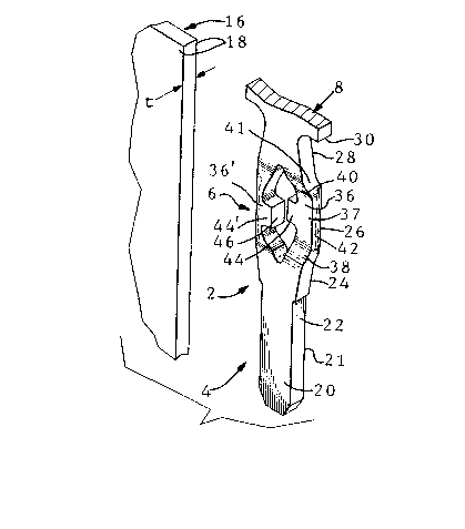
FIGURE 1 i8 a perspective view of a contact pin in
accordance with the invention and shows also a short section of
strip stock me-tal.
FIGURE 2 is a frontal view of the compliant portion of
the contact pin of Figure 1.
FIGURE 3 is a side view looking in the direction of the
arrows 3-3 of Figure 2.
FIGURES 4 and 5 are views looking in the direction of
the arrows 4-4 and 5-5 of Figures 2 and 3 respectively.
FIGURES 6, 7, 9, and 10 are views illustrating the move-
ment of the compliant portion into a circuit board hole and illu-
strating the manner in which the compliant portion is flexed dur-
ing such movement.
FIGURES 8 and 11 are views looking in the direction of
the arrows 8-8 a.nd 11-11 of Figures 7 and 10 respectively.
- 6a -
, . ;.,
1293~323
FIGURES 12-16 are views showing alternative compliant
portions of contact pins.
FIGURE 17 is a theoretical curve o~ the force and
insertion distance relationships of a contact compliant
pin in accordance with the invention.
FIGURE 18 is a cross-sectional vilew of one of th~
beams which forms part o~ the compliant portion of ~he
contact pin and is used for purposes of explanation.
Referring to Figures 1-5, a contact pin 2 in
accordance with the invention has a pilot portion 4, a
compliant portion 6, and an adjacent portion 8. The pin
is intended to be inserted into a hole 10 in a aircuit
board 12 which has metalized surface portions 14 so that
contact will be established with these metalized portions
by the compliant portion of the pin 2. The pilot portion
4 has a cross-section such that it will fit freely through
the hole and the compliant portion is deformed when it
enters the hole as will be described below.
The embodiment of the invention shown in Figures 1-5
is manufactur~d by stamping and forming sheet metal stock
16 which has oppositely facing rolled surfaces 18 and
which has a thickness t. The rolled surfaces 18 are so
called for the reason that they were contacted and
squeezed between the rolls when the stock metal was
formed. ~he rolled surfaces are also identified in the
14218 -7-
1~3~3
stamped and formed pin which has also sheared edge
surfaces as de~cribed below.
The pin 2 has oppositely facing rolled surfaces 20,
21 extending along its length and sheared edges as shown
at 22. The compliant portion 6 has a l,ead-in portion 24
which is adjacent to the pilot portion of tAe pin, an
intermediate portion 26, and a trailing end portion 28
which adjoins the adjacent portion 8 of the pin. The
adjacent portion has a downwardly facing shoulder 30 which
functions as a stop when the pin is inserted into the
circuit board and insures that the compliant portion wil}
be in the circuit board hole as shown in Figure 11.
Two punched triangular openings 32 are provided in
the compliant portion, and the compliant portion is
sheared along a shear line 34 which extends between these
openings. The shear line 34 lies on the longitudinal axis
of the pin. The openings are generally triangular and
have apices which are proximate to the lead-in portion and
the trailing end portion respectively and have bases which
intersect the shear line 34. The openings and the shear
line divide the compliant portion into two side-by-side
beams 36, 36' which are on each side of the longitudinal
axis the pin. Each beam has one fixed end 38, 38' at the
lead-in portion and another fixed end 40, 40' at khe
trailing end portion. Each beam also has an outwardly
facing sheared edge 41 which is chamfered in the
14218 -8-
~2~3~1~3
intermediate portion as shown at 42 so that these edyes
will conform to the cylindrical surface of the circuit
board hole lO.
The holes 32 and the shear line 34 de~ine a pair of
ears 44, 44' which extend from each beam int~rmediate its
ends toward the other beam. The ears have opposed ends 46
which are on the central axis of the pin and which are the
sheared surfaces resulting from the shearing of the pin
when the beams were produced.
The central, or intermediate, portions 37 of the
beams 36 are formed in first opposite directions away from
each other so that after forming, the intermediate
portions 3'7 of the baams and the ears 44, 44' are in
parallel spaced-apart planes as shown in Figure 3. The
portionR of the rolled surfaces 20, 21 on the ears ~4, 44'
are opposed to each other as shown in Figure 4 and the
ends 46 of the ears are coplanar. The manufacturing
process for producing the pin 2 is thus extremely simple
requiring only the blanking, hole punching, shearing of
the shear line 34, and the forming of the beams by bending
them in the opposite first directions.
When the pin is inserted into the circuit board hole
lO, it is aligned with the hole and the pilot portion 4 is
moved into the hole until the lead-in portion of the
compliant portion engages the upper edges o~ the hole.
Because o~ the fact that the central portions of the beams
1421~ -9-
~Z93~323
are offset, the corners 42, 42' will engage edge portions
of the hole at opposite locations. As insertion proceeds,
the beams will be moved diayonally towards each other and
into overlapping relationship as shown in Figure 7. That
i~, the beams will be moved in first reverse directions
which ar the reverse of the first opposite directions
back towards their original positions that they occupied
prior to forming. At the same time, the beams ~ill be
moved in second opposite directions which are normal to
the first opposite directions so that the beams move into
overlapping relationship as indicated by the dotted line
in Figure 7. The resultant movement is diagonal, as
explained above, of the beams towards each other.
After the ears overlap each other as shown in Figure
7 even by a slight amount, further movement of the beams
in the first reverse directions, that is back to their
original positions, is impeded or stopped entirely and
further flexure of the beams takes place in the second
opposite directions. In other words, the beams move
further into overlapping relationship as shown in Figure 9
and are flexed along their lengths during this stage o~
the insertion. When the beams are fully inserted, Figures
lO and ll, the contact surfaces 42 are urged against the
conductive surface portions of the circuit board hole 10
by stresses in the beams which result from the flexure of
1421~ -lO-
1293~323
the beams in the second opposite directions and the
flexure o* the beams in the first reverse directions.
The movement of the beams in the first reverse
directions as discussed above may be extremely slight and
may be insignificant as compared to th~s movement of the
beams in the second opposite directions. If a particular
pin is designed such that there is a gap between the
surfaces 20,21l there will be significant movement in the
first reverse directions but if there is no gap, the
movement in the first reverse directions will be
insignificant. In all cases, there must be sufficient
movement in the second opposite directions at the outset
o~ the insertion process to bring the ears into
overlapping relationship so that the ears will not be
returned to coplanarity by movement of the ears in the
first reverse directions.
An important feature of the invention is that whsn
the ears 44, 44' move into overlapping abutting
relationship as shown in Figures 7 and 8 and the surfaces
20, 21 in Figure 4 are against each other, the ear of each
beam acts as a support for the other beam at a location
intermediate the ends of the other beam. In the fully
inserted terminal then, the compliant portion of the pin
comprises two beams which are each fixed at their ends
which are supported intermediate their ends, and tha beams
are flexed in a manner which produces the contact force at
14218 ~
Z3
the electrical interface of the surfaces 42 of the pins
and the conductive surface portions of the circuit board
hole. A beam which is fixed at its ends and which is also
supported intermediate its ends is an extremely strong
structural member and by virtue of this fact, high contact
forces can be obtained even if the pin is manufactured
from a relatively thin stock metal 16.
The total contact force which is exerted by the
compliant portion on the conductive::surface of the circuit
board hole is made up of the forces resulting from flexure
of the beams 36, 36' as discussed above and, it is
believed, from the Eriction which is produced when the
opposed surfaces 20, 21 of the ears 44, 44' move against
each other and into overlapplng relationship as shown in
Figures 7-ll. The importance of a frictional force
contribution (in addition to the force resulting from
flexure) to the success of compliant pin technology is
discussed in U.S. Patent 4,18~,982 and most, if not all,
of the presently used compliant pins develop their
contact forces from the two sources, flexure and friction.
A compliant pin in accordance with the present invention
provides a high degree of control over the frictional
force contribution to the total contact force exerted by
the pin on the circuit board hole. The onset of the
development of the frickional force contribution can be
delayed until an intermediate portion of the insertion
14218 -12-
lZ~3~,~3
proces~- by providing a gap between the surfaces 20, 21 of
the ears so that the ears do not contact each other until
an intermediate stage of the insertion process. The
normal force between the surfaces 20, :21 ~an be varied,
and the frictional contribution thereby variedt by varying
the amount of chamfer on the contact surfaces 42.
Additionally, the coefficient of friction of the surfaces
20, 21 can be increased or decreased thereby to increase
or decrease the frictional contribution.
Figure 17 is an idealized curve which illustrates the
force developed by the compliant portion as in6ertion
proceeds, the force being indicated by the vertical axis
as F and the insertion distance being indicated by d on
the hori~ontal axis. Figure 17 is not based on actual
test data and no values have been assigned to F and d. An
actual curve ~ight differ from Figure 17 with regard to
slope and the location of the transition 50 discussed
below but most actual curves would have the essential
characteristics of Figure 17. Figure 17 is presented here
for purposes of explanation.
The portion 48 of the curve of Figure 17 represents
the period during which the beams are moved in both
reverse directions towards each other and the gap, if any,
between the surfaces 20, 21 is closed. The transition 50
of the curve represents the abrupt change in the slope of
the curve when the surfaces 20, 21 abut each other and the
1421~ -13-
....
~;~93~323
beams are stiffened by the intermediate support provided
for each beam by the projecting ear of the other beam.
The final portion 52 o~ the curve represents the final
stages of insertion when the beams are flexed in the
second opposite directions towards each other and along
their lengths. This mode of flexure provides a large
portion of the total force F which is exerted by the
compliant portion of the pin on the conductivs surfaces of
the hole. The frictional force contribution to the total
contact force F of the inserted pin would be developed at
a time beginning at the transition 50 of the curve and
would contribute to the total force during the portion
represented by 52.
A salient advantage of a compliant pin in accordance
with the invention is that it is adaptable in the sense
that a high performance compliant pin can be produced from
metal stock having a wide thickness range, that is, from
relatively thin stock or comparatively thick stock. This
advantage can be understood from a further discussion of
Figure 17. I~ the curve oP this Figure is assumed to be
an ideal curve for a particular compliant pin to be used
under a particular set of circumstances, the curve can be
produced with relatively thin stock or relatively thick
stock by merely varying certain dimensions in the pin as
will be discussed below. Alternatively, i~ the stock
thickness is fixed by considerations other than the
14218 -14-
~L2~33l~23
performance and design of the compliant portion of the
pin, the ideal curve of Figure 17 can be achieved or
curves having different slopes or values can also be
achieved if re~uired. For example, if a relatively low
push-in force (the force required to insert the compliant
portion into the hole~ is required for any reason, the
dimensions of parts of the compliant portion of the pin
can be changed to yield a lower value of F.
The adaptability of the invention stems in a large
part from the fact that the beams are flexed in the second
parallel directions towards each other and past the
central axis of tha pin during the final stages of the
insertion process. This flexure is parallel to the wide
dimension or the width W of the beam indicated in Figure
18 which shows the cross-section of the beam 36 and
indicates the x and y axe.s (the major axis and the minor
axis respectively) of the beam. The strength of the beam
when it is flexed by a load applied along its x axis, that
is parallel to the rolled surfaces 20, 21, is determined
by the moment of inertia Iy with respect to the y axis of
Figure 18. The formula for Iy is as follows:
W3 ~
Iy = -__ __
12
Since the width W is cubed in this formula, a large change
in the thickness t of the beam has little effect on the
14218 -15-
-` ~Z93823
final value of the moment of inertia Iy and a minor change
in the width W will compensate for a comparatively large
change in the thicXness t. This means that if the
thicknass t is reduced by a substantial amount, Iy will
remain the same if the width W is increased by a
comparatively small amount and the strength of the beam
will not be changed significantly. It follows that if the
compliant pin shown in Figures 1-5 were to be produced
from a metal stock considerably thinner than the stock
shown in Figures 1-5, (stock having a reduced
thickness t), it would only be necessary to increase the
widths W of the beams in order to compensate for the
thinner stock metal. The widths W of the beams 36, 36'
can be increased by reducing the size of the holes 32 or
by using holes of other configurations as shown in Figures
12-16 and described below. Alternatively, if it is
assumed that a pin must have the stock thickness indicated
in Figures 1-5 but must have a lower insertion force and a
lower contact ~orce F, the holes 32 can be made larger in
order to achieve the desired results.
By way of comparison, if the beam as shown in Figure
18 were to be flexed normally of the rolled surfaces 20,
21 rather than parallel to the surfaces, the moment of
14218 -16-
93823
inertia with respect to the x axis Ix would, to a larye
part, determine the strength of the beam. The formula for
x is as fallows:
Wt3
I = --_____
12
In this formula, the t dimension is cubed and the W
dimension is not. If the t dimension is diminished, the W
dimension must be increased by a substantial amount if the
strength of the resulting pin is to remain constant.
The foregoing discussion is presented as an aid to an
under~tanding o~ the advantages of the invention and is
not intendQd as a basis for calculations regarding the
performance of a particular contact pin in accordance with
the invention. The discussion assumes that the beams 36,
36' have rectangular cross-sections, a condition which may
not exist in an actual compliant pin (as in the pin 2
which has beams 36, 36' that have chamfered corners). The
moment of inertia of an actual compliant pin will not,
therefore, be in precise accordanca with the formula set
forth above. However, the formula of the moment of
inertia of an actual beam will be determined by the cube
(or an exponent which is approximately the cube) of the
width of the beam multiplied by the thickness of the beam.
The overall conclusions of the discussion presented above
14218 -17-
. . . . . .,, . ; . , .. , .. -,
12~33~23
will therefore apply to the general case of a compliant
pin in accordance with the invention.
Figures 12-14 show alternative hole shapes which will
produce varying characteristics in the completed pin. In
Figure 12, the holes 54 are in the fo~ of elongated
slots, in Figure 13 the holas 56 are generally elliptical,
and in Yigure 14, the holes 58 are circular. In all of
these embodiments, the size of the openings can be varied
to change the characteristics of the beams as desired. It
will be apparent that the different opening shapes shown
in these figures will produce differing end sections in
the beams which will in turn affect the characteristics of
the manufactur~d compliant pin.
Figure 15 shows an embodiment in which the beams 60
are formed arcuately away from each other and have opposed
offset concave surfaces. The ears in this embodiment will
initially engage each other at their longitudinal side
edges and during movement of the beams in the first
reverse directions, these ears will be somewhat flattened
prior to streæsing of the beams in the second parallel
directions. Figure 16 shows an embodiment in which
roughened surfaces 62 are provided on the portions o~ the
ears which overlap and which abut each other when the
compliant portion is inserted into the circuit board hole.
These roughened surfaces will also significantly affect
the final performance of the compliant pin.
14218 -18-
......
23
It will be apparent from the foregoing that a
compliant pin in accordance with the invention offers the
designer of a specific pin a wide varilety of options as
regards pin performance and material thickness. This
adaptability of the pin is based in part on the fact that
much of the force which is developed when the pin is
inserted into the circuit board hole results from the fact
that the beams are flexed parallel ko their rolled
surfaces and from the fact that the beams are supported
intermediate their ends, each beam being supported by the
ear of the other beam.
14218 -lg-