Note : Les descriptions sont présentées dans la langue officielle dans laquelle elles ont été soumises.
~L2~
Background and Summary of the Invention
The present inYention i8 directed to a method of
processing a material by directing a laser beam against the
material~ Mora particularly, the invention is directed to a
method of laser cutting a material which improves the quality
o~ the cut while maintaining high cutting speed.
Brie~ Descriptign of_the Dr.awin~s
Fig. 1 i~ a diagram showing the power waveform with
respect to time for ~ gated pulsed laser beam from a C02
laser;
Fig. 2 is the power waveform with respect to time of a
gated pulsed laser beam with enhanced pul6ing or super-
pulsing to provide peaks of power pulses on the leading edge
of the gated pulses o~ the laser beam;
Fig. 3 is a power wave~orm with respect to time of a
laser beam for material processing according to the method of
the invention; and
Fig. 4 is a block diagram of a laser apparatus including
a circuit for producLng a laser beam having a power wavef~rm
according to the invention.
Fig. 5 is a wave~orm dia~ram showing waveforms in
various portions of Fig. 4 with respeck to time; and
Fig. 6 is a schematic diagram of the pulsing board 12 of
Fig. 4.
Laser cutting o~ ma~erials such as copper and aluminum
is difficult beoause of their high reflectivity, high
thermal conductivity and high thermal diffusivity. In order
to overcome t~ese problems, it is necessary to genera~e the
highest possible power density in the focused spot of the
laser beam directed against the material to be cut by
minimizing the ~ocused spot diameter. This may be achieved
by uslng a low order mode laser output such as TEMoo and
optimizing the focusing optics to give minimum abberation.
A typical ~e~ of conditions ~or cutting aluminu~ is as
~llows:
Material thickne~s O . 090 inch
Power 1~000 watts CW ~continuous wave)
Mode ~EMoo
gpeed 80 inches/minute
Ker~ width 0.005 inch.
While using the above conditions, complete penetration
can be achieved. However, the cut qual~ty is poor due to a
metallic burr which adheres strongly to the unde~side o~ the
cut. In the case of 0. 090 inch aluminum, thi~ burr may be
0.020-0.040 inch in height. The main reasons ~or this burr
are that the molten aluminum and its oxides are viscous and
'chat tha narrow~cut kerf does not allow su~ficient flow of
cutting gas down through the cut channel to eject ~he molten
material .
It is known that this burr problem can he solved by
broadening the kerf width by increasing the focused spot
diameter o~ the laser beam directed against the material
being cut. However, this solution is not very desirable
bacause with an increase in the ker~ w~dth, the laser power
required to maintain the power density necessary to overcome
the reflectivity problems becomes very high, so that the
: ` .
~LZ9gL¢~)~
cutting process i~ not possiblP or the ef~iciency thereof is
very low. For example, i~ the kerf width is doubled, the
laser power has to be increased by a factor of X4 to maintain
the power denslty necessary to overcome the re~lectivity
problems. Increasing the kerf width is also disadvantageous,
because the volume of dross that has to be ejected during
cutting inareases.
Conventionally, materials have been laser processed with
a continuous wa~e (CW) ~r one o~ two types of pulsing. One
of these types of pulsing is gated pulsing wherein the laser
beam has a power waveform with respect to time as shown in
Fig. 1 of the drawings. In gated pulsing, the power output
i~ swltched between two CW power levels, Pl and P2, P2 being
the maximum CW output. The second type o~ pulsing used in
C2 laser processing is referred to a~ superpulsing or
enhanced pulsing. ~he laser beam in superpulsing has a
waveform with ~espect to time as 6hown in Fig. 2 of the
drawings. The power output in superpulsing is 6witched
b~tween two CW power levels P3 and P4 as in gated pulsing
with the addition of a pulse of peak power P5 which typically
i8 three times the CW power level P4. ~his is referred to as
the power enhancsment factor. The average power is deter-
mined by the duty cycle, but is typically 20-50% less than
the CW level P4. The second known approach to sol~ing the
burr problem in laser cutting of materials such as copper and
aluminum is to use superpulsing. This does reduce the burr,
but processing speeds are low, typically half the CW rate,
due to the lowsr average power and the di~continuous nature
o~ th$ ~ocag~.
:.
/~- 4
~L2~
An ob~ ect of the present invention is to provide an
improved method of processing a material by directing a laser
beam against the material which avoids the aforementioned
problems and disadvantages with the known methods of laser
beam processing of a material. More particularly, an object
o~ the invention is to provide a ~ethod of laser cutting a
material wherein the ¢ut quality is imprsved by reducing the
height of the burrs remaining on the cut material while
maintaiNing high cutting speed.
These and other objects of the invention are attained
according to the invention by providing the laser beam which
i8 directed against the ~aterial during the processing of the
material with a power waveform with respect to time which is
characterized by a plurality of peak power pulses which
exceed a maximum continuous wave (CW) power level at which
the laser device can continuou~ly operate and a predetermined
CW power level which i9 sustained substantially constantly
during the time batween the pe~k power pulses. According to
another feature of the invention, the CW power level directly
follows each Or the peak power pulses such that the average
power level of the laser power wave~orm is equal to or
greater than the predetçrmined CW power level.
In the di~closed preferred ~orm of the invention for
rutting, the laser beam is a low order mode laser output of a`
laser such as TEMoo which is ~ocused to ~inimize the beam
diameter or pot size directed against the ~aterial whexeby a
relatively high power density o~ tha bea~ is obtained for
processing ~he material. The power o~ the peak power pulses
i~ pxe~xab~Ly at l~ast ~bout 3 tlmQ~ khat o~ the CW power
-` ~LZ~g~a09
level. The CW power level is maintained continuously
between the peak power pulses according to the preferred
embodiment. A duration of each of the peak power pulses
is less than one half the time between the peak power
pulses in this disclosed embodiment. The frequency of
the pea~ power pulses can vary depending on process
re~uirements, but is preferably at least one 1 XHz in the
disclosed example of the method.
Aluminum, copper and stainless steel as well as
other metals and non-metals can be cut according to the
method of the invention at cutting speeds achieved with a
CW laser beam with the burrs remaining on the cut edges
after laser cutting being reduced to a height less than
that which occurs with CW laser cutting. The method of
the invention is also applicable for other types of
material processing including welding, surface etching,
machining, etc. with good results.
In accordance with another embodiment, an
apparatus for directing a laser beam against a material
is comprised of receiving apparatus for receiving a
digital current control signal and for providing an
analog output corresponding to the digital current
control signal; apparatus for converting the analog
output of the receiving apparatus into a control signal
having first and second control levels; power regulating
-- 6 --
12~ 9
apparatus for receiving the control signal and for
generating a pulsed signal based on the control signal,
wherein the pulse signal has a waveform characterized by
having a high pulse level when the control signal has a
first control level and by having a low level when the
control signal has the second control level; and laser
generating apparatus coupled to receive the pulse signal
from the power regulating apparatus, and including
apparatus to generate a laser beam having a waveform
which is characterized by a high pulse power level when
the pulsed signal has a high pulse level and by a
predetermined continuous wave (CW) power level when the
pulse signal has a low level.
In accordance with another embodimant in a
laser apparatus comprising apparatus for producing a
laser beam and apparatus for directing the laser beam
against a material to be processed, an improvement is
comprised of the apparatus for producing the laser beam
providing the laser beam with a power waveform with
respect to time which is characterized by a plurality of
peak power pulses which exceed a maximum continuous wave
(CW) power level at which the laser apparatus can
continuously operate, and a CW power level which directly
follows each of the peak power pulses, and wherein the
- 6a -
~'
,..
average power level of the laser beam is equal to or
greater than the CW power level which directly follows
the peak power pulses.
These and other objects, features and
advantages of the present invention will become more
apparent from the following description when taken in
connection with the accompanying drawings which show, for
purposes of illustration only, one embodiment in
accordance with the present invention.
Detailed Description of the Disclosed Embodiment
Referring now to the drawings, the method of
processing a material according to the invention
comprises the step of
- 6b -
directiny a laser beam ~rom a laser apparatus 1, shown
schematioally in Fig. 4, against a material 2 to be
processed. The laser beam 3 from the apparatus 1 which is
directed against the material 2 has a power wave~orm 4 with
respect to time as illustrated in Fig. 3 of the drawings.
The power wave~orm is characterized by a plurality of peak
power pulses 5 and a lower CW (continuous wave) power level 6
between the peak power pulses 5 such that the average beam
power P8 ~aintained is equal to or greater than the lower CW
power level 6 o~ the beam.
It has been ~ound that with C02 laser processing of
materials according to the invention, the size o~ the
metallic burr adhering strongly to under~ide o~ the cut can
be reduced from the 0.020 - 0. 040 inch height occurrlng with
the use o~ a CW laser beam to 0.010 inch ~aximum while
maintaining the cutting speeds at the same rate as that with
a CW laser ~eam in cut aluminum sheet 0.090 inch thick, for
example. More particularly, in a method of the invention;
O.090 in~h thick alumin~m was cut using a CW power level 6
having a power P6 of 1,000 watts continuously betw~en peak
power pulses P5 having a ~eak power P7 o~ 3,000 watts, so
that the average beam power P8 maintained was equal to or
greater than the CW power level P6 ~ the beam. The laser
mode was TEMoo and the ker~ width 0.005 inch. The frequency
o~ the peak power pulses was 1 XHz and the duration of the
peak power pulses 150 ~s. The speed o~ cutting achieved was
80 inches/min. As indicated above, the size of the burr
adhering to the underside of the aluminum adjacent the cut
'
o~
was reduced to 0.010 inch maximum as compared with a maximum
burr height o~ 0.040 inch where the same material was cut
with a 1,000 watt CW laser beam, mode TEMoo at 80
inches/min. and with a kerf width of 0.005 inch in an
alu~inum material of o.090 inch thickness.
According to the preferred form of the disclosed method,
the CW power le~el P~ is maintained continuously between the
peak power pulses 5. The ~W power level P6 can be as high as
the laser limit in terms of being the maximum power at which
the laser can operate continuously without destruction (i.e.,
the maximum CW power level). It is possible to exceed this
maximum CW power level for ~hort pulse periods, but if the
laser iB ~ontinuously operated above these levels, it will be
destroyed. It should be noted that this maximum CW power
level P6 can correspond to the CW power level P2 shown in
Fig. 1 and the power level P4 shown in Fig. 2. The maximum
CW power level P6 dif~ers from the power level such as Pl of
Fig. 1, which is a much lower CW level. In other words, the
term "maximum CW power level" as us~d in this application
represents a maximum power at which the laser can
continuously operate, not a lower CW power level such as Pl
which is well below the maximum level ~t which the laser can
operate.
The frequency o~ the pe~k power pulses in Fig. 3 can be
varied depending upon the process requirements such as the
speed at which the material is to be processed, etc.
Likewise, the duration of the peak power pulses can be varied
from the 150 ~s in the disclosed example depending upon
09
process requirement~. The preferred laser mode is TEMoo with
the beam focu~ed to minimize the beam diameter of the laser
beam or spot size o~ the laser directed against the material
being processed, 80 that a relati~ely high power density of
the beam is achieved. The method is applicable ~or proces-
sing a wide variety of materials including aluminum and
aluminum alloys as referred to above, copper and copper
alloys, stainless steel and other metallic and non-metallic
materials as will be readily undarstood by the skilled
artisan.
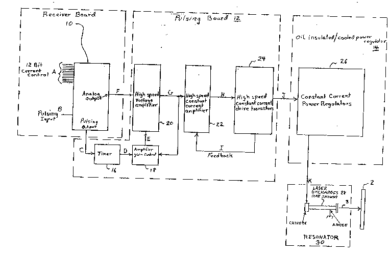
Fig. 4 is a ~loak diagram of a la~er apparatus which
can carry out the above described method. Fig. 5 ~hows
wave~orms at various points in the bloc~ diagram of Fig. 4.
~ s can ba seen in Fig. 4, the laser apparatus 1 com-
prises three high speed circuits shown as a receiver board
10, a pulsing board 12 and an oil insulated/cooled power
regulator 14. The receiver board 10 has high speed optical
link inputs for receiving twelve bit digital current control
sigr.als A and ~iber optic pulses B. These separate optical
links allow for the very fast rise times that are necessary
for carrying out the pulsing operation of the present
invention.
The receiver board 10 includes a digital-to analog
converter ~or con~erting the digital twelve bit current
control signal A into an analog output F to set the operating
current ~or the system. As can been seen from the waveform
diagram of Fig. 5, the receiver board 10 will also provide a
pulsing output C which corre~ponds to the pulsing input B,
9'~
with the level o~ the output being set by the receiver board
at a desired level. For example, Fig. 5 shows the pulsing
output C providing a 5 volt level when the fiber optic pulse .
input B is ON, and a O volt level when the fiber optic
lnput pulse B is OFF. 0~ aourse, these illustrated level6
are purely for purposes of examples, and di~ferent levels
could be set if desired.
The pulsing board 12 has five circuits, a precise timer
16, an amplifier gain control 18, a high speed voltage
amplifier 20, a high apeed constant current amplifier 22 and
a driver ~tag~ 24 co~prised of high 6peed constant ~urrent
drivlng transistors. The analog output F of the receiver
board 10 is applied to the input of the high speed voltage
amplifier 20. The pulse output C of the receiver board 10,
on the other hand, 18 applied to the timer 16 to produce a
tlmer output slgnal such as D shown in ~ig. 5. This timer-
output signal D,~ in turn, controls z gain control circuit
18. This gain control circuit 1~ is essentially an
electrical switch operated by feedback from the high speed
voltage amplifier 20 and the ti~er output D to generate a two
position sig~al E to apply to the voltage amplifier 20.
The high speed voltage amplifier 20 operates with its
analog input F and its gain control input E to produce an
output æuch a~ the pulsed signal G shown in Fig. 5. The
voltage levels of 5.49 volt and 1.83 volt shown there are
solely for purposes of example of a typical output fro~ the
amplifier 20. As can be seen there, the lower level of the
output G is not a O voltage level.
1 0
.
. .. . .. .
9^~
The a~pl~iar 20 output G i~ provided as one lnput to a
high speed constant current ampli~ier circuit 22. The other
input to this constant current amplifier 22 is a feedback
~ignal I ~rom the driver stage 24. This feedback signal I
will have the wave~orm shown in Fig. 5. Upon xeceiving
: these two inputs G and I, the constan~ curr~nt amplifier 22
will produca an output such as that shown by H in Fig. 5.
The output H o~ the ampli~ier 22 i5 applied to the
drlver stage 24~ This driver stage 24 is made up o~ high
speed translstors which will operate with the sign~l H ~o
produce an ampli~ied high voltage output J.
. The high voltage output signal H of the driver stage 24
is, in turn, applied to constant current power regulator 26
in the oil insulated/cooled power regulator 1~. This
constant current power regulator 26 will operate on the high
voltage signal J to produce the laser driving signal X having
a lower 75 ma lev~l with a pulsed 225 ma level. This laser
driving signal K will operate in conjunction with laser
discharges 28 of the CO2 laser resonator 30 (which converts
the electrical energy into the laser beam 3) to produce the
1, 000 Watt CW output of Fig. 3 when the signal K has the 75
ma level and the 3,000 Watt pulse level when the signal K has
the 225 ma level. In this example, the 1,000 Watt level can
be the maximum CW level, although the invention is not
limited to this.
An important aspect o~ the constant current power
regulators is that they are oil insulated. This oil insula-
tion allows for better cooling than can be obtained with air
11
.. .. . ............ . . . . ............ . .. .
.. .. .. . . .
.. .
~zg ~ ~9
insulation. This, in turn, allows shorter leads to be used
between the regulator 14 and the pulsing board 12. The
shorter lead length, in turn, permits a faster rise time than
would otherwlse be possible.
Regarding the operation of thQ cirGuitry shown in
Fig. 4, it should be noted that when the pulsing ~i~er optic
is pulsed to the receiver board 12, it, in turn, activates
the timer 16 which i~ set to an optimum pulse length ~or peak
laser power. ThQ pulse width is determined by using an
optical power detector ~not 6hown). The pulse length is
increased in length until the optical output from the
resonator 30 no longer increases and ~ust beg$ns to fall.
. During thi~ pulse width, tha gain of the high ~peed
voltage ampli~ier 20 i6 increased by an exact amount by the
ampli~ier gain control cirouit 18. This provides increased
drive to the high speed constant current ampli~ier 22 and
high speed constant current drive transistor in the drive
circuit 2~. This, in turn, increases the current to the
resonator 30 through the constant curr~nt power regulator 26
above the level set by the analog voltage. This is done ~or
a precise length o~ time for maximum ~eak laser power.
Fig. 6 provides a schematic illustration of a circuit
arrangement which can be used to construct the block diagram
o~ Fig. 4. As shown there, the analog output F from the
receiver board 10 is provided to the positive terminal of an
operational amplifier 32 in the high speed voltage amplifier
circuit 20 through a voltage divider. The pulse output C
~rom the receiver board 10 i8 applied to a timing circuit 34
12
09
ln the timer 16 through a level converter circuit. As shown
ln Fig. 6, the a~orementioned pulse duration adjustment for
the timer 16 is accomplished by using a RC cixcuit with a
varlable resistor. For purposes of example, the timing
circuit 34 can be constructed of a commercially available
timer identi~ied by the codes CD 4047.
~ he ou~put of the timing circuit D is, in turn, coupled
to a swit~h 36 in the amplifier ga~n control circuit 18. An
example of this switch 36 is sold under the code designation
CD 4066. Pulse amplitude adjustment is carried out by a
varîable rssistor arrangement in the feedback from the output
of the operational amplifier 32. The output of the switch 36
constitutes the gain control signal E that is coupled to the
negative input o~ the opexational amplifier 32 to control its
operation.
The high speed constant current amplifier 22 is ~ormed
of the operational ampli~ier 38 connected as shown to operate
as a constant current amplifier. Incidentally, the
operational amplifiers 32 and 38 can be constructed of the
same type of op~rational amplifiers, if deslred (with the
connection arrangements being different, of course, ~o
provide the desired di~ferent ampl~fying steps). One example
o~ a suitable operational amplifier is sold under the code
designation 741.
The output H of the operational amplifier 38 is applied,
in turn, to the input of a bipolar transistor 40 of the
driver cir~uit 24. As can be seen in Fig. 6, this translstor
4 0 is conneated to serve as a c:onstant current drive
13
tran~istor. A6 shown, the transi~tor 40 i~ coupled to
provide the *ee~b2ck ~ignal I ~rom its emitter to the input
of the operational a~plifier 380 It al~o provides the output
J across ~er~inals connec~ed to its collector and emitter.
Zener diodes 42 and a high voltage suppressor 44 ~which can
be formed of back-to-back Zener diodes) ~xe provided to
prevent damage to the power regulator 26 in case Or a voltage
~v~qe~
., lz~51~C ~
It should be noted that ~or simpllclty of illustration,
~zfi/~/~ only. single operational ~pli~rs are shown for the
a~plifiers 20 and 22, and only a single transistor is shown
for the driver circuit 24. It is to be understood, of
course, that plural operational amplifiers and transistors
would o~ten be used in actual practice depending upon the
power levels involved, especially ~or the constant current
amplifier 22 and the driver circuit 24.
As discussed earl$er, the constant rurrent power
regulators operate to convert the voltage output ~ from the
driver clrcuit 24 into a current signal K for controlling the
laser discharges to provide a power output 6uch as 6hown in
Fig. 3. Although ~he present invention is not limited to
this, the constant current power regulators ~6 can be for~ed
of beam power triode tubes connected together $n a constant
current configuration. These triode tubes will have their
~ilaments controlled by the output ~ ~rom the transistors 40
of the driver circuit 24. More specifically, as can be
appreciated by comparing the waveforms of J and ~ in F~g. 5,
the triode~ will operate such that as the filament winding o~
14
the tubes are pullsd down, the tubes will conduct to a
greater extent. In other words, the lower the voltage
outputs from the transistors 40 (i.e., the level o~ J), the
higher the current which will be produced from the triodes.
Therefore, the characteristics shown in ~ is obtained with
the high pulse spikes of 225 ma being generated when the J
output as iB at its low 25 Yolt level, and the constant 75 ma
level is obtained when the signal J is at its higher control
level of 75 volts. In the exa~ple shown, the pulse duration
~or the 225 ma level is approximately eq~lal to 0.125 msec,
although this, o~ course, can ~e varied as nec~ssary to
obtain the best laser output under the particular circum-
stances.
Although the present invention has been described in
detail with regard to t~e detail with the preferred em-
bodiment o~ the apparatus shown in Figs. 4-6, it is to be
understood that this is solely ~or purposes o~ example. In
other words, the present i~vention regarding the generation
of the laser power waveform shown in Fig. 3 is not limited
only to the preferred embodiments of Figs. 4-6, and other
circuit arrangements to arrive at this waveform could also be
used. Also, it is to be understood that modifications could
be made to the ~tructure o~ Figs. 4-6 themselves which would
still fall within the structure of the present invention.
While I have shown and descrlbed only one embodiment in
accordance with the present in~ention, it is understood that
the same is not limited thereto, but is susceptible of
numerous changes and modifications as known to those skilled
in the art. The method o~ the invention has applicability to
laser processing of ~atarials other than cutting, including
welding, surface ~inishing, machining, etc. Therefore, I do
not wish to be limited to the details ~hown and described
hereto~ but intend to cover all ~uch changes and
modi~ications as are encompassed by the scope of the appended
claims.
:
16