Note : Les descriptions sont présentées dans la langue officielle dans laquelle elles ont été soumises.
The present inyention relat~s to a single mode
optical waveguide of the type in which a cor~ glass portion
is embedded in a cladding layer disposed on a ~ubstrate.
In a silica single mode optical waveguide which
can be fabricated on a silica substrate or a silicon
substrate, its cross sec~ion has ~ size which can be
determined to be about 5-10~m so as to correspond to ~hat
of ~ conventional single mode optical fiber, so that the
silica single mode ~ptical waveguide is expected as means
for realizing practical waveguide type comp~nent parts
having an excell~nt matching characteristic with an ~ptic~l
fiber.
The optical waveguide of the type described is
disclosed in detail in Electronics Letters, 24 Oct. 1985,
Vol. 21, No. 20, pp. 1020-1021, "~IIGH SILICA SING~E-MODE
OPTICA~ REFLECTION BENDING AMD INTBRSECTING W~VEGUIDES" or
in Electronics Letters, 13 March 1986, Vol. 22, No. 6, pp.
321-322, "LOW-LOSS HIGH-SI~ICA SINGLE MODE CHANNEL
WAVEGUlDES".
There is known a conventional silica sin~le mode
optical wavegu;de ha~ing a silica glass substrate, a
silica glass core portion and a silica glass cladding
layer surrounding the core portion. The cross sectional
size of the core portion is about lQ micrometres. The
thickness of the substrate is of the order o~ 2mm. Such
silica single mode optical waveguide can be fabricated by
a combination of deposition technique for depositing a
glass film by flame hydrolysis of raw material gases such
as SiC14, TiC14 or the like with reactive ion etching
technique. For instance, reference is made to MICROOPTICS
NEWS, 1986, 4/15, Vol. 4, No. 2, pp. 33(108)-38(113),
S "Microlithograpy of High-Silica Channel Optical
Waveguides".
In the conventional silica single mode optical
waveguide described above, tensile stresses are imparted
to the inside of the film surface of the cladding layer
because of the difference in thermal expans;on coefficient
between the cladding layer and the silica glass
substrate. That is, it exhibits stress-induced
birefringence and, in general, a value of stress-induced
birefringence B is of the order of 10 5.
The birefringence in an optical waveguide is one
of important factors which determines performance of a
waveguide type optical component part, 50 that it is
desired that a birefringenae value is controlled with a
high degree of accuracy. However, ln a conventional siliaa
single mode waveguide, there is no way to vary or control a
birefringence value except to change glass compositions or
kinds of the substrate. In addition, directions of the
principal axes of stress are limited to the direction in
parallel with the surface of the substrate and to the
direction perpendicular thereto. In addition, it is
difficult to vary locally birefringence properties in the
optical waveguides. Therefore, these problems constitute
obstacles in case of fabricating a waveguide type op~ical
component which exhibits a high degree of per~ormance.
~4~
In some cases, instead of silica ~lass, silicon
is used as the substrate. In this case, the cross
sectional size of the core portion is about 10 micrometres
also in the case of silicon substrate. The thickness o
the cladding layer is of the order of 50 micrometres. The
thickness of the silicon substrate is of the order of 0.4
through lmm.
In the case of a silica single mode optical
waveguide fabricated on a silicon substrate, a ~trong
compression stres`s of the order of 15 kg/mm2 is applied to
the interior of the glass film surface due to the
difference in thermal expan~ion coefficient between the
silica glass and the silicon substrate, so that the optical
waveguide exhibits stress-ir.duced birefringence.
Birefringence of an ~ptical waveguide is one of important
actors which determine performance of a waveguide type
optical component part. Therefore, it is desired that the
birefringence is controlled with a high degree o~ accuracy.
In general, a value of birefringence is of the o~der of
10-4, so that it is di~ficult to remove adver~e effec~s of
the stress from the silicon substrate~ This problem also
constitutes an obstacle in a ca~e of fabrica~ion of a
waveguide type optical component.
Furthermore, in a case of the conventional
structure described above, in which a core portion
constituting a main bod~ of an optical waveguide is
completely made into intimate contact with a silicon
substrate via a cladding layer, it is complet~ly
impossible to mechanically move the main body of the
optical waveguide on the substrate. This problem also
constitutes an obstacle when a variety of funckions can be
realized by an optical waveguide.
Meanwhile, as to ~ struc~ure of an optic~l
fibers, there ls disclosed in, for instanee, Journal oE
Lightwave Technology, Vol. LT-l, No. 1, March 19~3, pp. 38-
43, "Fabrication of Polarization-Maintaining and
Absorption-Reducing Fibers", an optical fiber which
maintains polarization properties by providing a stress
applying portion surrounding a core portion in a eladding
layer. In the optieal fiber, however, it is impossible to
locally adjust a stress in the longitudinal direetion of
the waveguide.
An optieal eireuit diselosed in Laid-Open
Japanese Patent Applieation No. 196,204/1982, stress
birefringenee is adjusted by varying a width of a ridge in
a YIG optieal waveguide (ridge type) on a GGG substrate to
coincide a transmission phase constant of a TE wave with
that of a TM wave~ If, however, the ridge width is varied,
the structure of the eore portion is varied, so that a spot
size of the transmitted light is also varied. That is,
birefringenee eannot be adjusted independently of a core
structure.
Laid-Open Japanese Patent Applieation No.
4,022/1982 dlseloses a method for produeing stress-induced
birefringenee in a ridge type optieal waveguide by loadin~
a dielectrie film (SiO2 film) on a ridge type YIG optical
waveguide. If, however, the dielectrie film is loaded on
the ridge type optieal waveguide~ not only the stress-
induced birefringence but also the structure of the eore
portion itself are eonsiderably varied. Therefore, as in
the ease of Laid-Open Japanese Patent Application Mo.
196,204/1982, the birefringence cannot be adjusted
independently of a structure oE the core portion,
In view of the above, it is an object o the
present invention to provide a silica single mode optical
waveguide which overcomes the above-described obstacles and
restrictions to control birefringence more flexibly,
It is another object of the present invention to
provide a silica single mode optical waveguide in which
polarization properties can be locally controlled along the
optical waveguide,
It is a further object of the present invention
to provide a silica single mode optical waveguide which
overcomes the above-described obstacles and restrictions
due to a silicon substrate so that birefringence can be
locally removed.
It is still a further object of the present
invention to provide a silica optical waveguide fabricated
on a silicon substrate in such a way that a portion of the
optical waveguide can be locally di~placed with respect to
the silicon substrate, so that the optical waveguidq can
reali,ze various functions as described above.
It is yet a Eurther object of the presqnt
invention to provide an optical waveguide in which
birefringence can be adjusted by adjusting a stress to be
applied to the optical waveguide,
It is yet still a further object of the present
invention to provide an optical waveguide in which a s~ress
adjusting portion is provided in a portion of a cladding
layer independently of a structure of a core portion.
6~
In the first aspect of the present invention, a
silica optical waveguide comprises~
a substrate;
a cladding layer formed on the substrate,
a silica glass core portion ormed in the
cladding layer; and
stress adjusting means provided in the cladding
layer in the vicinity of the core portion or adj usting a
stress applied to the core portion to adjust stress-induced
birefringence in the core portion.
Here, the stress adjusting means may comprise a
member which applies a stress to th~ core portion~
The member may be an elongated member which is
embedded in the cladding layer and may be composed of a
material having a thermal expansion coefficient different
from that of the cladding layer.
The material may be selected from a group
consisting of silicon, silicon nitride and B2O3 doped
silica glass.
A substrate may be composed of a silica or
silicon substrate.
The stress adjusting means may be a groove or
relieving the stress.
The groove may be defined only in the cladding
layer.
The groove may have such a depth that the bottom
of the groove reaches the inside of the major surface of
the substrate.
-- 7 --
A portion of the op~ical waveguide constitute~ by
the core portion which is surrounded by the cladding layer
may be separated from the major surface of the substrate
A portion of the cladding layer corresponding to
one portion of the optical waveguide may be removed to form
at least one pair of grooves and a portion of the silica
substrate corresponding to the portion of the optical
waveguide may be removed to form a recess communicatiing
with the at least one pair of grooves.
A plurality of pairs of groove may be provided
through bridge structures in the recess in the longitudinal
direction of the core portion.
A portion of the cladding layer corresponding to
one portion of the optical waveguide may be removed to form
a plurality of grooves in the longitudinal direction of the
core portion and a portion of the silicon substrate
corresponding to the portion of the optical waveguide may
be removed to form a plurality of recesses which
communicate with the plurality of pairs of groove,
respectively, in the longitudinal direction of the core
portion.
A portion of the portion of the optical wave~uide
corresponding to one end of the at least one pair of
grooves may be cut out to form a separation groove
communicating with the recess and the at least one pair of
grooves.
The substrate may be a silicon substrate and the
recess may be formed by a selecting etching process through
the at least one pair of grooves.
In the second aspect of the present invention, a
waveguide type Mach-Zehnder interferometer comprise~;
two optical couplers;
two optical waveguides having different lengths
and exhibiting s~ress-induced birefringence, the two
optical waveguides coupling the two optical couplers,
respectively;
stress relief grooves disposed along and on both
sides of at least one optical waveguide in such a way that
a difference in values obtained by line integration of a
birefringence value with respect to each of the at least
one optical waveguide between the two optical couplers is
substantially equal to an integer multiple of a wavelength
of light used.
Here, each of the optical waveguides may be a
single mode optical waveguide comprising a silicon
substrate, a silica cladding layer disposed on the silicon
substrate and a core portion embedded in the cladding layer
and the stress relief groove may be provided along the core
portion.
A phase shifter Eor vary:ing an effectlve op~ical
path length of one of the two optical waveguides may be
disposed on the one of the two optical waveguides.
The phase shifter may comprise a thin film
heater.
The phase shifter and the stress relief grooves
may be disposed along the same or different optical
waveguides.
In the third aspect of the present invention, a
waveguide type optical phase plate comprises:
a single mode optical waveguide having a
substrate, a cladding layer formed on the substrate and a
core portion embedded in the cladding layer; and
at least one stress adjusting member disposed
along the core portion by a predetermined length in at
least one portion of the cladding layer in such a way that
the principal axes of birefringence of the optical
waveguide are inclined with respect to the direction
perpendicular to or in parallel with the major surface of
the substrate.
Here, ~he stress adjusting member may be a stress
relief groove.
The substrate may be a 5ilicon substrate and the
single mode optical waveguide may be a silicon single rnode
optical waveguide.
A plurality of stress relief grooves may be
sequentially disposed along the core portion and
alternately on both sides o~ the core portion.
~ spacing between the stress relie~ groove and
the core portion may be varied in the longitudinal
direction o the core portion.
A depth of the stress relief groove may be equal
to or smaller than the thickness of the cladding layer.
The above and other objects, effectsy features
and advantages of the present invention will become more
apparent from the following description of preferred
embodiments thereof taken in conjunction with the
accompanying drawings.
-- 10 --
Figure 1 is a sectional view showing an example
of a prior art silica optical waveguide, as described
above;
Fig. 2 is a eectional view ~howing one embodiment
of a sil$ca optical waveguide in ~ccordance with the
present ~nvention;
Fig~ 3 is an explanatory diagram used to explain
a dis~ribu ion of stress in the embodiment shown in Fig. ~;
Figs, 4A-4E are sectional views ~howing an
10 embodiment o ~teps of ~abrication of the e~bodiment of the
optical waveguide shown in Fig. 2;
Figs. 5-B are ectionAl views ~howing other
emboc`.iments of the present invention, re~pectively;
Figs~ 9A and 9B are a plan view and an enlarg2d
~15 sectional view, respectively, showing one embodiment of a
waveguide type optical phase plate constructed by an
~ptical waveguide in accord~nc~ with the present invention;
Fig~ 10 is a sectional view showing a further
embodiment of a silica optical waveguide in accoraance with
the present invention;
Fig. 11 illustrates'a predicted ~harac~eristic
curve of bir~frlngence values obtained by a definite
element method;
Figs. 12A~12D are sectional view5 showing one
embodiment of steps for fabricating the optical waveguide
shown in Fig. 10;
Figs. 13l 14 and-15A-15E are sectional views
showing further embodiment6 of an optical waveg~lide in
accordance with the present ~nvention;
- 11
. ~ .,
Fig, 16 is a plan view showing a ~urthe~
embodiment of an optical waveguide in accordance with the
present invention;
E'igs. 17A and 17B are perspective views showing
further embodiments of an optical waveguides in accordance
with the present invention;
Fig. 18A is a plan view showing a further
embodiment of an optical waveguide in accordance with the
present invention;
Fig. 18B is a sectional view taken along line A-
A' in Fig, 18A;
Figs, l9A and l~B are a plan view and a partially
enlarged plan view showing an optical frequency multiplex
circuit in accordance with the present invention;
Fig. 20A is a plan view showing a modification
thereof;
Fig, 20B is a sectional view taken along line
C-C' in Fig. 20A;
Fig, 21A is a plan view showing a further
embodiment of the present invention;
Fig. 21B is a sectional view ta!cen along llne C-
C' in Fig. 21A;
Fic3. 22A is a plan view showing a conventional
waveguide type Mach-%ehnder interferometer;
Fig. 22B is a sectional view taken along line ~-
D' in Fig. 22A;
Fig, 23A is a plan view showing an embodiment of
a waveguide type Mach-Zehnder interferometer in accordance
with the present invention;
~ 12 -
.6~
Fig. 23B iB a ~ectional view taken along lirle ~-
E' in Fig. 23A;
Fig. 24 is a plan view ~howing a modi~i~ation
thereof;
Fig. 25 is an explanatory diagram u~ed to explain
a conventional bulk ~ype ~ptical phase pla'ce ta half-wave
plate );
Fig. 26 is a sectional view showing an embodiment
of an optical phase plate in ar~cordance with he present
i nve nti on;
Fig . 27 ~ s ar~ explanatory ~lagram used ~ explain
operations sf a s~ress relief groove ~hereof;
Figs. 28 and 29 are plan views showing ~wo
embodiments, respec~ively, of an optical phase plate in
1~ accordance with the present invention;
Figs. 30A~30F are expl~natory diagrams used to
explain operations of the optical pha3~ plate shown in
Fig . 29;
F~g. 31 i~ zl plan s~lew showirlg an ~mbodimen~ of
stress relie~ groove; and
Fig~ 32 i~ a ~ection~l view ~howing ~nother
embodiment o~ a stress relief groove,
Embodiment 1:
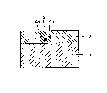
Figure 1 is a cros~ sectiorlal YieW showing a
structure of a conventional silica single mode optical
waveguide. Reference numeral 1 designates a ~ilica glass
substrate; 2, 2 silica glass core portion an~ 3, a silica
glass ~ladding layer surrounding the cor0 portion 2.
Fig. 2 is a setional view shQwi~g a fir~t
embodiment of a ~ilica single mode opt;cal waveguide
stress applying portions in accordance with the present
invention. A structure in which a cladding layer 3 is
disposed o~ a ~ilica substrate 1 and a core por~ion 2 is
embedded into the claddin~ layer 3 is substantially similar
- 13 - -
to that of the conventional optical waveguide shown in E'ig
1, in the present embodiment oE the present invention,
stress applying portions 4a and 4b composed, for example,
of silicon, are disposed in the vicinity of the core
portion 2.
Fig. 3 is an explanatory diagram used to explain
a stress distribution around the core portion 2 shown in
Fig. 2. After the fabrication steps at high temperatures
to be described in more detail below, tensile stresses act
on the core portion 2 at room temperature due to
differences in thermal expansion coefficient between the
core portion 2 and the silicon stress applying portions 4a
and 4b. In a case of the optical waveguide in which the
core portion 2 was lO~m x lO~m and the silicon stress
applying portions 4a and 4b were lO~m x 17~m and a distance
between the core portion 2 and the silicon stress applying
portion 4a or 4b was 12~m, a measured birefringence B was
1.5xlO 4. This value was about five times as high as the B
value of the optical wavegu:ide fabricated on the silica
substrate 1 without providing a stress applying portion
Thus, it was conEirmed that the silicon stress applving
portions 4a and 4b affect a value of B.
FigS. 4A-4E show an embodiment of steps for
fabricating the silica single mode optical waveguide with
the stress applying portions 4a and 4b of the type
described above with reference to E'ig 2.
First, as shown in Fig. 4A, a silica optical
waveguide film consisting of a lower cladding layer 31 and
a core layer 32 is deposited on the s~rface of the silica
- 14 -
glass substrate 1. rrhen~ an undersired o~ the core layer
32 is removed by a reactive ion etching process to define
the core portion 2 in the Eorm of ridye, as shown in Fig.
4B.
Thereafter, as shown in Fig. 4C, an intermediate
cladding layer 33 is deposited in such a way that the core
portion 2 is embedded in the intermediate cladding layer
33. 5ubsequently, an amorphous silicon (a-Si) layer is
formed on the surface of the intermediate cladding layer 33
by a high speed sputtering process. Next, an undesired
portion is removed by an etching process to form the stress
applying portions 4a and 4b.
Finally, as shown in Fig. 4E, an upper cladding
layer 34 is deposited in such a way that the stress
applying portions 4a and 4b are embedded therein. Then,
the thus laminated structure is subjected to a heat
treatment process at a high temperature (between 1100-
1200C). As a result, a-Si is converted into
polycrystal~ine silicon and during the step Eor cooling
the optical waveguide thus fabricated to room temperature,
stress-induced birefringence is produced as shown in Flg
3.
Embodiments 2-5:
Figs. 5-8 are sectional views showing a second
embodiment, a third embodiment, a fourth embodiment and a
fifth embodiment~ respectively, in accordance with the
present invention.
- 15 -
~9q~6~
In the second embodiment as shown in Fig. 5, a
stress applying portion 14 is provided above the core
portion 2 within the cladding layer 3, so that the
compression stress is imparted to the lower core portion 2
from the stress applying portion 14 and consequently a high
degree of birefringence having a sign opposite to that of
birefringence of the first embodiment is produced.
In the third embodiment as shown in Fig. 6, the
stress applying portion 14 is provided at a position
obliquely upwardly of the core portion 2. In this
embodiment, stress-induced birefringence having the
principal axis inclined at 45~ with respect to the main
surface of the substrate 1 can be obtained.
In the fourth embodiment as shown in Fiy. 7,
stress applying portions 14a and 14b are disposed on both
sides of the core portion 2 by a combination of a
deposition process and an etching process.
In the fifth embodiment as shown in Fig. 8, the
stress applying portions 14a and 14b are defined on both
sides oE a directional coupler composed of two aore
portions 2a and 2b. In this embodiment, a coupling
coef~iclent o~ the directional coupler is dependent on
polarization.
In the above described embodiments, the stress
applying portions 4a, 4b, 14, 14a and 14b are composed of
silicon, but it is to be understood that any material can
be used as far as it will not react with silica glass at a
high temperature and which has a thermal expansion
coefficient different from that of the surrounding sillca
i
- 1.6 -
glass. For instance, platinum, silicon nitride or the :L:ike
may be used. Furthermore, glass which is considerably
diEEerent in composition from the silica glass Eorrning the
core portion 2 or the cladding layer 3~ for example, si.lica
glass containing a large amount of B2O3 deposited by, for
instance, a CVD process may be used. However, it is not
preferable to form a stress applying portion by glass
containing an alkali metal, because the surrounding silica
glass is crystallized.
In the fabrication steps shown in Figs. 4A-4E, an
a-Si layer is often used as an anti-etching mask having
resistance to etching when an optical waveguide film is
formed by a reactive ion etching process, so that in some
case, after the etching step, a part or whole of the anti-
etching rnask can be left unremoved and embedded into the
upper cladding layer 34, so that the unremoved anti-etching
mask defines the stress applying portions 4a and 4b.
So far, the substrate 1 has been described as
consisting of silica glass, but it is of course apparent
that the stress applying portion or portions are effective
as means or controlling bireringence, even wh*n ~ .silicon
substrate is used as the substrate 1. In the case o:E the
silicon substrate, it rnust be taken into consideration
that, unlike the silica glass substrate, the opt.ical
waveguide receives as a bias force a high degree of
compression stress (corresponding to a birefringence value
of the order of 10-4) as a whole.
It is of course possible to positiorl the stress
applying portion or portions at a desired position or
- 17 -
positions in the longitudinal direction of the optical
waveguide.
As described above, in the first to fifth
embodiments, the stress applying portions 4a, 4b, 14, 14a
and 14b are disposed in the vicinity of the core portions
2, 2a and 2b within the cladding layer 3, a degree of
birefringence in the optical waveguide can be precisely
controlled by varying the position and shape of the stress
applying portion. Therefore, the present invention is
remarkably useful in a case of fabricating an op~ical
waveguide type optical component part to be used in an
optical sensor or a coherent optical communication system
in which polarization characteristics of the component play
a very important role.
~mbodiment 6:
Figs 9A and 9B show an embodiment of a waveguide
type optical phase plate constructed by an optical
waveguide in accordance with the present inventlon.
Fig~ 9A is a plan view thereof, while Fiy 9B is
a sectional view, on englarged scale, taken alorlcJ line A~A'
in Fig. 9A. The silica core portion 2 (lO~m x lQ~m) and
the polysilicon stress applying portions 14a and 14b (lO~m
x lO~m) are embedded into the silica cladding layer 3
(approximately 70~m in thickness) formed on the surface of
the silica glass substrate 1~ The stress applying portions
14a and 14b are disposed on both sides of the core portion
2 and are spaced apart f rom the center of the core portion
2 by a distance S in a diagonal direction, which the
- 18 ~
portions 14a and 14b are extended alony the core portion 2
by a distance Q.
Such a structure can be fabricated by a
combination of a deposition process and an etching process.
Due to the stress applying portions 14a and 14b, a tensile
stress acts on the core portion 2 in a diagonal direction
thereof. Here, a direction of the principal axis of
stress-induced birefringence can be varied by selecting the
distance S. In this embodiment, the distance S is l9~m, so
that the directîon of the principal axis of stress-induced
birefringence is inclined by 45 with respect to the major
surface of the substrate 1. In the case, a magnitude B of
stress-induced birefringence is of the order of O.~x10-4
and the distance Q is so selected to satisfy the following
relation:
B-Q = ~/2
, where ~ is a wavelength of light used. For instance, the
length Q of each of the stre~s applying portions 14a ancJ
14b becomes 5mm when ~ i5 1.3~m. As a result, the optical
waveguide with the ~tress applying portions as shown in
Fig~. 9A and 9B functions as a half wave plate having the
optical axis inclined by 45 with respect to the major
surface of the substrate 1. When a linearly polarized TE
wave ~having an electric field direction in parallel with
the major surface of ~he substrate 1) is incident to the
core portion 2 from the left end of the optical waveguide
shown in Fig. 9A, the light beam passes through the stress
- 19 -
applying region formed by the stress applyiny portions 14a
and 14b, so that a direction of polarization o the liyht
beam is rotated by 45x2=90, and then the light beam is
emitted from the right end of the core portion 2 as TM wave
(having an electric field perpendicular to the major
surface of the substrate 1). Thus, the optical waveguide
shown in Figs. 9A and 9B functions as a TE/TM mode
converter. In addition, in accordance with manners of
setting values of S and ~, various waveguide type optical
phase plates such as a half wave plate, a quarter wave
plate or the like having an optical axes extended in
various direction can be realized.
Embodiment 7:
Next, the present invention will be explained
with reference to an embodiment thereof in which a stress
relief groove or grooves are formed in the cladding layer 3
adjacent to the core portion 2 in order to control the
birefringence o~ the optical waveguide. rrhe stres~ relief
grooves may be arranged on both sides of the core portion
in symmetric relationship with the core portion 2 or only
one stress relief groove may be arranged only on one side
of the core portion 2. Birefringence of the optical
waveguide can be controlled by suitably selecting the
position, the depth and the width of the stress relief
groove.
Fig. lO illustrates a seventh embodiment of the
present invention in which, unlike the prior art optical
waveguide shown in Fig. l/ open grooves 5a and 5b are
- 20
6~
formed along the core portion 2 on both sides thereof and
in symmetric relationship with respect to the core portion
2 within the cladding layer 3. The cladding layer 3 is
50~m in thickness and consists of SiO2 glass. The core
portion 2 consists of SiO2-Tio2 glass and has a cross
section of 8~m x 8~m. The height of its center axis is
25~m from the major surface of the Si substrate l. The
grooves 5a and 5b are 150~m in width and are formed on both
sides of the core portion 2, while leaving the cladding
portion 3a with a width W around the core portion 2.
Fig 11 illustrates the dependence of a
normalized birefringence B/Bo (where Bo represents a value
of birefringence when both the grooves 5a and 5b are not
formed) of the optical waveguide shown in Fig. 10, obtained
by the analysis of the stress distribution of the optical
waveguide.
As the width W becomes wider, a value B of
birefringence of the optical waveguide approaches to a
predetermined value Bo, which is dependent mainly upon a
diEference in thermal expansion coefficient between sillca
glass and the Si substrate. On the other hand, when the
width W becomes narrow, the value of B is decreased. For
instance, when W=100~m, B/Bo is decreased to be almost
equal to 0.25. Therefore, Fig. ll shows that a
birefringence value B o the optical waveguide can be
determined to be a desired value by varying the positions
of the grooves 5a and 5b which are represented by the
parameter W. It should be noted that if necessary, a
birefringence value can be made almost equal to zeroO
- 21 -
4~
Figs 12A-12D show an embodiment of sequential
steps for fabricating the silica single mode optical
waveguide with stress relief grooves as shown in Fig, 10.
First, as shown in Fig. 12A, a silica optical
waveguide consisting of a lower cladding layer 41 and a
core layer 42 is deposited on one major surface of an Si
substrate l. Next, as shown in Fig. 12B, an undesired
portion of the core layer 42 is removed by a reactive ion
etching process to form a ridge-shaped core portion 2.
In the step shown in Fig. 12C, an upper cladding
layer 43 is deposited to embed the core portion 2 therein,
so that the cladding layer 3 is formed together with the
lower cladding layer 41.
Finally, as shown in Fig. 12D/ grooves 5a and 5b
for relieving residual stress are recessed along the core
portion 2 in the cladding layer 3 by a reactive ion etching
process. As a result, the optical waveguide as shown in
Fig. 10 is obtained.
A rneasured value B of birefringence wa~ l.lx10-4
in the case that the optical waveyuide (W=lOOIlm) havLny th0
structual parameters as shown in Fig. 10 was ~abricated.
In the case of the optical waveguide in which no groove was
formed, a birefrinyence value Bo was 4.0x10⁻⁴. Therefore,
these values obtained by the practical measurements closely
coincide with the results oE the theoretical analysis by
the definite element method shown in Fig. ll.
In the above-described embodiment, while the
width of the grooves 5a and 5b is determined to be 150~m,
it should be noted that when the groove width is greater
than lOO~m, the dependence of the value B on the yroove
width is negligibly small. In some ca5e, the groove width
may be infinite. That is, one .side of one groove 5a or 5b
which is remoted ~rom the core portion may be open~ended.
Embodiment 8:
While in the embodiment shown in Fig. 10, the
grooves 5a and 5b reach the surface of the substrate 1, a
depth of the grooves Sa and 5b can be adjusted, as shown in
Fig. 13, to control a birefringence value B of the optical
waveguide. A method in which a value B is measured while
the grooves 5a and 5b are being formed by a reactive ion
etching and the etching process is interrupted when a
desired birefringence value B is obtained is effective to
precisely obtain a desired birefringence.
Embodiment 9:
Fig. 1~ shows a further embodiment of the present
invention in which a stress relief groove 64 is formed only
on one side of the core portion 2. ~ compression stress
can be produced adjacent to the core portion 2 in a
diagonal direction, as indicated by the broken lines in
Fig. 14. This embodiment is ef~ective when it is desired
that a direction of the principal axis of birefringence of
the optical waveguide is off a direction perpendicular to
or in parallel with the major surface o~ the substrate 1.
- 23 -
Embodiments 10-14:
The cross sectional configuration oE the stress
relief groove is not limited to rectangle as described
above and can be varied as shown in Figs. 15A-15E.
In Fig. 15A, after the grooves which reach the
major surface of the substrate 1 are formed on bath sides
of the core portion 2 in the cladding layer 3, the bottoms
of the grooves 5a and 5b are further recessed into the
region of the substrate 1 to form the grooves 5a and 5b,
each having a depth deeper than the thickness of the
cladding layer 3.
In Fig. 15B, after the grooves which reach the
major surface of the substrate 1 are formed, the optical
waveguide ls immersed in a wet etching liquid (for
in5tance, a mixture of hydrofluoric acid, nitric acid and
acetic acid), so that desired regions of the Si substrate 1
including the regions immediately below the cladding layer
3 are etched out to form the stress relief grooves 5a and
5b. Both of the embodiments shown in Figs. 15A and 15B
have a hiyh degree o stress relieving efEect, as compared
with the optical waveguide in which the Si substrate 1 is
not etched at all.
Fig. 15C shows an optical waveguide in which the
stress relief grooves 5a and 5b are formed by a wet etching
process using hydrofluoric acid instead of a reactive ion
etching process. In the case of etching, the surfaces of
the cladding layer 3 except the portions in which the
stress relief grooves 5a and 5b are formed are protected by
silicon nitride film as a mask which has resistance to
- 24 -
etching with hydrofluoric acid. rrhis etching process is
simpler than reactive ion etching process, ~ut has a
problem that the etching control is rather difficult.
In the embodiments shown in Fig. 15D and Fig
15E, a reactive ion beam etching process which is a kind of
the reactiving ion etching processes is used. The major
surface of the substrate 1 is inclined with respect to the
direction of the ion beam so as to perform etching, so that
a stress relief groove 64 which is inclinecl at an angle
with respect to the major surface of the substrate 1 i5
formed in the cladding layer 3. These embodiments are
effective when it is desired that the direction of the
principal axis of birefringence in the optical waveguides
is determined to be off a direction perpendicular to or in
parallel with the ma~or surface of the substrate 1.
Embodiment 15:
In the embodiments 7-14 described above, it is
not needed that the stres6 relief grooves 5a, 5b and 6~ are
defined uniformly a].ong the core portion 2 of the optical
waveguides. It is of course possible to distribute the
groove at a desired position along the core portion 2 ~5
shown in Fig. 16. The arrangment as shown in Fig. 16 is
effective especially when it is desired to locally vary
birefringence characteristics in the optical waveguide.
Embodiment 16:
In the embodiments described above, a structure
of a single mode optical waveguide prior to the formation
of stress relief groove is such that the core portion 2 is
completely embedded or buried in the cladding layer 3 and
the upper surEace of the cladding layer 3 is substantially
flat. It is, however, to be understood that the present
invention is not limited to such a structure FigO 17B
shows an embodlment in which the stress relie~ grooves 5a
and 5b are formed in a single mode optical waveguide in
which the core portion 2 is covered with a relatively thin
cladding layer 13, so that the surface of the cladding
layer 13 is not flat. Fig. 17A is a perspective view of
this embodiment prior to the formation of the stress relief
grooves, while Fig. 17B is a perspective view thereof after
the stress relief grooves 5a and 5b have been formed.
The structure as shown in Fig~ 17B can be
fabricated by a conventional process in which the core
portion 2 is coated with a relatively thin glass layer (a
few ~m in thickness) by a CVD or sputtering process in a
step succeedincJ the step sh~wn in Fig. 4B in the
fabrication of the optical waveguide in accordance with the
sequential steps as shown in Figs. 4A-4E. ~Iere, r0Eerence
is made to A, Hlmeno et al., Electron Lett~, Vol. 21, No.
20, pp. 1020-1021, (1985). Fig. 17B shows the stress
relief grooves 5a and 5b which are ~ormed on both sides of
the core portion 2 of the optical waveguide as described
above in such a way that the bottoms of the stress relief
grooves 5a and 5b reach the major surface of the Si
substrate. The stress-induced birefringence
characteristics of the core portion 2 can be controlled by
suitably adjusting or selecting a position, a width, a
- 26 -
length or the like of the stress relieE grooves 5a and 5b,
like as in the cases o the above-described embodiments.
It is of course possible to provide the stress relief
groove only on one side of the core portion 2 50 that the
direction of the principal axis of birefringence is varied.
In the embodiments 7-16, it has been described
that the silica single mode optical waveguide is fabricated
on the silicon substrate, but it is of course possible that
the present invention may be equally applied to other
single mode optical waveguide composed of other material,
for example, an optical waveguide fabricated on a multi-
composition series glass substrate by an ion diffusion
process as long as the optical waveguide receives a stress
from the substrate.
As described above, according to the present
invention, the stress relief groove is formed along the
core portion of the optical waveguide in predetermined
portions of the cladding layer thereof, so that a
birefringence value of the optical waveguide can be easily
controlled
That i5, according to the preæent invention,
birefrLngence can be controlled only by the formation of
grooves without changing a composition of glass and a kind
of substrate In addition, birefringence can be controlled
selectively only at a predetermined position along the
optical waveguide on the substrate and, if required, the
principal axis of stress can be selected in a direction
other than a direction in parallel with or perpendicular to
the major surface of the substrate
~3~
ThereEore, according to the present invention, a
waveguide type component such as a quarter-wave plate, a
half-wave plate, a polarizer, a directional coupler, an
interferometer, a ring resonator or the like which is used
in a coherent optical communication system or optical
sensor in which polarization characteristics play an
important role, can be fabricated with a high degree of
accuracy.
Embodiment 17:
When a silicon substrate is used as the
substrate 7 it is possible to remove a portion of the
silicon substrate by, for instance, an etching process in
such a way that a portion of an optical waveguide having a
silica cladding layer formed on the silicon substrate and a
core portion embedded or buried into the cladding layer is
separated from the silicon substrate
A 17th embodiment having the above-described
structure is shown in Fig. 18A and Fig. 18B. FigO 18A is a
plan view, while Fig 18B is a cross sectlonal view taken
alon~ line ~~A' in Fig~ 18A.
As is apparent from Figs. 18A and 18B, the
cladding layer 3 is deposited on the silicon substrate 1
and the core portion 2 as the main body of the optical
waveguide is embedded in the cladding layer 3~ The grooves
5a and 5b are formed on both sides of and along the core
portion 2 in such a way that the bottoms of the grooves 5a
and 5b reach the major surface of the silicon substrate 1.
A portion of the silicon substrate 1 is removed by a
- 28 -
chemical etchlng process through the grooves 5a and Sb~
Therefore, there is provided a separated optical waveguide
7 in which the optical waveguide containing the core
portion 2 is separated from the silicon substrate 1 in a
region 6 where the silicon substrate 1 is removed.
Therefore, adverse effects upon the optical waveguide
portion 7 from the silicon substrate l can be minimized.
In the embodiment of the type shown in Figs. 18A
and 18B, the cladding layer 3 was 50~m in thickness and
composed of SiO2 glass. The core portion 2 consisted of
SiO2-Tio2 glass having a square cross section of 8~m x 8~m
and the height of the center position of the core portion 2
from the major surface of the silicon substrate 1 was 25~m.
Both the grooves 5a and 5b are 50~m in width and the
separated optical waveguide portion 7 interposed between
the grooves 5a and 5b was 50~m in width.
The grooves 5a and 5b were formed by removing
predetermined portions of the cladding layer 3 by a
reactive ion etching process and thereaEter the silicon
substrate 1 was immersed in isotropic etchant Eor silicon
for about ten minut0s so that the predetermined portion 6
of the silicon substrate :L was removed by a selective
etching process. The etchant used in this embodiment was a
mixture of 9ml hydrofluoric acid, 75ml of nitric acid and
30ml of acetic acid.
Birefringence of the optical waveguide of the
type described above with reference to Figs. 18A and 18B
was evaluated by polarization measurement As a result,
the birefringence B of the separated optical waveguide
- 29 -
portion 7 corresponding to the region 6 where the silicon
substrate 1 was removed was as low as 10-5, which is
considerably lower than a birefringence value B of 4x10⁻⁴
in the portion of the silicon substrate 1, which was not
rernoved by etching. Thus, it was confirmed that the stress
is relieved by separating the optical waveguide portion 7
from the silicon substrate 1.
Embodiment 18:
Figs. l9A and l9B show a specific embodiment of
an optical frequency multiplexing circuit which embodies
the present invention and which is polarization-
insensitive.
Fig. l9A is a plan view of the optical frequency
multiplexing circuit which comprises an SiO2 cladding layer
26 formed on a silicon substrate and two single mode core
portions 24 and 25 embedded in the cladding layer 26. The
two core portions 24 and 25 are partially very closely
spaced apart ~rom each other and in parallel with each
other to form directional couplers 22 and 23. The
directional couplers 22 and 23 have structural parameters
which aee so selected that a coupling eficiency is about
50~. The two core portions 24 and 25 which couple the
directional couplers 22 and 23 to each other are diEferent
in length by ~L. The sîlicon substrate is partially
removed to form a recess region 27 which is extended along
a part of the longer core portion 24 by a distance equal to
~L in the silicon substrate. A value of birefringence of
the separated optical waveguide portion 7 corresponding to
this recess region 27 is substantially equal to zero.
- 30 -
The length ~L; that is, the length of the recess
region 27 in the silicon substrate (corresponding to the
length of the separated optical waveguide portion 7) i.s as
long as a few mm or more. Therefore, it is necessary to
prevent damage to the optical waveguide portion 7. Thus,
as shown at enlarged scale in Fig. l9B showing the recess
region 27 defined in the silicon substrate, the recess
region 27 is divided into a plurality of sections of
grooves 27a and 27b for removing predetermined portions of
the silicon substrate which are disposed along the optical
waveguide portion 7 in the longitudinal direction thereof.
Therefore, the separated optical waveguide portion 7 is
supported by a plurality of bridge structures 28.
In this embodiment, the cross sections of the
core portions are equal in size to that of the first
embodiment. Each of the divided sections of the grooves
27a and 27b is 450~m in length and the bridge structure 28
is SO~m in width. The bridge structure 28 is repeatedly
disposed at an interval of 500~m, so that the optical
waveguide portion 7 (the recess region 27 formed by
removing silicon substrate) having a desired length is
forrned.
Two light signals fl and f2 which are different
from each other in ~requency by Af in the 1.5~m wavelength
band are incident to an input port 21a at one end of the
core portion 24 and then divided equally by the directional
coupler 22 to be transmitted through the core portions 24
and 25, respectively. These divided light signals are
recombined by the directional coupler 23. When the length
~L of the region 27 is so selected that ~L-C/(2n-~f), the
optical signals l and f2 are separately derived from
output ports 21b and 22b, respectively, at the other ends
of the two core portions 24 and 25, respectively.
In like manner, when two light signals f1 and f2
enters an input port 22a at one end of the core portlon 25,
they are separately derived from the output ports 21b and
22, respectively. In the above-described equation, C
represents the velocity of light in vacuum and n indicates
a refractive index. In this embodiment, ~f=20GHz so that
~L=5 1mm is obtained from the above-described relation.
When no recess region 27 is formed in the silicon
substrate, the difference aL in optical path is varied by
~L-B in accordance with a direction of polarization of the
light signal which is incident to the input port 21. In
this case, the Mach-Zehnder interferometer system as shown
in Fig. l9A exhibits a strong dependence on polarizationr
so that there exists a deEect that input polarizatiorl must
be a linear polarization, either ~M or TE wave. On the
other hand, according to this embodiment in which the
recess region 27 is Eormed in the substrate, the value B of
the optical path corresponding to ~L is substantially zero;
that is, QL-B~O, so that the Mach-Zehnder interferometer in
the form of an optical frequency multiplexing circuit does
not exhibit the dependence on polorization and consequently
stable operations can be ensured reyardless of a direction
of polarization of an input signal light. That is, it is
clear that optical fxequency rnultiplex transrnission can be
realized without using a complicated polarization plane
controller.
- 32 -
Embodiment 19:
While Fig, l9B shows an embodirnent in which the
grooves 27a and 27b which form the recess region 27 in the
silicon substrate are composed of a plurality of divided
sections and a mechanical strength of the optical waveguide
portion 7 separated from the silicon substrate is
maintained by the bridge structure 28, according to the
present invention, a further structure as shown in Figs.
20A and 20B can be used instead of the structure shown in
Fig, l9B.
That is, Figs. 20A and 20B show a ~urther
embodiment of the present invention in which an optical
waveguide portion is separated from a silicon substrate and
is supported by the silicon substrate. Fig. 20A is a plan
lS view thereof, while Fig. 20B is a cross sectional view
taken along line B-B' in Fig. 20A. This embodiment is
different from the embodiment shown in Fig. l9B in that the
width of the bridge structure 28 is greater in Fig. 20A
than in Fig. l9B, so that even after ths chemical etching
process of the silicon substrate 1, silicon partial,ly
remains under the bridge structure 2B to Eorrn a residual
silicon portion 53 and that consequently a plurallty o~
recess regions 27 are arranged in cascade through the
bridge structure 28. Because of the existence of the
residual silicon portions 53, the optical waveguide portion
7 is securely supported by the silicon substrate 1, so that
the separated structure is realized with maintaining the
mechanical strength. Birefringence remains in the optical
waveguide portion above the residual silicon portions 53~
but desired operations of the optical frequency
multiplexing circuit can be accomplished by making the
whole effective length of a plurality of recess regions 27
defined in the silicon substrate 1 into coincidence with
~L.
Embodiment 20:
Fig. 21A is a plan view of a further embodiment
of the present invention and Fig. 21B is a cross sectional
view taken along line C-C' in Fig. 21A. Grooves 36a and
36b are formed along both sides of an SiO2~TiO2 core
portion 2 embedded in an SiO2 cladding layer 3 which i5
formed on a silicon substrate 1. The same sides (the right
sides in Fig. 21A) of the grooves 36a and 36b are
communicated through an elongated groove 36C. A
predetermined portion of the silicon substrate 1 is
subjected to a chemical etching process through these
grooves 36a, 36b and 36c to form a recess region 37 in
which the substrate 1 is etched out. A separated optical
waveguide portion 38 consisting of the core portion 2 anc~
the cladding layer 3 iS partially cut off by the elongated
groove 36C, so that the separated optical waveguide portion
38 extending over the recess region 37 in the silicon
substrate 1 has a cantilever structure. As a result, the
separated optical waveguide portion 38 in the form of a
cantilever can be displaced slightly vertically by the
elasticity of the optical waveguide. A mechanical pressure
or an electrostatic force can be utilized as a force for
causing the separated optical wa~eguide portion 38
- 3~
1~9~Gl
displaced slightly. Thus, this embodiment is effectively
adapted to construct an on-off type optical switch.
In the embodiments 17-20, a predetermined portion
of the silicon substrate is removed by a chemical etchiny
process through the grooves formed in the cladding layer,
but a desired portion of the silicon substrate can be
etched out from the rear surface side thereof, thereby
providing the optical waveguide construction of these
embodiments The etchant is not limited to isotropic
etchant and an anisotropic etching process which utilizes
the orientation of a silicon substrate may be used. In the
latter case, a mixture of ethylene diamine and pyrocatechol
or aqueous solution of potassium hydroxide may be used as
anisotropic etchant.
In either of the isotropic and anisotropic
etching processes, a silica optical waveguide is slightly
etched, when a silicon substrate is selectively etched.
Here, the selection ratio of the order of 10:1-100:1 can be
obtained, so that there is no fear that the optical
waveguide structure is damaged.
Xn place o the so-called wet etching process
described above, dry etching process using CBrF3, SE'6 or
the like as etchlng gas; that is, plasma etching process
can be also used to realize the optical waveguide structure
in accordance with the present invention. In this case, in
order to separate the optical waveguide portion from the
silicon substrate, it is preferable to select conditions of
the plasma etching process which tends to cause an
undercutting.
- 35 -
~4~
As de~ibed abo~e, the process for forming the
separated optica~ waveguide portion described above in
accordance with the present invention is not fundamentally
limited to the above processes and it is apparent that any
process can be employed as long as the separated optical
waveguide portions separated from the silicon substrate can
be fabricated as described above.
According to the present invention, in order to
define a separated optical waveguide portion which is
formed by separating a predetermined portion of a silica
optical waveguide from a silicon substrate~ a predetermined
portion of the silicon substrate is removed by a selective
etching process. ~s a result, the present invention is
different from the prior art silica optical waveguide of
the type in which the entire silica optical waveguide is
made into intimate contact with and securely supported by
the silicon substrate in that stress-induced birefringence
can be locally eliminated and the optical waveguide is not
restricted by the substrate but is locally movable
As described above, according to the present
invention, a predetermined por~ion of a silica optical
waveguide formed on a silicon substrate can be separated
from the silicon substrate, so that stress-induced
birefringence can be eliminated and a portion of the
oPtical waveguide can be made movable. Therefore, the
present invention is remarkably effective and useful in the
~fabrLcati~n of an o~tical transmission component such as
optical frequency multiplexing circuit, an optical switch,
or a high-performance waveguide type optical component such
as optical sensor.
36
Embodiment 21:
Next, an embodiment of a Mach~Zehnder
interferometer embodying an optical waveguide in accordance
with the present invention will be described.
An interferometer in which two optical couplers
or, for instance, two directional couplers are
interconnected to eAch other through two optical waveguides
is called a Mach-Zehnder interferometer, which recently has
been widely used in an optical switch, an optical sensor or
a wave combining and splitting device for frequency
multiplex optical communication. Such Mach-Zehnder
interferometer can be classified into (1) bulk type, (2)
fiber type and (3) waveguide type, in accordance with their
constructions. From viewpoints of reliability,
productivity, compact size, light weight and so on, the
waveguide type Mach-Zehnder interferometer is considered to
be most useful.
Furthermore, the Mach-Zehnder interferometer can
be classified into (a) symmetric type and (b) asymmetric
type in accordance with an arrangement of optical path. In
the case o~ the symmetric type Mach-Zehnder interferometer,
two optical waveguides interconnecting two optical couplers
have the same length, while in the case of the asymmetric
Mach-Zehnder interferometer, two optical waveguides are
intentionally made different in length.
Fig 22A is a plan view of a conventional
asymmetric waveguide type interferometer designed and
constructed especially as an optical frequency-division
multi/demultiplexer for optical frequency-division
- 37 -
~3~
multiplexing transmission sy~tem and Fig. 22B i~ a cross
sectional view taken along line D-D' in Fig. 22A at an
enlarged scale. In Figs. 22A and 22B, the same reference
numerals are used to designate similar parts in Fig. l9A.
In Figs. 22~ and 22B, each of directional
couplers 22 and 23 composed of silica glass and formed on
the silicon substrate 1 comprises two silica single mode
optical waveguides which are closely spaced, and a coupling
factor between the two optical waveguides is determined to
be about 50%. Two optical waveguides 24 and 25
interconnecting the directional couplers 22 and 23 are
different in length by ~L.
In the Mach-Zehnder interferometer with the
above-described construction, it is well known in the art
that when an optical frequency of a signal light incident
to the input port 21 is varied, a signal light is
alternately derived from the output ports 21b and 22b at a
frequency of
~ f = ~c/2n) (1/AL)
, where C i3 the light velocity and n is a refractive index
of the opticaL waveguide. There~ore, if, for instancer two
signal lights fl and f2 which are different in frequency by
~f=lOGHz in the 1.55~m band are incident simultaneously to
the input port 21a and when ~L~lOmm is determined in
accordance with the above-described relation, the two
signal lights fl and f2 are separately derived from the
output ports 21b and 22b, respectively. In practice, the
- 3~ -
~ 3~
above-described frequency interval of the Mach-Zehnder
interferometer is synchronized with the frequency of the
signal lights fl and f2 and in order to derive a desired
signal light from a desired output port, a phase shifter 71
in the form of a thin film heater is positioned above one
optical waveguide 25 to vary an efEective optical path of
the waveguide 25 by about one wavelength due to the thermal
optical effect. The entire interferometer as shown in
Figs. 22A and 22B functions as a wave combining and
1~ splitting device for optical frequency-division
multiplexing communication system.
However, the waveguide type interferometer of the
type described above has the following problems. That is,
since the silicon substrate l and the optical waveguides 24
and 25 formed thereon are different in thermal expansion
coefficient, the optical waveguides receive a compression
stress in the direction in parallel with the silicon
substrate l, so that birefringence is induced by the
compression stress. Accordingly, an efEective refractive
index _ is varied slightly in accordance with a direction
of polarization o the incident light. Therefore, there
arises a problem that the waveguide type intererometer
will never function as an optical frequency-division
multi/demultiplexer, unless the direction o~ polarization
of the incident light is determined to be either normal
(TM) or parallel (TE) to the substrate surface.
Therefore, the present embodiment provides a
waveguide type Mach-Zehnder interferometer which can
substantially overcome the problems encountered in the
- 39 -
conventional waveguide type interferometer and wnich is
free from a direction oE polari~ation of an input light.
In order to overcome the above problems, first it
may be considered to completely eliminate bireErinyencre in
the optical waveguide, but from the standpoint of
fabrication techniques available at present, it i5
extremely difficult to eliminate birefringence in the
optical waveguide formed on a planar substrate. On the
other hand, according to the present embodiment, the
dependence of the Mach-Zehnder interferometer on
polarization is effectively eliminated, while admitting an
existence of birefringence in an optical waveguide.
When a difference in effective refractive index
between a TM wave having the polarization direction
perpendicular to the substrate 1 and a TE wave having the
polarization direction in parallel with the substrate 1 is
defined as a birefringence value B, a polarization-
sensitive optical path difference R between the optical
waveguides 24 and 25 (Figs. 22A and 22B) is given by the
following equation:
R = J Bdl~ - ~ Bdl2 (1)
, where 11 and 12 are linear coordinates along the two
optical waveguides 24 and 25, respectively, and JBdll and
JBdl2 are linearly integrated values, respectively, of the
values B along the respective optical waveguides. Each of
the integrations is made from the directiona] coupler 22 to
the directional coupler 23.
- 40 -
In this embodiment, the value B is locally
adjusted so that R becomes a multiple (includiny 0) of a
wavelength of light used. That is, since an optical phase
difference between multiples of the light wavelength ~
cannot be detected by the Mach-Zehnder interferometer, the
fact that the interference conditions of the TM wave
apparently coincide with those of the TE wave is taken into
consideration in the present embodiment. In practice,
local adjustment of the value B is accomplished by forming
stress adjusting relief on both sides of at least one
optical waveguide.
Since the embodiment is designed and constructed
based on the above-described principles, the problem
encountered in the conventional Mach-Zehnder interferometer
that the conditions for separating the TM waves are
different from those for separating the TE waves are
substantially overcome. Under the same conditions for
driving a thin ilm heater phase shifterl the Mach-Zehnder
interferometer of the present embodiment can realize an
optical frequency~division multi/demultiplexer
accomplishing the same operation regardless of a
polarization state Oe an incident light.
Fig. 23A is a plan view o~ a waveguide type Mach-
Zehnder interferometer based upon the above-described
principles and Fig. 23B is a cross sectional view, on
enlarged scale, taken along line E-E~ in Fig. 23A. The
Mach-Zehnder interferometer in accordance with the present
embodiment is different from the conventional Mach-Zehnder
interferometer shown in Figs. 22A and 22~ in that stress
- 41 -
relief grooves 72a and 72b are ormed on both sides of a
part of the optical waveguide 24 in order to locally vary a
value of stress-induced birefringence~
In this embodiment, a sil;ca glass cladding layer
26 having a thickness of 50~m was formed on a silicon
substrate 1 having a thickness of 0.7mm, Two silica glass
core portions were embedded or buried in the cladding layer
26 to form the optical waveguides 24 and 25. The optical
waveguides 24 and 25 were closely disposed in such a way
` that an evanescent coupling can be established between the
optical waveguides, thereby forming directional couplers 22
and 23 with a coupling coefficient of 50~.
A ceoss section of each of the optical waveguides
24 and 25 was about 6~m x 6~m. A relative refractive-index
difference between the optical waveguide 24 or 25 and the
cladding layer 26 was 0.75%. The curved portions of the
optical waveguides 24 and 25 are defined by the radius of
curvature of about 5mm. This silica single mode optical
waveguides can be fabricated by a conventional process in
which a deposition process for depositing a glass Eilm by
flame hydrolysis o~ raw material gases such as SiCl~, TiCl~
or the like i5 combined with a reactive ion etchLng
technique. The stress relief grooves 72a and 72b are
formed by removing predetermined portions of the cladding
layer 26 on both sides of the core portion of the optical
waveguide 24 by a reactive ion etching process. These
stress relief grooves 72a and 72b which are formed on both
the sides of the optical waveguide 24 functions to relax a
compressive stress which the optical waveguide 24 receives
- 42 -
from the substrate l in the widthwise direction of the
optical waveguide 24. When a length of a region of the
optical waveguide 24 where the stress relief grooves 72a
and 72b are formed is Q12, a difference in an opt;cal path
R between the ~wo optical waveguides which is dependent
upon the direction of polarization as shown in Equation (l)
becomes
R = B ~L - (B - B*) Q12 (2)
, where ~L is a difference in length between the two
optical waveguides and was lOmm in this embodiment; B is a
value of birefringence of a region of the optical waveguide
24 along which no stress relief groove is formed and
B~4x10⁻⁴; and B* is a value of birefringence of a region of
the optical waveguide 24 in which the stress relief grooves
72a and 72b are formed. B* is dependent upon the width W
(Fig 23B) o~ the cladding layer interposed between the
stress relief grooves 72a and 72b and W~150~m in this
embodiment, so that a value of bir~fringence ls reduced to
50~ and consequently B*~2x10⁻⁴. In general, the value Bk
is decreased with the decrease in W.
If a birefringence nature of the interferometer
is so designed and constructed that R is an i.nteger
multiple of a wave length ~ as described above, the
dependence on the direction of polarization of incident
light can be eliminated. In this embodiment, Ql2~l2.3mm is
determined when B~4x10⁻⁴: B*~2x10⁻⁴; and AL~lOmm=104l.lm~
Then, from Equation (2), R~1 55~m; that is, R can be
adjusted to be one time the opti.cal wavelength used.
- 43 -
It was actually confirmed that the Mach~Zehnder
interferometer designed and constructed with the above~
described values functions as an optical frequency-division
multi/demultiplexer in a stable manner regardless of a
direction of polarization of incident light.
It is to be understood that the present invention
is not limited to the above-described combination of B* and
Ql2 and that it is possible to use various combinations as
long as Equation tl) or ~2) is satisfied. For instance,
when W is determined to be about 90~m, B*~lxlO 4. In this
case, if Q12~13.3mm, then R~0 is obtained. That is, it is
possible to adjust R to be 0 time of the wavelength of
light used so that the dependence on a direction of
polarization of incident light is eliminated.
Embodiment 22:
Fig. 24 shows a further embodiment of a Mach~
Zehnder inter~erometer embodying optical waveguides in
accordance with the present invention. Like in the case of
embodiment 21, the silica single mode optical waveguides 24
and 25 Eormed on the silicon subst:rate 1 couples the
directional couplers 22 and 23r so that an asymmetric type
Mach-Zehnder interferometer (in which a difference in
optical path ~L~=5mm) is provided. Unlike embodiment 21,
the stress relief grooves 72a and 72b are formed on both
sides of a portion of the shorter optical waveguide 25
having a length of Q21 . In this case, R given by Equation
(1) is expressed by the following equation (3):
- 44 -
R = B-~ L ~ B*) Q~21 (3)
When ALY5mm; B~4x10⁻⁴; B*~2x10⁻⁴: and ~2l=5.5mm, then
R=3.1~m = l.ss~m x 2. That is, the dependence oE the Mach-
Zehnder interferometer on a direction of polarization of
incident light was substantially eliminated by adjusting a
difference in optical path R to be two times the wavelength
of 1.55~m.
In either of the embodiments 21 and 22, the thin
film heater phase shifter 71 is provided to vary a
difference ~L in optical path between the two optical
waveguides by about one wavelength in accordance with a
frequency of a signal light, so that a frequency separation
of the Mach-Zehnder interferometer is synchronized with two
frequencies of signal lights. Therefore, the phase shifter
71 may be disposed on the optical waveguide 24 instead of
the optical waveguide 25.
The function of the thin film heater phase
shifter 71 is based upon prlnciple of thermooptical eEfect
and its phase shift Eunction is isotropic. That i~, the
phase shifter 71 affects both TE and r~M waves in a
Substantially similar manner, so that there is no problem
that the polarization sensitivity will occur in the phase
shifter 71.
In both of embodiments 21 and 22, the directional
couplers 22 and 23 are used as an optical coupler
constituting an interferometer, but it is to be understood
that the Mach-Zehnder interferometer in which Y-shaped
branching-combining element is used instead of the
- 45 -
~2~
directional coupler i5 within the scope of the present
invention.
Furthermore, in the above-mentioned embodiments,
the depth of the stress relief groove 72a or 72b
corresponds to the thickness o~ the cladding layer 26, but
it is to be understood that the present invention is not
limited to the above-described groove structure and that
the depth may not be equal to the thickness of the cladding
layer 26. In general, the deeper the depth of the groove,
the further the value B* decreases.
As described above, in embodiments ~1 and 22 of
the present invention,~ a birefringence value of each of the
two single mode optical waveguides 24 and 25 which
constitute the Mach-Zehnder interferometer is locally
varied in a portion of the optical waveguide having a
predetermined length by the function of the stress relief
grooves 72a and 72b, so that the dependence of the
interferometer on a direction of polarization of light can
be substantially eliminated and consequently the present
invention has an advantage that the interferometer whlch is
stable in operation independently o~ a direction Oe
polarization of incident light can be realized. That is,
the present invention can provide an optical frequency-
division multiplexing circuit or an interferometer type
optical sensor without using an additional optical device
such as polarization plane controller or the like.
- 46 -
Embodiment 23:
It is possible to use the optical waveguic~e in
accordance with the present invention to construct a
waveguide type optical phase shift plate for controlling a
plane of polarization of signal light in the field of
optical communication or optical sensor In the technical
field of optical communication or optical sensor, an
optical element called a phase shift plate like quarter-
wave plate or half-wave plate for controlling a plane of
polarization of signal light has been widely used and so
far a birefringence type crystal plate has been used as a
phase shift plate.
Fig. 25 shows one example of a conventional phase
plate, which is called a half wave plate. When a linearly
polarized light beam 103 is incident to a birefringence
type crystal plate lOl at an inclined angle ~ with respect
to the principal axis 102 of birefringence, the incident
light beam 103 is splitted into two polarized components in
the direction of the principal axis 102 and the direction
perpendicular thereto, while a phase of one light beam lays
behind a phase of the other light beam. From the crystaL
plate 101, a lighk beam which consists of a combination of
the two lighk beams and whose polari~ation is dependent
upon the polarization states of the two light beams is
emitted. The lag in phase is referred to as retardation
and is represented by R A value of R is given by B-Q,
where B is a birefringence value and Q is a thickness of
the phase plate lOl, and in general is expressed in terms
of a unit of wavelength. A phase plate which causes a
- 47 -
retardation of one ha].f of wavelength ~ is called a half~
wave plate. It is well known to those skilled in that art
that a linearly polarized light incident to a half-wave
plate is emitted as a linearly polarized light 104 inclined
by an angle 2~ with respect to the polarization direction
of the incident light beam 103.
~ owever, in the optical system as shown in Fig.
25, a lens system is required so that the incident light
beam 103 is made incident perpendicularly to the crystal
plate 101. Accordingly, it is difficult to make an optical
system incorporating therein a phase plate compact in size.
In addition, there arises a problem that it is not ensured
that a light waves is transmitted in a space in a stable
manner.
On the other hand, recent technical developments
of optical devices for use in an optical communication
system and an op~ical sensor have been concentrated to
making such optical devices compact in size, hiyhly
reliable and durable in operation and inexpensive.
Therefore, there is a strong tendency to design ~nd
construct waveguide type optical components and optlcal
integrated circuits which in general are based upon an
optical waveguide formed on a planar substrate instead of a
so-called bulk type optical components in which a lens
system and a prism are combined. Especially, when matching
of an optical component with an optical fiber is taken into
consideration, various practical advantages can be attained
when a silica optical waveguide composed of the same
materials as the optical fiber is used as the optical
waveguide on the planar substrate
4~ -
Fig. 1 shows in cros~ section one example of a
structure of such a silica single mode optical waveguide o~
the type described above. The optical waveguide is formed
by the silicon substrate 1, the cladding layer 3 formed on
the silicon substrate 1 and the core portion 2 embedded or
buried in the cladding layer 3. The cladding layer 3 is
about 50~m in thickness and the size of the cross section
of the core portion 2 is about 6-12~m in accordance with a
core diameter of a single mode optical fiber. In this
optical waveguide, a signal light is confined within the
core portion 2 and is propagated above the silicon
substrate 1, so that when a structure of the optical
waveguide is suitably selected, it is possible to attain
optical circuit functions such as branching and combining a
light beam.
In the optical waveguide as shown in Fig. 1, due
to a difference in thermal expansion coefficient between
the silica glass optical waveguide and the silicon
substrate 1, a compressive stress is produced in the core
portion 2 in parallel with the direction of the ma~or
surface of the silicon sub~trate 1, so that khe optical
waveguide exhibits bire~ringence due to optical elastic
effect. In the optical waveguide of the type described
above, it is well known to those skilled in the art that
there exist two directions of the principal axes of
birefringence, i.e., one being in the direction
perpendicular to the major surface of the su~strate 1 and
the other being in the direction in parallel therewith.
Linearly polarized light beam incident in parallel with the
- 49 -
directions of the two principal axes oE bire~rinyence
propagates along the core portion 2 of the optical
waveguide, while the polarization direction is maintained~
In contrast in the prior art optical waveguide having the
construction as shown in Fig 1, it is difficult to have a
function of a half-wave plate for rotating the direction of
polarization in the optical waveguide. The reason is that
in the prior art optical waveguide structure, the
directions of the axes of birefringence are limited to the
two directions; i.e., the direction which is perpendicular
to the major surface of the substrate and the direction
which is in parallel therewith.
This embodiment provides a waveguide type optical
phase plate which can substantially overcome the above-
described problems by using the optical waveguide inaccordance with the present invention.
In this embodiment, a stress relief groove is
formed in a predetermined portion of a cladding layer
adjacent to a core portion of an optical waveguide, so that
the directions of the principal axes o bireringerlce are
inclined from the direction perpendicular to the major
surface of a substrate and from the direction in parallel
therewith, whereby this embodiment substantially functions
as a birefringence type crystal plate. An optical phase
plate in accordance with this embodiment constitutes a
waveguide type phase plate, instead of a bulk-type phase
plate and is therefore different from the prior art in that
the phase plate can be continuously incorporated in a
predetermined portion of an optical waveguide.
- 50 -
Fig. 26 shows a fundamental construction of
embodiment 23 in accordance with the present invention, in
which reference numeral 121 denotes a silicon substrate;
122, a silica glass single mode core portion; 123, a
S cladding layer; and 131, a groove formed in the cladding
layer 123 along one side of the core portion 122~
The inventors found that a part of a stress
applied from the silicon substrate 121 to the optical
waveguide is relieved by the groove 131, so that the
symmetry with respect to the core portion 122 is no more
attained and consequently the principal axes 134a and 134b
of birefringence are incIined by an angle ~ as compared
with an optical waveguide without groove. Therefore, the
optical waveguide in which the stress relief groove 131 is
provided on one side of and along the core portion 122 can
accomplish the same function as the birefringence crystal
plate shown in Fig. 25.
The angle ~ of inclination is mainly dependent
upon a thickness of the cladding layer 123, a height of the
core portion 122 and a spacing S between the core portion
122 and the stress relief groove 131.
Fig. 27 is an example of a curve illustrating the
relationship between the angle ~ of the principal axis and
a spacing S between the core portion 122 and the stress
relief groove 131. The results calculated by the finite
element method were plotted in Fig. 27. Here, it was
assumed that the cladding layer 123 be 50~m in thickness
and the height of the center of the core portion 122 from
the major surface of the substrate 121 be 25~m. It was
- 51 -
J~
found that the lesser the spacing S, the greater the
principal axis angle ~ becomes.
Fig, 27 further illustrates a birefringence ~alue
B; that is, the difference in refractive indexes between
s the direction of the principal axis 134a and the direction
of the principal axis 134b. In Fig. 27, the B value is
normali~ed by a birefringence value Bo obtained when no
stress relief groove 131 is provided; that is, when S=~.
The value of Bo is more or less varied in accordance with
composition of silica glass which constitutes the optical
waveguide. In general, the value of Bo is of the order of
about 4x10⁻⁴.
Embodiment 24:
Fig, 28 is a plan view showing this embodiment of
a half-wave plate embodying the present invention, On the
silicon substrate 121 having a thickness of 0~7mm, the
silica glass cladding layer 123 is formed~ The cladding
layer 123 is 50~m in thickness. The core portion 122 i5
embedded or buried in the cladding layer :L23 and the stress
relief groove 131 is formed in the cladding layer 123
adjacent to the core portion 122, The cross section of the
core portion 122 was 8~m x 8~m and a relative refractive
index difference between the core portion 122 and the
cladding layer 123 was 0.25~. The spacing S was selected
to be almost equal to 35~m based on the relationship shown
in Fig. 27, so that an angle H of the principal axis was
22.5~. The width of the stress relief groove 131 was of
the order of 200~m. Under these conditions, B/Bo~0,63~ so
- 52 -
that B~2.5x10⁻⁴ because B~ 4x10~4 and bireringence whose
inclined angle of principal axis ~ was 22.5 was obtained.
The length ~o~ the stress relief groove 131 was so selected
as to satisfy B-Q = 1/2~. That is, ~=2.6mm, since the
wavelength ~ of the wavelength of light used was 1.3~m.
The structure of the optical waveguide with the
stress relief groove of the type described above can be
fabricated by a conventional fabrication process in which a
glass film deposition technique by flame hydrolysis of
glass forming raw material such as SiC14, TiC14 or the like
is combined with a dry etching process of which a reactive
ion etching process is a most typical example.
When a light beam (TM wave) linearly polarized in
a direction perpendicular to the major surface of the
substrate 121 was incident to the leftward end of the core
portion 122, it was confirmed that a polarization plane of
the linearly polarized light beam was rotated by 29 = 45,
when the light beam passed through the portion in which the
stress relief groove 131 was provided; that is, the
waveguide type half-wave plate portion~ Thereafter, the
polarized light beam passed through the usual optic~l
waveguide portion in which no stress relief groove 131 was
~ormed. Thus, it was observed that the light beam passed
through the core portion 122, while repeatedly alternating
the circular ploarization and the linear polarization at a
frequency equal to a beat length determined by the
birefringence value Bo. It was, therefore, confirmed the
fact that the portion in which the stress relieE groove 131
was provided functioned as a half-wave plate.
- 53 -
Embodiment 25:
Fig. 29 shows embodiment 25 of the present
invention which is different from embodiment 24 described
above with re~erence to Fig 28 in that two stress relief
grooves 141 and '42 are disposed on both sides o~ the core
portion 122 alternately in the longitudinal direction
thereof. Both of the stress relief grooves 141 and 142
have the same dimensions S and Q as those in embodiment 24.
The linearly polarized light beam (TM wave) which
i5 incident to the core portion 122 from its input end 122a
and which is perpendicular to the major surface of the
substrate 1 becomes the linPar polarized light beam whose
plane of polarization is inclined by 45 when it passes
through the region along which the stress relief groove 141
is provided. Then, the plane of polarization is further
inclined by 45 when the light beam passes through the
region along which the stress relief groove 142 is
provided. It was confirmed that Einally the light beam (TE
wave) in paraJlel with the major surace of the substrake
121 was derived rom the output end 122b oE the core
portion 122. On the other hand, it was also confirmed that
when the TE wave was incident to the input end 122a, the rrM
wave was derived ~rom the output end 122b. Thus, it was
confirmed that this embodiment shown in Fig. 29 functions
as a TE/I'M mode converter.
The process of such TE/TM mode conversion will be
described in more detail with reference to Figs~ 30A-30F
which are cross sectional views taken along lines I-I, II-
II, III-III, IV-IV, V~V and VI-VI, respectively, in Fig
-- 54 --
29. In Figs. 30A-30F, the broken lines represent the
direction of the p~incipal axis of the optical waveguide
and the solid lines with the arrows at both ends thereof
indicate the direction of polarization.
The linearly polarized light beam (TM ~ave) is
incident to the core portion 122 from its leftward input
end 122a (Fig. 30A) and then reaches the entrance of the
stress relief groove 141 (Fig. 30B)~ while maintaining the
TM wave mode (Fig. 30A). The stress relief groove region
141 has the direction of the principal axis of
birefringence inclined by 22.5U with respect to the TM wave
and the length of the stress relief groove 141 is so
selected that the stress relief groove 141 functions as a
half-wave plate. Consequently, the TM wave is converted
into the linearly polarized light beam inclined by 22.5 x
2 = 45 at the exit of the groove 141 (Fig. 30C).
At the entrance of the second stress relief
groove 142 ~Fig. 30D), the linearly polarized light beam
and the principal axis o~ birefringence make an angle of
4$~ ~ 22.5 = 67.5. At the exit of the groove 1.42 (Fig.
30E), the direction of polarization i5 changed by
67.5 x 2 - 135 with crossiny the principal axis of
blrefringence, so that the direction of polarization is
changed by 135 - 45u - goo with respect to the direction
of polarization of the light beam shown in Fig, 30A and
consequently the TE wave is derived from the region ~Fig,
30F) indicated by the line VI-VX in Fig, 29. Thus, this
embodiment of the present invention functions as a TE/TM
mode converter.
l6~
While in embodiments 23-25, the half-wave plate
and its combinations have been described, it is to be
understood that the present invention is not limited to
these embodiments and can provide various types of optical
phase plates including quarter-wave plate or polarization
plane control elements by suitably controlling the spacing
S between the core portion and the stre5s relief groove,
and the length ~ and the shape of the groove.
Embodiment 26:
Fig. 31 is a plan view showing embodiment 26 of
the present invention. Here, reference numeral 151 denotes
a stress relief groove. In this embodiment, the spacing
between the stress relief groove 151 and the core portion
122 of the optical waveguide is gradually varied in the
longitudinal direction of the core portion 122. Therefore,
in a region 151a of the groove 151 in which the spacing S
is greater, the principal axis o birefringence of the core
portion 122 is perpendicular to (or in parallel with) the
2~ major surface of the substrate 121, but toward a region
151b of the groove 151 in which the spacing S becomes
smaller, the principal axis o~ birefringence is yradually
lnclined. Wh~n a TM wave light beam propagates through the
core portion 122 from its left end, this structure can
gradually rotate the direction of polarization while
maintaining the propagating light beam in the linearly
polarized state. Therefore, this embodiment can be very
advantageously utilized as means for controlling a plane of
polarization.
- 56 -
In this case, the plane of polarization cannot
follow a rapid change in an angle ~ of the principal axis,
and hence it is preferable that the distance from the
region 151a to the reg;on 151b is selected to be relatively
longer, for instance~ about 5mm or longer.
When "a relatively longer distance" is
determined, a so-called "beat length Lp" oE an optical
waveguide can be used as its measure The beat length Lp,
a light wavelength ~ and a birefringence value B of the
optical waveguide have the following relationship:
Lp = ~/B.
For instance, when ~ = 1.3,um and B = 4 x 10⁻³, the beat
length Lp is of the order of 3 mm. This is the reason why
the distance between the region l51a and the region 15]b
must be selected to be longer than the beat length Lp.
Embodiment 27:
In either of the above-described embodimentc;, the
bottom of the stress relief groove reaches the major
surface o~ the substrate. Cn this embodirnent, as shown in
Fig. 32, a stress re~.ief groove 161 may have a depth which
is equal to a value within the thickness of the cladding
layer 123, so that a strong stress-induced birefringence is
produced from the corner portion 161a of the groove 161.
This strong stress-induced birefringence may be employed to
incline the principal axis of bireEringence of the core
portion 122.
While the present invention has been explained
with reference to the above embodiments in which the silica
single mode optical waveguide is formed on the silicon
substrate, the present invention is not limited to the
combination of the silicon substrate and the silica single
mode optical waveguide. The present invention is
applicable to various types of substrates or optical
waveguides as long as the optical waveguide is subjected to
stress-induced birefringence from the substrate.
As described above, according to the present
embodiment, a stress relief groove or grooves are ormed at
a predetermined distance from and along an optical
waveguide, so that it is possible to vary the principal
axis of birefringence of the optical waveguide, which is
fixed only in the direction perpendicular to or in parallel
with the major surface of a planar substrate. As a result,
the present embodiment can provide a waveguide type optical
phase plate and an element for controlling the plane o~
polarization, which have an excellent degree oE matching
with a waveguide type optical component part or an optica:l
integrated circuit~ In addition, when an optical phase
plate incorporating an optical waveguide in accordance with
the present invention is applied to a single mode optical
communication system, an optical sensor or an optical
information processing system in which it is essentially
required to control polarization, an optical device can be
made compact in size, highly reliable and dependable in
operation and inexpensive to fabricate.
~ 58 -