Note : Les descriptions sont présentées dans la langue officielle dans laquelle elles ont été soumises.
lZ~5~34
METHOD OF MOUNTING SURFACE-MOUNTED
TYPE ELECTRONIC COMPONENTS ON A
PRINTED CIRCUIT BOARD
BACKGROUND OF THE INVENTION
Field of the Invention
This invention relates to a method Or mounting
surface-mounted type electronic components (hereinafter
referred to as "chips") on a printed circuit board, and
more particularly to a chip mounting method in which
temporary fixing of chips onto a prin-ted circuit board with
adhesives is carried out before the chips are practically
mounted on the printed circuit board in a manner such that
external terminals of the chips are soldered to conductive
patterns which are previously formed on the printed circuit
board.
Description of the Prior Art
Some methods of mounting chips on a printed circuit
board by soldering comprises the step of temporarily fixing
chips onto a printed circuit board prior to soldering
operation.
An example of an electronic component series comprising
chips such as chip-type capacitors which are adapted to
be temporarily held on a printed circuit board with
adhesives prior to soldering operation is found, for
example, in Japanese Utility Model Registration No. 1405587
3~
5~4
- 2 -
(Japanese ~tility ~lodel Publication No. 11438/1981) to TDK
Corporation. This electronic component serles comprises a
tape extending in a longitudinal direction, a thermosetting
adhesive applied onto a flat surface of the tape, and a
plurality of chips held on the tape through -the
thermosetting adhesive. The electronic component series is
adapted to be moved in the longitudinal direction by any
suitable feeding means of an automatic chip mounting
apparatus to successively transfer each of the chips to a
chip removing position, each of which chips is then removed
from the tape at the same position by means of a suction
head incorporated in the automatic chip mounting apparatus.
The removed chip is then placed on a predetermined position
of a printed circuit board by means of the suction head. As
a result, the chip may be temporarily held on the
predetermined position of the printed circuit board through
the thermosetting adhesive which may adhere to the side of
the chip when the chip is removed from the tape. However,
in the conventional electronic component series, it is hard
to remove or extract a chip from the tape by the suction
head because the chip is tenaciously held at the whole
bottom surface thereof on the flat surface of the tape
through the thermosetting adhesive. ~ven when a chip is
released from the tape, it pulls the tape through the
adhesive during the peeling-off operation. This results ln
the tape actlng on chips adjacent to the released one when
it elastically returns to the original position, thereby
causing them to be separated from the tape. In addition,
there is a possibility that the adhesive will fail to adhere
to the side of a chip, when the chip is removed from the
tape, to remain on the tape. Thls renders firm fixing of
the chip on a printed circuit board impossible.
SU~MARY OF THE INVENTION
The present invention has been made in view of the
foregoing disadvantage of the prior art.
It is therefore an object of the present invention to
provide a method of mounting chips on a printed circuit
board, which is efficiently performed utiliæing an
electronic component series which comprises a carrier tape
and a plurality of chips held on the carrier tape through
adhesives.
It is another object of this invention to provide a chip
mounting method as stated above, which is capable of
facilitating removing of chips together with adhesives from
a carrier tape to cause the chips to be firmly temporarily
held on a printed circuit board through the adhesives prior
to soldering of the chips to the printed circuit board.
In aceordance with this invention, there is provided a
method of mounting surfaee-mounted type electronie
components on a printed circuit board, comprising the steps
of:
lZ~'~5~
preparing an electronic component series which comprises
a flexible carrier tape extending in a longitudinal
direction, a plurality of surface-mounted type electronic
components arranged on an upper surface of said carrier tape
at equal intervals in a row, at least one tiny recess
portion formed in a manner to be swelled in the downward
direction from said carrier tape at a portion of said
carrier tape on which each of said electronic component is
arranged, and adhesives received in respective recess
portions of said carrier tape on which said respective
electronic components are arranged, said electronic
components being held on said carrier tape through said
adhesives received in said respective recess portions;
advancing said electronic component series to forward
each of said electronic components to a position at which
each said electronic components is to be removed from said
carrier tape;
taking up each of said electronic components from said
electronic component series, when said electronic component
is at said electronic component removing position, while
pushing up at least one recess portion of said carrier tape
on which said electronic component is held, to cause said at
least one recess portion to be deformed, thereby
facilitating the removal of said electronic component
together with an adhesive received in said at least one
recess portion from said carrier tape; and
~2~
- 5
placing said removed electronic component on a printed
board, whereby said electronic component can be temporarily
held on said printed circuit board through said adhesive
having adhered on the bottom surface of said electronic
component.
Each of the recess portions may be formed into a
substantially hemispherical shape. ~lhen the substantially
hemispherical shaped recess portion is pushed up, it is
reversed in a manner to actively project in an upward
direction.
The adhesive received in each of the recess portions may
be formed of a polymeric material selected from the group
consisting of silicone, an acrylic resin and the mixture
thereof, which has the property of exhibiting adhesion upon
being heated. After the chip is removed from the carrier
tape, the adhesive having adhered on the bottom surface of
the removed chip is subjected to heating treatment, whereby
the adhesive exhibits adhesion. The heating treatment may
be carried out by applying hot air to the adhesive.
The carrier tape may be provided with a plurality of
concavities at equal intervals along the longitudinal
direction of the carrier tape to form hollows for receiving
chips therein. The at least one recess portion is formed at
a bottom of each of the concavities in a manner to be
swelled in the downward direction from the bottom of the
concavity. Further, the adhesive is received in the recess
5~4
- 5;~ -
portion of each of the concavities. Furthermore, the chip
is received in each of the concavities to be held on the
bottom surface of the concavity through the adhesive
received in the recess portion of the concavity.
12!~45~3
-- 6 --
BRIEF DESCRIPTION OF THE DRAWINGS
These and other objects and many of the attendant
advantages of the present invention will be readily
appreciated as the same becomes better understood by
reference to the following detailed description when
considered in connection with the accompanying drawings,
in which like reference numerals designate the same parts
throughout the Figures and wherein:
Fig. 1 is a schematic sectional view of one example
of an electronic component series which is prepared in a
method according to an embodiment of this invention;
Figs. 2A to 2C are schematic sectional views of
assistance in explaining the manner of manufacturing the
electronic component series shown in Fig. 1;
Fig. 3 is a schematic sectional view of another example
of an electronic component series which is prepared in the
method according to the embodiment;
Figs. 4 and 5 are schematic bottom views showing
examples of chips which may be employed in the electronic
component series shown in Figs. 1 and 3, and showing the
examples when are removed from carrier tapes of the
electronic component series shown in Figs. 1 and 3;
Figs. 6A to 6D are schematic sectional views of
assistance in explaining the manner of removing a chip ~rom
the carrier tape of' the electronic component series shown
:LZ~4S~
in Fig. 1; and
Fig. 7 is a schematic view Or assistance in explaining
the manner of heating an adhesive which is formed of a
polymeric material and has adhered to a chip removed from
the carrier tape.
DETAILED DES~RIPTION OF THE PREFERRED EMBODIMENT
Referring to Fig. 1, one example of an electronic
component series 40 prepared in a method of mounting
electronic components on a printed circuit board according
to an embodiment of the present invention, which comprises
a flexible carrier tape 42 which is made of soft resin
material such as polypropylene or the like and extends in
a longitudinal direction, the carrier tape 42 being formed
with a plurality of tiny recess portions 44 which are
arranged at equal intervals along the longitudinal direction
of the carrier tape 42 and swelled in the downward direction
from the carrier tape 42, each of which recess portions
44 has a substantially hemispherical shape; an adhesive
46 received in each recess portion 44 of the carrier tape
42 and for use in temporary fixing of a chip onto a printed
circuit board; and a plurality of chips 50 held through
the adhesives 46 on respective portions of the carrier tape
42 at which the recess portions 44 are formed. The carrier
tape 42 further includes a plurality of feeding perforations
48 which are formed at equal intervals along the
5~
longitudinal direction of the carrier tape 42. The feeding
perforations 4S are used in order t.o forward each of the
chips 50 on the carrier tape 42 to a position at which a
chip SO is to be removed from the carrier tape 42 by means
of a suction head (described in greater detail hereinafter).
Referring to Figs. 2A to 2C, description will be made of
the manner of producing the electronic component series 40
shown in Fig. 1. In Fig. 2A, recess portions 44 are formed
by, for example, embossing predetermined portions of a sheet
of a carrier tape 42, and feeding perforations 48 are formed
by, for example, punching other predetermined por~ions of
the carrier tape sheet 42. In Fig. 2B, a softened adhesive
46 is filled into each reces~ portion 44 of the carrier tape
sheet 42. Then, a plurality of chips 50 are arranged on the
carrier tape sheet 42 at equal intervals in a row in a
manner to be contacted with the respective adhesives 46
filled in the respective recess portions 44, whereby the
chips 50 are held on the carrier tape 42 through the
adhesives 46 so as not to cause the adhesives 46 to be
exposed.
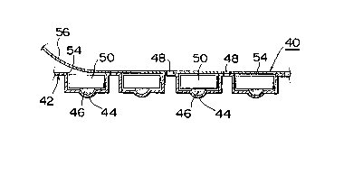
Fig. 3 shows another example of an electronic co~ponent
series 42 prepared in the method according to the embodiment
of the present invention. In this example, a carrier tape
42 has a plurality of concavities 54 at equal intervals
along the longitudinal direction of the carrier tape 42 to
form hollows for receiving chips 50 therein, and has a tiny
- 9
recess portion 44 formed at a bottom of each of the
concavities 54 in a manner to be swelled in ~he downward
direction from the bottom of the concavity 54, in each of
which recess portions 44 an adhesive 46 is received.
Through the adhesive 46, a chip 50 received within each
concavity 54 is held on the inner bottom surface of the
concavity 54. This example comprises an additional cover
tape 56 which is stuck onto an upper surface of the carrier
tape 42 to cover the respective concavities 54, but the
cover tape 56 may be omitted. In this example, feeding
perforations 48 are formed by, for example, punching
predetermined portions of the assembly of the carrier tape
42 and cover tape 56.
The adhesive 46 employed in the electronic component
series 40 shown in Figs. 1 and 2 is preferably formed of
po7ymeric material which is selected from the ~roup
consisting of silicone, acrylic resin and the mixture of
silicone and acrylic resin which has the property of
exhibiting adhesion upon being heated to about 80C.
Incidentally, some chips are provided with three leads
50a as shown in Fig. 4 or provided with leads 50a like crab
legs as shown in Fig. 5. ~hen such chips 50' having a lot
of leads as these are mounted on a printed circuit board, it
is desirable that temporary fixing of the chips 50' onto the
printed circuit board should be carried out in a manner to
cause the chips 50' to be bonded at a plurality points on
their bottom surfaces to the printed circuit board ~1ith
A
'34L~
- 10 --
adhesives. Accordingly, when such chips 50' are treated
in the method of the present invention, it is desirable
to construct an electronic component series 40 in a manner
such that a cluster of tiny recess portions (idential to
the portions 44 shown in Figs. 1 and 3) is formed at a
portion of a carrier tape on which each chip 50' is to be
arranged, adhesives are received in the respective clusters
of the recess portions, and the chips 50' are then located
on the carrier tape so as to be contacted with the adhesives
received in the respective clusters of the recess portions
so that they are held on the carrier tape through the
adhesives. When a chip 50' is removed from the
so-constructed electronic component series in the manner
as described hereinafter, the adhesives 46 are also removed
from the carrier tape in a state of adhering on the bottom
surface of the removed chip 50' as shown in Figs. 4 and
5. Thus, even when the chips 50' having leads 50a as shown
in Figs. 4 and 5 are treated, it is possible to accomplish
the firmly temporary fixing of the chips 50' on a printed
circuit board.
The electronic component series 40 of Figs. 1 and 3
constructed as stated above is spirally wound around a reel
(not shown). The reel having the electronic component
series 40 spirally wound therearound, when it is used, is
installed in an apparatus (not shown) for automatically
mounting chips on printed circuit boards. In the mounting
S~4
apparatus, any suitable feeding means, e.g., teeth Or a
feed wheel are engaged with the feeding perforations 48
Or the electronic component series 40 to cause the
electronic component series 40 to be drawn out from the
reel with rotation of the feed wheel, whereby each of chips
50 or 50' on the carrier tape 42 is forwarded to a position
at which each of chips 50 or 50' on the carrier tape 42
is to be removed from the carrier tape 42. Incidentally,
in cases where the electronic component series 40 shown
in Fig. 3 is used, the cover tape 56 is peeled from the
carrier tape 42 by any suitable means, e.g., a ta~eup drum,
during the electronic component series 40 is moved toward
the chip removing position.
Referring to Fig. 6, the manner of removing of chips
50 from the carrier tape 42 of the electronic component
series 40 shown in Fig. 1 will be described. In Fig. 6,
a reference numeral 300 designates a suction head which
is incorporated into an automatic chip mounting apparatus
(not shown) and which serves to remove the chips 50 one
by one from the electronic component series 40 by suction
to place them on a printed circuit board. The suction head
300 is connected to an air-absorbing source (not shown)
for sucking the chips 50 one by one from the electronic
component series 40. Further, the suction head 300 is
adapted to be moved vertically with respect to the
electronic component series 40 and a printed circuit board.
45&4
- 12 -
Furthermore, the suction head 300 is adapted to be moved
between a position X1 at which each of the chips 50 is to
be removed from the carrier tape 42 of the electronic
component series 40 and a position X2 at which each of
so-removed chips 50 is to be mounted held on a printed
circuit board, and is normally at a position right above
the chip removing position X1. The above-mentioned
movements of the suction head 300 are carried out by any
suitable means, e.g., reciprocating cylinder means.
Arranged at a position right below the chip removing
position X1 is an ejector pin 302 which is adapted to be
moved vertically with respect to the electronic component
series 40. The ejector pin 302 is normally at a downward
position. In Fig. 6A, the electronic component series 40
is drawn out from the unshown reel having the electronic
component series 40 wound therearound by the unshown feeding
means to be moved in the longitudinal direction, whereby
the foremost one of the chips 50 on the carrier tape 42
reaches the chip removing position X1. At this time, the
suction head 300 is moved downwardly to be contacted at
its lower end with the chip 50 and then holds it by suction
as shown in Fig. 6B. Thereafter, the suction head 300
having the chip 50 held thereby is moved upwardly in order
to remove the chip 50 from the carrier tape 42.
Simultaneously with the upward movement of the suction head
300, the ejector pin 302 is moved upwardly to push up a
1,'~3~S~4
recess portion 44 of the carrier tape 42 on which the chip
50 is held through an adhesive 46 received in the recess
portion 44. At this time, with the pushing motion of the
ejector pin 302, the recess portion 44 is reversed in a
manner such that the bottom portion of the recess portion
44 actively projects upwardly as shown in Fig. 6C, since
the carrier tape 42 is made of a flexible resin material
as described above. Thus, the chip 50 is easily removed
from the carrier tape 42 by the upward movement of the
suction head 300 as shown in Fig. 6D. Naturally, the
adhesive 46 is also removed, in a state of adhering on the
bottom surface of the chip 50, from -the carrier tape 50.
Thereafter, the suction head 300 having the chip 50 held
thereon by suction is moved to the chip mounting position
X2 to place the chip 50 on a printed circuit board 400 (Fig.
7), resulting in the chip 50 being temporarily bonded onto
the printed circuit board 400 through the adhesive 46 having
adhered on the bottom surface of the chip 50. Incidentally,
in cases where the adhesive 46 is formed of a polymeric
material as described above, the adhesive 46 having adhered
on the bottom surface of the chip 50 is subjected to a
heating treatment before the suction head 300 is moved
downwardly to cause the chip 50 to be placed on the printed
circuit board 400. The heating treatment may be carried
out using hot air ejected from a hot air ejection nozzle
304 as shown in Fig. 7. The heating treatment may be
- 14 -
carried out using, as the hot air, air heated to a
temperature of about 80 C, resulting in the adhesive 46
exhibiting adhesion. Thus, the chip 50 is temporarily
bonded on the printed circuit board 400, using the adhesion
of the heated adhesive 46. Also, the heating treatment
may be performed utilizing means for irradiating heat beam,
a heating oven or a heater.
Incidentally, in cases where a chip 50' shown in Figs.
4 and 5 is removed from the carrier tape 42 having chips
50' held thereon, a cluster of recess portions of the
carrier tape on which the chip 50' is held may be pushed
up, by a plurality of ejector pins corresponding in number
to the recess portions, in the above-mentioned manner.
The above-described procedure is repeated to
temporarily fix a predetermined number of chips on a printed
circuit board. Thereafter, the printed circuit board is
transferred to a station for soldering. In the soldering
step, the chips are practically fixed on the printed circuit
board by soldering external terminals of the chips to the
printed circuit board.
Thus, it will be noted that a method of mounting chips
on a printed circuit board according to the present
invention is capable of easily removing chips together with
adhesives from an electronic component series to temporarily
fix them on a printed circuit board with the adhesives
having adhered on the bottom surfaces of the removed chips.
- 15 -
While a preferred embodiment of the present invention
has been described with a certain degree of particularity
with reference to the drawings, obvious modifications and
variations are possible in the light of the above teachings.
It is therefore to be understood that within the scope of
the appended claims, the invention may be practiced
otherwise than as specifically described.