Sélection de la langue

Search

Sommaire du brevet 1294720 

Énoncé de désistement de responsabilité concernant l'information provenant de tiers

Une partie des informations de ce site Web a été fournie par des sources externes. Le gouvernement du Canada n'assume aucune responsabilité concernant la précision, l'actualité ou la fiabilité des informations fournies par les sources externes. Les utilisateurs qui désirent employer cette information devraient consulter directement la source des informations. Le contenu fourni par les sources externes n'est pas assujetti aux exigences sur les langues officielles, la protection des renseignements personnels et l'accessibilité.

Disponibilité de l'Abrégé et des Revendications

L'apparition de différences dans le texte et l'image des Revendications et de l'Abrégé dépend du moment auquel le document est publié. Les textes des Revendications et de l'Abrégé sont affichés :

  • lorsque la demande peut être examinée par le public;
  • lorsque le brevet est émis (délivrance).
(12) Brevet: (11) CA 1294720
(21) Numéro de la demande: 1294720
(54) Titre français: DISPOSITIF D'AFFICHAGE
(54) Titre anglais: DISPLAY DEVICE
Statut: Périmé et au-delà du délai pour l’annulation
Données bibliographiques
(51) Classification internationale des brevets (CIB):
  • G09G 03/36 (2006.01)
  • G09G 03/34 (2006.01)
  • H04N 03/12 (2006.01)
(72) Inventeurs :
  • GREEN, BERNARD JEFFREY (Royaume-Uni)
  • GREEN, IAN MACDONALD (Royaume-Uni)
  • GIBBONS, DAVID JOHN (Royaume-Uni)
  • ROWLEY, ANDREW TERENCE (Royaume-Uni)
(73) Titulaires :
  • CENTRAL RESEARCH LABORATORIES LIMITED
(71) Demandeurs :
  • CENTRAL RESEARCH LABORATORIES LIMITED (Royaume-Uni)
(74) Agent: SMART & BIGGAR LP
(74) Co-agent:
(45) Délivré: 1992-01-21
(22) Date de dépôt: 1987-09-21
Licence disponible: S.O.
Cédé au domaine public: S.O.
(25) Langue des documents déposés: Anglais

Traité de coopération en matière de brevets (PCT): Non

(30) Données de priorité de la demande:
Numéro de la demande Pays / territoire Date
8622711 (Royaume-Uni) 1986-09-20
8716162 (Royaume-Uni) 1987-07-09

Abrégés

Abrégé anglais


: 15 :
ABSTRACT OF THE DISCLOSURE
DISPLAY DEVICE
A colour-sequential display is formed by a matrix of
surface-stabilised bi-stable ferroelectric liquid crystal elements
each being separately settable by a matrix driver, to provide
brightness control of the display, the activation duration of the
sets of fluorescent tubes is variable, being dependent on the
binary significance of the brightness information for the relevant
colour in the input signal. Half of the frame time (T) is used
for the numerous setting operations on the matrix of elements and
half is used for the backlighting operations of the various
settings.

Revendications

Note : Les revendications sont présentées dans la langue officielle dans laquelle elles ont été soumises.


: 13 :
CLAIMS
1. A display device comprising a lattice of liquid crystal
display elements, each element selectively settable between two
states, one state allowing the transmission of light therethrough
and the other state not allowing the transmission of light
therethrough, means to effect setting of the lattice in accordance
with a portion of a signal for display, and means to control the
light output by the display device for a given setting of the
lattice, said control means including means to render the amount
of light passing through the lattice for a given setting
proportional to the binary significance of that portion of the
input signal.
2. A display device according to Claim 1, wherein the light
passage means comprises means to operate, for a given setting, a
light source at a light intensity proportional to the binary
significance of the portion of the signal for display at that
given setting.
3. A display device according to Claim 1, wherein in a colour
display, the light-passage means comprises means to operate three
light sources of different colour characteristics, such that the
intensity of each light source is proportional to the binary
significance of that portion of the signal for that setting.
4. A display device according to Claim 1, wherein the maximum
intensity for the three light sources is not the same.
5. A display device according to Claim 1, wherein the
light-passage means comprises means to generate a light source for
a time duration proportional to the binary significance of that
portion of the signal for that setting.
6. A display according to Claim 1 wherein, in a colour display,
the light-passage means comprises means to operate three light
sources of different colour characteristics, such that the
intensity of each light source is proportional to the binary
significance of that portion of the signal for that setting.
7. A display according to Claim 1, wherein the maximum time

: 14 :
duration for the three light sources is not the same.
8. A method of operating a display device comprising a lattice
of liquid crystal display elements, each element selectively
settable between two states, one state allowing the transmission
of light therethrough and the other state not allowing the
transmission of light therethrough, and method comprising setting
the lattice in accordance with a portion of a signal for display,
and controlling the light output by the display device for a given
setting of the lattice, said control stage including rendering the
amount of light passing through the lattice for a given setting
proportional to the binary significance of that portion of the
input signal.
9. A method according to Claim 8, comprising operating, for a
given setting, a light source at a light intensity.
10. A method according to Claim 8, comprising generating a light
source for a time duration proportional to the binary significance
of that portion of the signal for that setting.

Description

Note : Les descriptions sont présentées dans la langue officielle dans laquelle elles ont été soumises.


~r~
: 1 :
DISPLAY DEVIC~
The present invention relates to a display device
incorporating liquid crystal display elements.
British Patent Specification No~ 2172733A discloses a display
formed of a matrix of liquid crystal devices backlit by three
light sources which are switched on sequentially each for a time
duration corresponding to a third of the frame period The
intensity is controlled by using the liquid crystal elements in
the variable transmission mode.
. The present invention provides a display device comprising a
lattice of liquid crystal display elsments, each element
selectively settable between two states, one state allowing the
transmission of light therethrough and the other state not
allowing the transmission of light therethrough, means to effect
setting of the lattice in accordance with a portion of a signal
for display, and means to control the light output by the display
device for a given setting of the la~tice, said control means
including means to render the amount of liyht passing through the
lattice for a given setting proportional to the binary
significance of that portion of the input signal.
- 20 Preferably, the light passage means comprises means to
operate, for a given setting, a light source at a light intensity
proportional to the binary significance of the portion of the
signal for display at that given setting.
Advantageously, in a colour display, the light-passage means

?(:)
: 2
comprises means to operate three llght sources of different colour
characteristics, such that the intensity of each light source is
proportional to the binary significance of that portion of the
signal for that setting.
The maximum intensity for the three light sources need not be
the same; for example, if the three light source~ are such that
one emits green light, another blue light and the third red light,
then the green-emitting source may have a higher maximum intensity
than the red or the blue sources.
Additionally or alternatively the light-passage means
comprises means to generate a light source for a time duration
proportional to the binary significance of the brightness portion
of the input signal for that pixel. Por a colour display,
preferably the light-passage means comprises means to operate
lS three light sources of different colour characteristics, such that
the intensity of each light source is proportional to the binary
significance of that colour brightness for that pixel in the input
signal to the device. The maximum time duration for the three
light sources need not be the same.
Preferably, the signal for one picture comprises a sequence
of words (for example each of 8 bits), each one corresponding to
the display information for a display element in the lattice.
Thus the output means can operate such as to take out, from the
store, the first bit in each word and pass them sequentially to
the lattice; thereafter the output means can operate such as to
take out, from the store, the second bit in each word and pass
them sequentially to the la~tice. This operation can be repeated
until all the bits have been processed in this way.
As the bits in a given positlon (e.g. first) in the display
wo{d reach the drivers, they set each pixel to the corresponding
condition. Once the entire lattice has been set in accordance
with a given bit-position, the light-modulation means can be
activated to output light in accordance with the given
bit-position; thus, for example, if the given bit-position is the
first bit in the word and this is designated as the
most-significant bit, then the light output with the elements in

lZ~
` : 3
this condit1on is accordingly a substantial fraction of the total
output. The light output for the most-significant-bit setting
may be double that for the secondmost-significant-bit setting,
which is itself double that for the third most-significant-bit
setting, and so on. The light modulation means may have means to
regulate the intensity of the light output in accordance with the
given bit-position, and/or means to regulate the duration of light
output in accordance with the given bit-position.
Preferably the display device may have means to blank the
elements during setting of the elements for a given bit position.
For a colour display, preferably the display device has a
lattice formed of groups of three display elements, each of the
elements in a group producing a different colour and being set
separately. In an alternative arrangement, the lattice is formed
of single display elements, each of which is exposed to light of
the three colours sequentially, an element being re-set after each
exposure.
The present invention also provides a method of operating a
grey-scale display device having a lattice cf bi-stable display
elements, the method comprising:-
inputting a signal, representing the display information forone picture, to a store
outputting from the store a section of the display
information for one picture, the section consisting of
corresponding portions of display infor~ation for all the
bi-stable display elements;
using a plurality of drivers, each allocated to a row or
column of the lattice, to effect setting of each display element
to a condition in accordance with its respective portion of the
signal from the output meansS
producing a light output, once the elements are set,
modulated in accordance with the significance of the portion of
the video signal,
outputting from the store a second section of the display
information, the second section consisting of different
corresponding portions of display information for all the

: 4
bi-stable dLsplay elements, and effectlng the setting and
modulating operations for the second section~ and
repeating the outputting, setting and modulating operations
on any further corresponding portions.
Preferably, the signal comprises an 8-bit word for each
element, and the most-significant-bit of each word is first output
from the store for setting and display. Thereafter the
second-most-significant-bit of each word is output from the store
for setting and display, the total light output being half the
previous output. This sequence ~s repeated until the
least-significant bit has been displayed.
Preferably, modulation of the light output is achieved by
regulation of the light intensity and/or of the duration of light
output.
Preferably, each row and column of the lattice has a separate
driver. Alternatively, each column has a separate driver, and
some or all the rows have a common driver.
Preferably a display element comprises one or more
selectively-settable liquid crystal cells.
The present invention is applicable to many forms of
displays, for example to one in which the image is presented at a
surface of a liquid crystal panel backlit by fluorescent tubes, or
to one in which the image is projected onto a screen by means of a
liquid crystal panel positioned in the path of a light beam.
Also, the present invention is applicable to colour displays and
to black-and-white displays.
Furthermore, the present invention also embodies equipment
for the generation, and/or transmission, and/or reception, and/or
processing, of signals suited and/or designed for a display device
as herein defined.
Additionally or alternatively the light-passage means
comprises means to generate a light source for a time duration
proportional to the binary significance of the brightness portion
of the input signal for that pixel. For a rolour display,
preferably the light-passage means comprises means to operate
three llght sources of different colour characteristics~ such that

_ - : 5
the intensity of each light source is proportional to the blnary
significance of that colour brightness for that pixel in the input
signal to the device. The maximum time duration for the three
light sources need not be the same.
In order that the invention may more readily be understood, a
description is now given, by way of example only, reference being
made to the accompanying drawings in which:-
Pigure 1 is a block schematic cliagram of part of a display
device embodying the present inventionS
Figure 2 is a diagram of waveforms for use in a display
device embodying the present invention;
Pigure 3 is a diagram of waveforms for use in another
embodiment of display device;
Figure 4 is a diagram of a part of a further embodiment of
the present invention;
Figure 5 is a diagram of the sequence of waveforms in one
frame for a display device embodying the present invention;
Figure 6 is a block diagram of a display device embodying the
present invention; ~~
Figure 7 is another block diagram of a display device
embodying the present invention; and
Figure 8 shows a pixel arrangement for a display device
embodying the present invention.
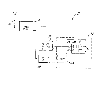
There is shown in Figure 1 part of a colour-sequential
display 1 formed by a matrix of surface-stabilised bi-stable
ferroelectric liquid crystal elements 2~ Each element 2 is
separately settable, by the output of appropriate signals from
- matrix driver 3 along column conductor lines 4 and row conductor
lines 5, between two states, in one of which light can pass
through the element and in the other of which light is prevented
from passing therethrough.
Display 1 has three sets (6, 7 and 8) of fluorescent tubes,
each set providing uniform backlighting of the matrix in a
respective colour (green, red, and blue) used to produce a colour
display.
In order to avoid any problems of top-bottom shading, all the

6 ~2~7~
elements 2 forming the matrix are set to their relevant state
(i.e. light-transmitting or light-blocking) in each field before a
set of fluorescent tubes is activated.
In order to provide brightness control of the display, the
activation duration of the sets of fluorescent tubes is variable,
being dependent on the binary significance of the brightness
information for the relevant colour in the input signal7 Half of
the frame time (T) is used for the numerous setting operations on
the matrix of elements and half is used for the backlighting
operations of the various settings. The setting and backlighting
operations in respect of the green light constitute half the fra~e
time, while those for each of the red and blue light constitute
quarter the frame time. This display utilises an eight
bit-encoded video signal consisting of four bits dedicated to the
green light information, and two bits dedicated to each of the red
and blue light information.
More specifically, in order to display the green light
information in one frame, there is a sequence of four consecutive
_ _ writing operations each separated by a green backlighting pulse of
predetermined duration and amplitude. The writing of a stable
bi-level pattern is achieved, while all the lights are off, by
addressing the matrix via lines 4 and 5 according to the
significance of the respective bit in the input video signal.
For example, a bi-level pattern corresponding to the
most-significant-bit is written over the entire matrix and, once
completed, tube set 6 is turned on with an intensity 8Ig for a
time period T/16, where Ig is a reference light intensity for
the green image. Tube set 6 is then turned off for T/16, during
which the matrix is overwritten to form a pattern appropriate to
the next most-significant-bit, this taking T/16; once completed,
tube set 6 is turned on at an intensity 419 for T/16. Then the
light is pulsed off again for T/16, and the matrix is overwritten
to produce a pattern corresponding to the next most-significant-
bits for the green image, after which tube set 6 is turned on for
T/16 at intensity 2Ig. The overwriting and exposure sequence
is repeated again, for a lighting intensity of Igl whereupon

7~
: 7
display of the green image is completed.
To achieve display of the red image, a simllar routine is
followed but this time only two patterns are over~ritten and
exposed, the first pattern at an intensity of 2Ir and the second
at an intensity of Ir. Each pattern is written in a time period
of T/16, with tube set 7 off. Por the blue image, this routine
of only two patterns is repeated, at intensities 2Ib and Ib.
Figure 2 shows the relevant waveforms used to produce a display
with these routines.
In an alternative form, the duration of exposure of the
various patterns differs, while the intensity of the light ~ources
remains the same for all the patterns overwritten Thus, to
display the green light information, there are four
overwriting/exposure operations each having a common writing
duration, but having differing exposure durations of 8tg, 4tg,
2tg and tg. Likewise each of the routines for producing the
red and blue displays has two overwriting/exposure operations
having differing exposure durations of 2tr and tr, or 2tb
and tb respectively.
As the display 1 conforms to the PAL system standards, each
frame must consist of 575 active lines per 40 msec which must be
displayed every 20 msec to ensure a flicker-free image. In each
20 msec period, eight fields corresponding to each grey level and
colour need to be written, so that the total ~riting time in
4.3N ~sec per line, where N is the number of subdivisions of the
display area that can be addressed in parallel. Such parallel
addressing can be achieved in a number of ways, one of which is to
utilise the arrangement of light gates and conductors a^q shown in
Figure 4, whereby each column is made up of four sub-electrodes A,
B, C and D. In this way, by doubling the number of light gates
per line conductor and doubling the number of column conductors
it is possible to switch four lines simultaneously. ThUs, by
addressing 144 lines sequenti~lly downwards from ~he top while
simultaneously addressing 144 lines sequentially upwards from the
bottom, a total of 576 lines are addressed in the time taken to
scan 144 lines. In this instance, ~ = 4 and so, if all the
~,

~2~P~72![)
: 8
fields are to be written in 20ms, the time available for writing
is 17 IJsec per line.
In a modification, both the duration of exposure and the
intensity of the light sources can be made to be variable.
The three sets 6, 7, 8 of fluorescent tubes are contained in
a housing designed to provide a uniform flux of each colour into
the display. The sets of tubes usecl in the backlight are low
pressure mercury~rare gas (LPMV) discharge lamps coated on the
inside wall with a phosphor, chosen to have appropriate spectral
distribution, rise and decay time characteristics. ~he lamps are
run off a high frequency supply ( ~ 10 kHz) which ls switched
sequentially between the three lamps using non-rectifying
thyristor switchlng elements. The on-time of the lamp may be
made variable, consistent with the transmissive mode window of the
display to provide colour balance and overall brightness
adjustment.
Figure 5 shows a sequence of addressing signals appropriate
to produce an 8-colour display suitable for most alphagraphics and
capable of three times the resolution of a microdot colour
display, since it requires only one cell per picture element.
With a suitable liquid crystal display device it would be possible
to arrange ~or temporal and/or spatial modulation of each gate to
provide halftoning.
The use of a bi-stable ferroelectric liquid crystal display
in the manner described above enables the possibility of providing
for each pixel, six colours together with black and white.
The colour-sequential technique of addressing mentioned above
requires the tubes to run at frequencies greater than about 65 ~z
in order to provide flicker-free displays. There is about 5 msec
available for each frame of information on an individual colour,
during which period the information has to be written on the
display and illuminated. Such time restraints require the
phosphor to be used to have specific characteristics including a
narrow band emission at an appropriate wavelength and a decay time
(i.e. time to fall to 10~ of maximum or operational output) of
less than 1 msec. Cheap wide band (light transmission) filters

~lZ~72~
, g
are used to filter out the mercury spectral lines from the light
output.
Resistive ballasts are used if square light pulses are
required to illuminate the display, and also because they do not
introduce any delays into the circuit. By making part of the
ballast resistance variable, the overall screen brightness and
colour can be simply adjusted. The pulse shape of the light
output can be altered by appropriate choice of ballast co~ponents,
for example, using reactive components. The possibility of
shaping the light output pulses allows the lines of display to be
switched whilst the lamps are on.
The sequence of illuminating the sets of tubes can be
important to the overall performance, and image-quality, of the
display. Thus Eor example the illumination seguence of red light
sources, then green light sources, then blue light sources can
substantially affect the colour performance as compared to the
sequence of red, then blue, then green sources.
The colour of the 6 available colours of the display can be
_ altered by changing the phase of the lamp pulse with respect to
~20 the LCD drivers. In effect, this moves a window across the light
output.
The colour of each individual pixel can be adjusted to give
more than the 6 colours previously mentioned by a similar
technique to that used to give control of the brightness of each
individual pixel (greyscale).
The television receiver 31 of Figure 6 has a liquid crystal
display 32 formed of a lattice of display elements 33 made from
liguid crystal material, each ele~uent being individually
actuable. The lattice of elemenrs 33 is backlit by a number of
fluorescent tubes 34 whose light intensity and duration of
operation can be controlled.
The video signal for input to television receiver has a 70HZ
scan rate providing a scan period of 14mS, and includes in each
picture of display information an 8-bit word for each display
element, a word beginning with the most-significant-bit and ending
with the least--significant-bit. When this signal is input to

721~
receiver 31 via its aerial 35, one picture of display information
passes to a frame store 36.
In the processing for the display of the most-significant-
bits of the word, frame store 36 outputs the first bit of each
word and sends the bits to a control unit 37 for an array of
drivers 38, one being assigned to each row and column of the
lattice. The driver array sets each element to the condition (on
or off) appropriate to its most-significant-bit. Once the array
of drivers 38 has set all the elements lwhich takes less than
lmS), driver control unit 37 instructs light switch unit 39 which
checks the relevant bit-position (in this case the
most-significant-bit) and then activates the fluorescent tubes 34
for a time duration of 3mS and at an intensity to provide an
appropriate output.
When the required output has been achieved then the light
switch unit 39 de-activates the tubes 34 ~nd instructs frame store
36 which proceeds to output the secondmost-significant bits to
driver control unit 37 thereby to set all the elements for this
bit-position. On this occasion, light switah unit 39 actLva~es ~-
the tubes half as long as before (namely 1.5mS) at the same
intensity to provide only half the output as that for the
most-significant bits. This routine is repeated for all eight
bits of the words, the light output being halved each time. Once
the least significant bit has been displayed (the light output
time duration being 25 S), the store 36 is emptied and the next
picture of display information is input and the processing
described above is repeated.
Figure 7 is a block diagram of a system 40 for displaying
off-air video pictures on a bistable display, such as a
ferroelectric liquid crystal display panel. Video information is
received at aerial 41 and demodulated by the receiver 42; it is
then digitized (four bits per pixel~ and held in the digital frame
store 43.
To display one video frame, firstly the data is split in~o
four streams (one for each bit) and compressed by shift registers
44 so each byte contains data for 8 pixels. The data is then

~2'39~72~
loaded into four buffer RAMs 45, so each RAM now contains one
frame of video information 1 bit deep. Accesslng of the RAMS 45
and the frame store is done under control of the address generator
46.
~or the sequential greyscale processing the data must be sent
to the display one bit at a time, i.e. firstly all the data from
RAM O is sent to the display (the least significant bit), then
followed in turn by each of the other 3 RAMs. AlSo, in order to
write data to the light crystal display panel each line of data
mmust be presented in a manner determined by the multiplexing
scheme; this processing is performed by the data preparation
block 47. Data is now in a form in which it can be sent to the
display panel under control of the multiplex controller block 48,
each line of data being latched into the column drive chips 49
while rows are strobed by the row drive chips 50. This results
in the data being latched into the display. After a full screen
of data has been written, the backlight is flashed for a length of
time corresponding to the significance of the bit being ~`
- displayed. This is done by the lamp drive circuit 50 under _
control of the multiplex controller 48.
The sequence of events which results in a full picture with
sixteen grey levels being displayed, is as follows:-
1. Load frame store 43;
2. Load buffer RAMs 45, one significant bit to each;
3. Load data from buffer RA~ O line by line into data
preparation unit 47;
4. Load data from buffer RAM 1 line by line into data
preparation unit 47;
5. Load data from buffer RAM 2 line by line into data
preparation unit 47;
6. Load data from buffer RAM 3 line by line into data
preparation unit 47;
7. Multiplex controller 48 sends data from data preparation unit
47 to column drive chips 49 and controls row drive chips 50;
8. When data from RAM O has been latched into the display (i.e.
when the least significant bit for the frame is being presented),

:~2~
: 12
the multiplex controller 49 signals the lamp drive to flash for a
period of time A mS:
9. Data from RAM 1 is now latched and the backlight Plashed for
2A mS;
10. Data from RAM 2 is now latched 2nd the backlight flashed for
4A mS;
11. Data from ~AM 3 is now latched and the backlight flashed for
8A mS;
12. The picture has now been displayed.
Assuming a frame time of ~0 mS, then if it takes T mS to set up
the display 4T + 15A = ~OmS.
Figure 8 shows an arrangement of metallisation patterns for a
liquid crystal display panel to achieve a two-bit greyscale, for
use additionally or alternatively to the greyscale processing of
Figures 6 and 7. On the substrate 30 having the column
electrodes, the ITO metallisation patterns are such that each
pixel has two sections 61, 62 which can be separately driven from
appropriate drive chips tnot shown) on flexible pcb boards 63 and
64 via lines 65 and 66 respectively. For each pixel, section 61
corresponds to the least-signific~nt-bit, and section 62 to the
most-significant-bit. The row electrodes are formed by ITO
metallisation strips 67 on substrate 68, which can be strobed by
row drive chips tnot shown) on flexible pcb 69 via lines 70. In
Figure 8, on the left hand side the substrate has been omitted as
indicated by the broken-chain line yet the column metallisation is
shown overlying the row metallisation, for the purpose of
simplicity.

Dessin représentatif
Une figure unique qui représente un dessin illustrant l'invention.
États administratifs

2024-08-01 : Dans le cadre de la transition vers les Brevets de nouvelle génération (BNG), la base de données sur les brevets canadiens (BDBC) contient désormais un Historique d'événement plus détaillé, qui reproduit le Journal des événements de notre nouvelle solution interne.

Veuillez noter que les événements débutant par « Inactive : » se réfèrent à des événements qui ne sont plus utilisés dans notre nouvelle solution interne.

Pour une meilleure compréhension de l'état de la demande ou brevet qui figure sur cette page, la rubrique Mise en garde , et les descriptions de Brevet , Historique d'événement , Taxes périodiques et Historique des paiements devraient être consultées.

Historique d'événement

Description Date
Inactive : Renversement de l'état périmé 2012-12-05
Le délai pour l'annulation est expiré 2009-01-21
Lettre envoyée 2008-01-21
Inactive : CIB de MCD 2006-03-11
Accordé par délivrance 1992-01-21

Historique d'abandonnement

Il n'y a pas d'historique d'abandonnement

Titulaires au dossier

Les titulaires actuels et antérieures au dossier sont affichés en ordre alphabétique.

Titulaires actuels au dossier
CENTRAL RESEARCH LABORATORIES LIMITED
Titulaires antérieures au dossier
ANDREW TERENCE ROWLEY
BERNARD JEFFREY GREEN
DAVID JOHN GIBBONS
IAN MACDONALD GREEN
Les propriétaires antérieurs qui ne figurent pas dans la liste des « Propriétaires au dossier » apparaîtront dans d'autres documents au dossier.
Documents

Pour visionner les fichiers sélectionnés, entrer le code reCAPTCHA :


Pour visualiser une image, cliquer sur un lien dans la colonne description du document. Pour télécharger l'image (les images), cliquer l'une ou plusieurs cases à cocher dans la première colonne et ensuite cliquer sur le bouton "Télécharger sélection en format PDF (archive Zip)" ou le bouton "Télécharger sélection (en un fichier PDF fusionné)".

Liste des documents de brevet publiés et non publiés sur la BDBC .

Si vous avez des difficultés à accéder au contenu, veuillez communiquer avec le Centre de services à la clientèle au 1-866-997-1936, ou envoyer un courriel au Centre de service à la clientèle de l'OPIC.


Description du
Document 
Date
(aaaa-mm-jj) 
Nombre de pages   Taille de l'image (Ko) 
Abrégé 1993-10-25 1 26
Revendications 1993-10-25 2 58
Dessins 1993-10-25 6 124
Description 1993-10-25 12 448
Dessin représentatif 2002-04-09 1 5
Courtoisie - Certificat d'enregistrement (document(s) connexe(s)) 1998-07-19 1 140
Avis concernant la taxe de maintien 2008-03-02 1 174
Taxes 2001-10-14 1 29
Taxes 2000-11-28 1 32
Taxes 1998-11-22 1 31
Taxes 2002-10-10 1 35
Taxes 1997-10-20 1 28
Taxes 1999-10-26 1 27
Taxes 2004-12-21 1 27
Taxes 2006-01-17 1 23
Taxes 1996-10-20 1 41
Taxes 1995-10-12 1 52
Taxes 1994-10-10 1 34
Taxes 1993-01-21 1 26