Note : Les descriptions sont présentées dans la langue officielle dans laquelle elles ont été soumises.
~2~53~3
SPREAD SPECTRUM POWh'R LINE COMM~JNICATIONS
BACKGROUND OF THE INVENTION
~ his invention relates in general to power line
communications. More specifically, it provides various
improvements for systems wherein a central station "master"
~onitors and communicates with a plurality of ~slave" units using
a power line as a transmission line for communications.
A security system is one example of a system that
requires centralized monitoring of slave units by a master.
Various sensors such as infrared intrusion, window - glass damage
and fire detection sensors are installed in target areas to be
protected. These sensors are connected to a supervisory unit
through ind~vidual transmitters and circuits respectively for
centralized monitoring.
A problem of conventional "wired" master/s~ave systems
is that, as the number o~ slave units and monitoring range
increase, the amount of wiring required becomes excessive. A
powe~ line providing power to the various slave units can be used
for communications, but there are many factors which make it
difficult to communicate reliably over a power line. ~or
2Q example, it is usually necessary to provide an arrangement for
the prevention of signal line disconnections and quick detection
of such disconnection faults.
Various schemes have been proposed to establish and
maintain communications over a commercial power line. A
transmission line generally utilizes single side band modulation
for data signals, whereas a frequency or phase modulation is used
for a distribution line.
A power line is not designed for signal transmission.
It is electrically noisy, has a wide range of impedances, and its
transmission characteristics fluctuate with line load. As a
consequence, reliable signal transmission and particularly high
1~5393
1 speed dat~ transmission have not been possible using conventional
techniques.
There has been study undertaken in the applications of
so called "spread spectrum" communications. The Journals of the
Institute of Electronic and Communications Engineers of Japan;
Sept/82, p 965 & Oct/82, p 1063 discloses the principles of and
comments on the applications spread spectrum technology.
Spread spectrum communications system relies on so-
called Pseudo-Noise (PN) diffusion or direct diffusion. A
narrow-band data signal is transmitted over a wide-band
transmission by diffusing the spectrum thereof using an M
~eqlential code as a spurious noise signal. Even if the
transmission characteristics of the transmission medium have a
plucality Gf zero points resulting from the line load, a
transmitted signal not be substantially affected thereby. Even
if narrow-band noise is blended with a transmitted data signal,
the S/N ratio can be improved using correlation at the receiver.
~ owever, the application of spread spectrum technology
to power line communication systems permitting one master unit to
similtaneously monitor a plurality of slave units still poses
problems. For example, if multiple slave units simultaneously
sen~ data signals to the master unit, the data signals overlap
and can not be discriminated from one another. To prevent the
sla~e units from sending the data signals to the master unit
simultaneously, polling schemes have been used. In effect, the
master takes turns looking at each slave successively to see if a
given slave has a message to send to the master. Such systems
require additional hardware, such as a CPU to control the
polling, and are expensive.
-- 2 --
3~3
1 In one of its aspects, the present invention providec
a spread spectrum power line carrier frequency communications
method comprising the steps of:
connecting a plurality of slave units and one master
unit to a common power line,
checking by a slave unit for the presence of a signal
transmitted by any other slave unit on said power line when it
needs to transmit a signal,
in the event that a checking slave unit does not
detect a signal transmitted by another slave unit, transmitting
a data signal using spread spectrum modulation with maximum
length sequence, but in the event that a checking slave unit
detects a signal transmitted by another slave unit, not
transmitting,
and receiving via said power line by said master unit
said data signal and demodulating it.
- 2a -
393
BRIEF DESCRIPTION OF THE DRAWINGS
1 FIGUR~ 1 is a block diagram of a spectrum scattering
power line carrier fre~uency communication system.
FIGURE 2 is a circuit diagram of the transmitter and
receiver M-series code generators shown in FIGURE 1.
s PIGURE 3 shows various operational waveforms (a) to (f)
at. various portions for explaining the operations the circuit
shown in FIGURE 2.
FIGURE 4 is a block diagram of a transmitter (slave)
unit for a spread spectrum communication arrangement according to
the invention wherein slave unit transmissions are prevented from
overlapping.
FIGURE 5 is a schematic diagram of the M sequential code
generating circuits which are shown as blocks 8 and 9 in FIGURE
4.
FIGURE 6 is a block diagram of a receiver (master) unit
that operates with slave units of the type shown in FIGURE 4.
FIGURE 7 is a schematic diagram of the first M
sequential code generator circuit 32 and the phase-shift control
circuit 38 shown as blocks in FIGURE 6.
FIGURE 8 and FIGURE 9 are flow charts showing the
operation of the master and slave units shown in FIGURE 4 and
FIGURE 6.
FIGURE 10 is a block diagram of a line lock
communication arrangement for power line communication according
to the invention.
FIGURE 11 is a schematic diagram of the line lock clock
generator and the transmitter M-series code generator shown as
blocks in FIGURE 10.
FIGURE 12 shows various operational waveforms (a) to (j)
explaining the operation the arrangement shown in FIGURE 11.
~C - 3 -
1~3~3~33
1 FIGURE 13 is a block diagram of a spread spectrum power
line carrier fre~uency communications arrangement using a gold
code generator according to the present invention.
FIGURE 14 is a schematic diagram of the gold code
generator shown as a block in FIGURE 13.
FIGURE 15 is a circuit diagram of the gold code selector
shown in FIGURE 13.
FIGURES 16(a)-(f) show waveforms illustrating the
operation of the FIGURE 13 system.
FIGURE 17 is a block diagram of another gold code
embodiment of a master unit according to the present invention.
FIGURE 18 is a schematic diagram of the gold code
selector of FIGURE 17.
FIGURE 19 is a block diagram of another embodiment of a
line lock spread spectrum communication arrangement according to
the present invention.
FIGURE 20 is a diagram showing an example of the
spectrum distribution of the transmission output produced from
the transmitter of FIGURE 19; and
PIGURE 2L is a diagram showing an example of the used
frequency band of an interphone utilizi.ng the power line carrier
frequency communication.
FIGURE 22 is a block diagram of another embodiment o~ a
spread spectrum arrangement for power ~ine transmission according
to the invention.
FIGURE 23 is a block diagram showing one example of a
receiving signal level control circuit in FIGURE 22.
FIGURE 24 is a waveform diagram showing the operation of
the receiving signal level control circuit shown in FIGURE 23.
FIGURE 25 is a block diagram of another embodiment of
the communication arrangement according to this invention;
- 4 -
lZ~393 . I
1 FIGURE 26 is a schematic diagram showing one
suitable circuit configuration of M-series code generating
circuit 502 shown in FIGURE 25.
FIGURE 27 is a graphical representation indicating
the spectra of a main lope provided when a band used is
switched.
FIGURES 2~ and 29 are graphical representations
indicating transmission characteristic curves of power
lines.
FIGURE 30 is a block diagram of a spread spectrum
power line carrier communication arrangement according to
the present invention.
FIGURE 31 is a circuit diagram of the A.C.
synchronizing clock generator circuit of FIGURE 32.
FIGURE 32 is a circuit diagram of the gold code
generator circuit and address setting unit of FIGURE 32.
The present invention provides various
improvements in power line communications. Using the
arrangements of the prssent invention, it is possible to
achieve reliable and inexpensive centralized monitoring of a
plurality of slave units by one master unit through a power
line without the need to use a CPU (Central Processing Unit)
for polling.
According to one aspect of the invention (See
FIGURE 4 - FIGURE 9), signals transmlttsd by a plurality of
slave units to a master unit are prevented from overlapping
one another. A slave unit having a message to transmit
first checks for the presence of any spread spectrum
modulated signal on the power line. If there is already a
spread spectrum signal on the line, it does not transmit.
However, if the line is judged to be free by the absence of
any spread spectrum signal, it transmits its data message
using spread spectrum modulation.
Each slave unit generates a first M sequential
transmission code for use in spread spectrum modulating a
data signal and a second M sequential transmission code
having the
-- 5 --
;3~3
1 same code pattern as that of the first M sequential code
I transmission code. The second M sequential transmission code is
added to the spread spectrum signal modulated by the first M
sequential transmission code only when the data signal is
produced. This "combined" signal is transmitted onto the power
line. A slave unit transmitting a signal is discriminated from
the others by setting the phase difference inherent in each slave
unit between the M sequential transmission codes.
~he phase of the second M sequential transmission code
produced by each slave unit is successively shifted from one unit
to the next. Whether or not any other slave unit is transmitting
a signal is determined by obtaining the correlation between the
signals received through the power line.
The master unit produces a first M sequential reception
code for use in demodulating a received spread spectrum modulated
signal, the first M sequential reception code having the same
code pattern as that of the first M sequential transmission code,
and a second M sequential reception code for use in correlating
with the first M sequential transmission code, the second M
sequential reception code having the same code pattern as that of
the first M sequential transmission code. The codes are
synchronized by successively varying the phase of the clock pulse
providing a basis for the generation of the first and second M
sequential reception codes on the basis of a period greater than
the period wherein the second M sequential reception code is
produced until the correlation of the second M sequential
reception code to the second M sequential transmission code
received from the slave unit is obtained.
-- 6 --
12~3~3
1 The received spread spectrum modulated signal is
multiplicatively demodulated while only the phase of the first M
seq~ential reception code is shifted at least in the period
wherein the code is produced when the correlation between the
second M sequential transmission code and the second M seguential
reception code is obtained. Phase shifting is stopped when the
dem~dulated signal is obtained so as to extract the receiving
signal and the slave unit transmitting a signal is discriminated
frotl the others according to the difference in phase between the
first and second M sequential reception codes.
Transmission-to reception phase synchronization is
secured by locking a cloc~ pulse generator circuit installed in
each of the slave units and the master unit to a power supply for
supplying A.C. through the power line.
Slave units are prevented from transmitting signals
simultaneously. Each slave unit is allowed to spread spectrum
modulate with M se~uential codes and transmit the thus modulated
signal only after confirming the absence of any spread spectrum
modulated signal flowing through the power line.
Each slave unit is transmits data with the first and
second M sequential transmission codes produced for spread
spectrum modulating in such a state that each code has the phase
difference inherent in each slave unit and transmits the
combination of the second M sequential transmission code and the
spread spectrum modulated signal added thereto so that any slave
unit transmitting a signal may readily be discriminated from the
others by obtaining the difference in phase between the first M
sequential reception code for use in demodulating the receiving
spread spectrum modulated signal on the part of the master unit
and the second M sequential reception code for obtaining t~e
35~3~3
1 correlation thereof to the second M sequential transmission code
contained in the receiving signal.
Each slave unit is, if a data signal to be transmitted
is produced, caused to transmit the combination of the spread
spectrum modulated signal obtained by multiplicatively modulating
the data signal with the first M sequential transmission code and
the second M Sequential transmission code to the power line. In
consequence, each slave unit is readily capable of noticing any
other slave unit, if any, transmitting a signal by successively
shifting the phase of the second M sequential transmission code
to find whether or not the correlation of the code to the signal
supplied through the power line is obtainable.
The clock pulse generator circuit in each of the slave
ancl master units arranged to produce the clock pulse whose phase
is locked to the A.C. power line frequency to ensure the
acquisition of the correlation of the second M se~uential
rec:eption code produced with the clock pulse as a basis to the
second M sequential transmission code received and the
multiplicative demodulation of the receiving spread spectrum
modulated signal by means of the first M sequential reception
code.
Another aspect of the invention relates to a line lock
communication arrangement using a power source for
synchronization of operations between a transmitter and a
receiver (See FIGURE 10 - FIGURE 12). FIGURES 1 - 3 provide some
background for understanding the line lock aspect of the
invention.
- 8 -
~Z~53~3
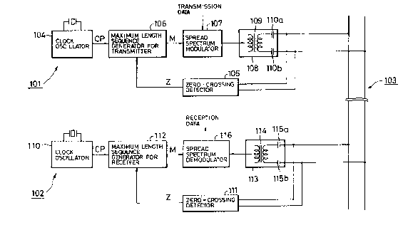
1 FIGURE 1 is a block diagram showing one example of an
application of the spread spectrum technique to power line
communication. Data is modulated using a pseudo-noise (PN)
signal scattering or direct scattering, and particularly, an M-
series code is used as the Pseudo Noise (PN) signal. The M-
series code is the longest one of linear code series generated by
both a multistage shift register and a feedback circuit and
established so that instantaneous values every period are
distributed in the sate of quasi-noise. A transmitter 101 and a
receiver 102 are coupled to each other via a power line power
lin~ 103. A clock oscillator 104 generates a clock pulse CP
having a frequency of 250 KHz. A zero-crossing detector 105
generates a zero-crossing detecti.on Z every time a zero-crossing
point of the A.C. power carried by power line power line 103 is
detected. An M-series code generator 106 generates an M-series
code as a PN s1gnal. rn the FIGURE 2 arrangement, an M-series
code generator includes a three-stage shift reglster 106a and an
exclusive OR gate 106b for exclusively ORing the output signals
of the second and third stages of the shift register to thereby
feedback the resulting signal to the input terminal. The M-
series code generator generates from the last stage thereof an M-
series code having a maximum code length of 2n-1 (wherein n is
the number of shifting stages). The M-series code generator is
arranged such that upon reception of a zero-crossing detection
signal Z supplied from 105, all of flip-flop circuits FFl to FF3
constituting the respective stages of three-stage shift register
106a are reset to "1".
A spread spectrum modulator 107 product- modulates
~exclusively ORing) the transmission data and the M- series
code. This converts the data signal to be transmitted to a
spread spectrum modulated signal. A coupler 108 including a
y _ g _
5393
1 transformer 109, a capacitor llOa and a capacitor llOb, receives
the modulated signal supplied from spread spectrum modulator 107
through a filter (not shown) for eliminating low frequency
components and transfers the modulated signal to power line 103.
In receiver 102, a clock oscillator 110 generates a
clock pulse CP the same as that of 104 in transmitter 101. A
zero- crossing detect~or 111 for generating a zero-crossing
detection signal Z whenever a zero-crossing point of the A.C.
supply supplied through power line 103 is detected. An M-series
code generator 112 in receiver 102 has the same construction as
M-series code generator. A coupler 113 "extracts" the spread
spectrum modulated signal from power line 103. Coupler 113 is
con~tituted by a transformer 114 and capacitors 115a and llSb. A
spread spectrum demodulator 116 multiplies the modulated signal
supplied from coupler 113 through a receiver amplifier as well as
a low- frequency cut filter (both not-shown) with the M-series
code supplied from M-series code generator 112, so as to make a
cor~elation detect~on of the data signal.
Upon turning the power switch on, clock oscillator 104
and clock oscillator 110 respectively pro~ided in transmitter 101
and receiver 102 generate clock pulses CP having the same
period. Zero-crossing detector 105 and zero crossing detector
111 provided in transmitter 101 and receiver 102 respectively,
generated zero-crossing detection signals Z indicating each zero-
crossing point of the A.C. supply flowing in power line 103, thezero-crossing detection signals Z generated from both zero-
crossing detector 105 and zero crossing detector 111 being in
synchronism with each other.
!~ When the zero-crossing detection signal Z is generated
from zero-crossing detector 105 at the point in time tl of FIGURE
3~f), all the respective outputs of the flip-flop circuits FFl to
FF3 a.e rest to "1" because three-stage shift register 106a
receives the zero-crossing detection signal Z as a reset
X
- 10 --
~'Z~393
1 signal. Accordingly, the output signal of exclusive OR gate 106b
becomes "0" as shown in FIGURE 3(d). Next, when the clock pulse
CP rises at time t2 of ~IGURE 3le), three-stage shift register
106a reads- in the output signal of exclusive O~ gate 106b and
shifts so that the outputs of the flip-flop circuits F~l to FF3
become "0", "1" and "1", respectively. When the olock pulse
rises at time t3 of FIGURE 3(e), the output of exclusive OR g2te
106b is maintained "0" and three-stage shift register 106a
receives the "0" output signal of exclusive OR gate 106b to caus~
shifting so that the output signals of the flip-flop circuits FFl
to FF3 become "0", "0" and "1", respectively. Being arranged to
receive the output signals of the flip-1Op circuits FF2 and FF3
as its input signals, exclusive OR gate 106b produces a "1"
signals as shown in FIGURE 3(d) if the output signals of the
flip-flop circuits FF2 and FF3 do not accord with each other.
The output signal of exclusive OR gate 106b is coupled to three-
s~age shift register 106a at the leading edge of a next clock
pulse CP. By repetition of such a procedure in order, an M-
series code having a yeriod Tl between the'points in time t2 and
t9 as shown in FIGURE 3(c) is obtained. Because the M-series
code is generated in accordance with reset processlng based on
the zero-crossing detection signal Z, the M-series code is in
synchronism with the A.C. power in power line 103.
The M-series code generated in synchronism with the A.C.
supply is subject to product-modulation with the transmission
data synchronized with the high-frequency clock pulse CP in the
spread spectrum modulator 107 so that narrow band transmission
signal is transmitted as a modulated signal in which the narrow
band transmission data are spectrum-scattered uniformly over a
3~ wide band. After low-frequency components are removed by a
filter (not-shown), the modulated signal is amplified to a
predetermined level by the transmitter amplifier and supplied to
power line 103 via coupler 10~.
,~
-- 1 1 --
12~3~3
l In receiver 102, M-series code ~enerator 112 generates
an M- series code the same as that ~f M-series code generator, on
the basis of the clock pulse CP provided by clock oscillator
110. 8ecause M-series code generator 112 is arranged to be reset
by the output signal Z of zero crossing detector 111 for
detecting a zero-crossing point of the A.C. supply flowing in
power line 103, the generated M-series code is synchronized with
the A.C. supply, that is, synchronized with the M-series code
generated by M- series code generator. Coupler 113 receives the
modulated signal generated by transmitter 101 from power line
103. The received modulated signal is amplified by a receiver
amplifier (not shown), and low-frequency components thereof are
removed by a filter. Then, the modulated signal is supplied to
the spread spectrum demodulator 116. The spread spectrum
demodulator 116 multiplies the M-series code supplied from M-
series code generator 112 with the received modulated signal
whiCh has been transmitted in the spectrum-scattered state, so
that reception data is isolated.
In the FIGURE 1 spread spectrum communication
arrangement, the respective transmitter and receiver M-series
code generators generate respective M-series codes on the basis
of the zero-crossing point of the A.C. supply flowing in the
power line to synchronize the M-series codes with each other.
~owever, the arrangement has a limitation.
When the frequency of the clock pulse is selected to be
250 KHz, the one chip width of the M-series code is l/250 = 4 ~
sec. In general, the phase difference between the respective M-
series codes used for modulation and demodulation in the
transmitter and receiver must be within (~/-) 0.5 chip for normal
communication. However, when the zero-crossing detector detects
a zero-crossing point, the timing of zero-crossing detection may
be shifted by about lO ~ sec, because of the characteristics of
the detector, and accordingly, the generated M-series code has a
X
- 12 -
1 phase shift by about 10 ~ sec to thereby make it impossible to
carry out normal communication. Further, because the respective
clock pulses generated in the transmitter and receiver are not
synchronized with each other, there may be a phase difference
between them of one clock period at the maximum, so that the
respective M-series codes are shifted in phase from each other by
(~/-) 1 chip to make it impossible to carry out normal
communication. Furthermore, in the case where an M-series code
is generated in synchronism with a zero-crossing point, the
operation of generating the M-series code is force reset and
stopped upon the detection of a zero-crossing point, because of
discord in period between the M-series code and the A.C. supply,
so that it becomes impossible to carry out normal communication
in the vicinity of a portion of the period of the M-series code
where a zero-crossing detection point is included. In addition,
for example, in the case where the transmitter is disposed
relatively far from the receiver, a phase difference in the A.C.
supply between the transmitter and receiver sides often arises in
accordance with changes in load on power line 103, so that the M-
series codes respectively generated in synchronism with a zero-
cross point of t}-e A.C. supply at the transmitter and receiver
sides may be shifted from each other correspondingly, thereby
making it impossible to carry out normal communication.
An aspect of the present invention provides a line lock
communication method and apparatus in a spectrum scattering power
line carrie~ frequency communication system, in which line lock
clock generators are provided in a receiver and in a receiver
respectively, each of the line lock clock generators being
arranged to generate first and second clock pulses, the first
3Q clock pulse being synchronized in phase with an A.C. supply
flowing in a power line used as a transmission line and having a
frequency KN times as high as that of the A.C. supply, the second
clock pulse being synchronized with the A.C. supply and having a
~ - 13 -
53~3
1 frequency K/2 times as high as that of the A.C. supply, where K
is an integer and N i5 the maximum period length of the M-series
code generated from each of the M-series code generators
respectively provided in the transmitter and receiver, each of
the M-series code generators generating the M-series code having
the first clock pulse as a basic clock pulse to thereby carry
out modulation of tra~nsmission data and demodulation of received
modulated signal.
The M-series codes are synchronized in period with the
1~ A.C. power flowing in the power line used a transmission line, so
that the M-series codes respectively generated in the transmitter
and receiver in synchronism with the A.C. supply are made to
completely accord with each other. Furthermore, in this case,
the generation of the respective M-series code synchronized with
the A.C. supply is controlled in such a manner that a first clock
pulse as a basic clock synchronized with the A.C. supply by a
phase lock loop and a second clock pulse having a period ~N times
a~ short as that of the first clock pulse are generated to
thereby synchronize the generation period of the M-series code
owing to the first clock pulse with the second clock pulse,
unlike the conventional case where the generation of the M-series
code is forcedly synchronized with the A.C. supply by forcedly
effecting resetting upon detection of a zero-crossing point of
the A.C. supply. The generation of the M-series is controlled
such that if the synchronization is once established the state of
synchronization can be kept to thereby make it possible to
prevent disorder of the generated M-series codes from occurring.
Another technique, according to the present invention
relates to the use of a Goldlscode to enhance the ability of
multiple slave units to communicate with a master unit without
data signal collision (See FIGURE 13 - FIGURE 18).
Each slave unit may supply a spread spectrum modulated
signal to the power line by multiplicatively modulating
X~
- 14 -
1 transmitting data using each predeterminedGold'scode and the
master unit to obtain the transmitting data by successively
switching theGold'scode and multiplicatively demodulating the
recoived spread spectrum modulated signal.
Each slave unit multiplicatively modulates transmitting
data using a predetermined Gold'scode different from what is used
by the others. Accordingly, even if more than one slave unit
transmits spread spectrum modulated signals simultaneously, the
master unit is capable of discriminating received data from what
lQ is transmitted by the others by successively shifting the Gold's
code and demodulating the received spectrum-diffusion modulated
si~nal, so that one master unit is capable of readily intensively
monitoring the plurality of slave units connected to one and the
same power line.
Even using a spread spectrum technique for power line
col~munication, it is difficult to communicate if the
transmission characteristics of a power line deteriorate
extremely. It becomes necessary to increase the transmission
output of the transmitter. If the transmission output is
increased, however, other equipment connected t~ the same power
line is affected by a transmission signal, because a frequency
band of the transmission signal is made broad by spectrum
scattering. That is, for exampIe, in an interphone utilizing the
power line carrier frequency communication, any one of six-
frequency bands each of (+/-) 15 KHz having center frequencies
such as 230 K~z, 270 KHz, 310 KHz, 350 KHz, 390 KHz, and 430 KHz,
as shown in FIGURE 21 is used, so that the interphone utilizing
the power line carrier frequency communication is influenced on
its used frequency band by the spread spectrum modulated signal
3a having a broad frequency band when the transmission output is
increased.
Another aspect (See FIGURE 19 - FIGURE 21) of the
invention relates to this problem.
~ -15 -
l~S393
1 An additional modulation is provided using a secondclock pulse. The spread spectrum modulation signal is modulated
again by using a second clock pulse, a frequency of the first
clock pulse used for generating the M-series code utilized for
the spread spectrum modulation, a series length of.the M-series
code, and a frequency of the second clock pulse are selected so
as to set the transm~ission output to have spectrum distribution
so as not to affect a used frequency oand of other e~uipment.
The relationship between the frequency of the first
clock pulse used for generating the M-series code the code length
of the M-series code, or the relationship between the two
foregoing factors and a frequency of the second clock pulse used
for further modulating the spectrum scattering modulation signal
into which the transmission data are modulated by using the M-
series code is selected so as not to overlap the spectrumdistribution of the transmission signal onto a used frequency
band of other equipment, so that the other equipment connected tc
the said power line is not affected.
~nother aspect of the invention (FIGURE 22 - FIGURE 24)
2~ re~ates to code correlation for improving data transmission
through a power line. A voltage-controlled variable gain
receiving amplifier is provided on the output side of the
receiving coupler, a level controlling M-series code which is th~
same in code pattern as the receiving M-series code is produced
while its phase is swung, so as to obtain its correlation with
the output signal of the aforementioned voltage-controlled
variable gain receiving amplifier to obtain the correlation
output including a peak value, and a signal corresponding to the
difference between a signal concerning the peak value of the
correlation output and a received signal level setting reference
value is applied to the voltage-controlled variable gain
receiving amplifier, whereby the received signal level i~ made
~onstant.
~<
. - 16 -
~ ?~ 39 3
1 The correlation with the M-series code included in the
modulation signal transmitted by the transmitter unit is obtained
at the receiver unit while the correlation condition is being
swung in the range which includes the peak of the correlation
output, and the difference signal between the signal concerning
the peak of the correlation output and the reference value is
used as a level control signal, whereby the control can be
positively achieved without being affected by the S/N ratio of
the transmission path.
Another aspect of the invention ( FIGURE 25 - FIGURE 29)
relates to frequency band switching. When the transmission
characteristic of the power lines deteriorates for some reason,
th~ band of frequencies used for data transmission is
automatically switched to a different band to continue
co~munication. To determine whether the transmission
characteristics have deteriorated, a correlation is performed
between the spectrum diffusion modulation signal supplied to the
power lines and a transmission data modulating M-series code.
When the correlation is less than a predetermined reference
2Q value, the transmission band is switched. The switching of the
transmission band is achieved by changing the frequency of the
clock pulse which is used to subject to multiplication modulation
the M-series code used for spread spectrum modulation of the
transmission data, or by changing the frequency of the clock
2~ pulse which is used for multiplication modulation of the spectrum
diffusion modulation signal.
Another aspect of the invention (FIGURE 30 - FIGURE 32)
relates to quickening polling and response by omitting the
address data of a receiver unit.
In a typical power line communication system, a receiver
is designated by adding the address data of the receiver to the
head transmitting data and, for this reason, polling and response
speed are delayed. Particularly when the system is used for
X - 17 -
3~33
l control system, the disadvantage including the slow transmission
speed thereof utilizing spectrum-diffusion will become obvious.
A receiver unit is provided with a gold code inherent in
it and caused to demodulate a receiving modulated signal, whereas
a transmitter unit is made to modulate transmitting data by
producing the gold code set in the intended receiver as the
address thereof.
Each transmitter unit modulates transmitting data using
a particular gold code for demodulation set in a receiver unit
addressed and therefore it becomes unnecessary to add the address
signal of a receiver at the head of transmitting data. In
cc~nsequence, polling and response speed are quickened.
DETAILED DESCRIPTION OF THE PREFERRED EMBODIMENTS
FIGURES 4 and 6 are block diagrams illustrating spread
spectrum carrier frequency communications arrangement according
to the present invention, PIGURE 4 showing one of N slave units
~transmitters) connected to a power line 4 and FIGURE 6 showing a
master unit (receiver) also connected to power line 103.
The slave unit comprises a coupler l including a
transformer 2 and a capacitor 3, the coupler being used to
provide to ~nd receive from power line 103 a spread spectrum
- 17a -
'`t~3~3
1 modulated signal. A receiving amplifier 5 connected to coupler
1 amplifies a signal received from power line 103. A clock
oscillator 6 provides a stable clock pulse of, e.g., 450 KHz. A
clock control circuit 7 varies the phase of the clock pulse
supplied by clock oscillator 6 according to the output signal of
a synchronizing control circuit 23, clock control circuit 7 being
of standard construction, e.g., `a PLL (Phase Locked Loop).
First and second M sequential code generator circuits 8
and 9 produce M se~uential codes synchronous with pulses from
clock control circuit 7, the M sequential codes produced by both
gererator circuits having the same pattern and phases
successively shifted from each other by, e.g., a unit of one bit
according to the address of each slave unit.
First and second M sequential code generator circuits 8,
9 are detailed in FIGURE 5. The ~irst M sequential code
generator circuit 8 comprises a shift register 10 wherein flip
fl~p circuits FFl FF3 are connected in series, an exclusive OR
gate 11 ~or feeding back the results of exclusive ~R operations
on the output signals of the flip flop circuits FF2, FF3 to the
input of shift register 10, and a setting circuit 12. The
setting circuit 12 is used to set the phase difference inherent
in each slave unit (e.g., according to the address) between the M
sequential code produced by first M sequential code generator
circuit 8 and the M sequential code produced by second M
sequential code generator circuit 9, which code patterns are the
same. Setting circuit 12 comprises switches 12a-12c connected to
a power supply +V and pull - down resistors 13a-13c.
With switches 12a-12c are set as shown in FIGURE 5, a
set signal "O, 1, 1" will be produced. When a load control
3a signal is supplied by second M sequential code generator circuit
9, each of flip flop circuits FFl, FF3 reads a signal sent from
setting circuit 12 and sets shift register 1~ to an initial
state,- whereby the M sequential code is produced as the contents
- 18 -
~Z~5393
1 thereof and whlch is successively shifted according to the clock
pulse supplied.
Like the first M sequential code generator circuit, the
second M sequential code generator circuit 9 comprises a shift
register 14 wherein flip flop circuits FF1-FF3 are connected in
series and an exclusive OR gate 15 for feeding back the results
of exclusive OR operations on the output signals of the second
and third stages of shift register 14 to the shift register
input. The output signal of the exclusive OR gate 15 is
successively shifted by shift regis~er 14 every time the clock
pulse is supplied, whereby there is formed an M sequential code
ha~ing the same code pattern of that of the M sequential code
prcduced by first sequential code generator circuit 8.
Second M sequential code generator circuit includes an
AND gate 16 for detecting a state wherein all the output signals
of flip flop circuits FFl-FF3 become "1" and the output signal of
AND gate 16 is supplied to shift register 10 of first M
sequential code generator circuit 8 as a load control signal.
The set signal produced by the setting circuit 12 is set in the
shift register 10 when shift register 14 is set at all "1" and
accordingly the di.fference between "1,1,1" and the set signal
("0,1,1" in this case) becomes the phase difference between the M
sel~uential codes produced by the first and second M sequential
code generator circuits 8, 9, the phase difference being set
different by the setting circuit 12 on a slave unit basis.
The slave unit further comprises a sensor 17 and a
modulator 18 for multiplying the M sequential code supplied by
the first M sequential code generator circuit 8 by a sensor
signal as a transmitting data signal supplied through an
interface circuit 19 for multiplicative modulation, converting
the narrow - band sensor signal into a spread spectrum modulated
signal uniformly distributed Qver a wide bandwidth and producing
the modulated signal. An adder 20 adds the spread spectrum
- 19 -
~29~;~93
1 modulated signal supplied by the modulator 18 to the M sequential
code supplied by the second M sequential code generator circuit
9. A transmitting amplifier 21 amplifies the output signal from
adder 20 supplied through a switch circuit 22 and supplies the
amplified output signal to coupler 1. A correlator 23 correlates
the output signal of the receiving amplifier 5 with the M
sequential code produced by the second M se~uential co~e
generator circuit 9 and a synchronizing control circuit 24.
When a transmitted data signal is supplied through the
interface circuit 19, the clock control circuit 7 is controlled
for a fixed period of time so as to shift the phase o~ the pulse
clock successively.
The phases of the M sequential codes produced by the
first and second M sequential code generator circuits 8, 9 are
successively varied on a period basis for a round at least and
the correlation condition to the modulated signal supplied by
receiving amplifier 5 of the correlator 23 is reproduced.
Synchronizing circuit 24 stops controlling the clock control
circuit 7 upon receiving the correlative output produced by the
correlator 23. Accordingly, the time set in the synchronizing
control circuit 24 is longer than what is allowed until the phase
of the M sequential code produced by the second M sequential code
generator circuit 9 is varied for at least one round.
A switch control circuit 25 supplies a switch - on
signal to switch circuit 22 only when the correlative output is
unobtainable during the operation of the synchror.izing control
circuit 24, i.e., when the M sequential code produced by the
second M sequential code generator circuit 9 in any other slave
unit is not sent out to the power line 103 together with the
spread spectrum modulated signal. Switch circuit 22 is so
arranged as to close only when the switch - on signal conforms to
the sensor signal.
X - 20 -
12~ 3
1 In the master unit shown in FI~URE 6, a coupler 26, a
receiving amplifier 27, a clock oscillàtion circuit 28, a clock
control circuit 29, a correlator 30 and a synchronizing control
circuit 31 are arranged the same as their corresponding elements
5 of the slave unit shown in FIGURE 4. The master unit further
includes a first M sequential code generator circuit 32 for
producing an M sequential code synchronously with a clock pulse
supplied by clock control circuit 29. The phase of the M
sequential code generated is shifted according to the set signal
10 supplied by a phase shift control circuit 38. A second M
sequential code generator circuit 33 for producing an M
sequential code synchronously with the clock pulse supplied by
clock pulse generator circuit 29 as in the case of first M
sequential code generator circuit 32.
The M sequential codes produced by the first and second
M sequential code generator circuits have the same code patterns
as those of the M sequential codes produced by the first and
sec~nd M sequential code.generat~r circuits in eac~ slave unit.
The master unit further comprises a demodulator 34 for
20 multiplicatively demodulating a received spread spectrum
modulated signal amplifled by receiving amplifier 27 using the M
sequential code produced by the first M sequential code generator
circuit 32 to obtain the received data signal. An interface
circuit supplies the received data signal obtained from the
25 demodulator 34 to a display circuit 36 for displaying the
received data. A divider 37 formed with a counter generates a
pulse equivalent to the one period width of the clock pulse every
time the clock pulse generated by the clock oscillation circuit
28 is divided down into M, the dividing ratio being set at more
30 than twice as great as the maximum period length of the M
sequential code produced by the first M sequential code generator
circuit 32. A phase-shift control circuit 38 controls in such a
manner as to shift the phase of the M sequential code produced by
- 21 -
lZ~393
1 the first M sequential code generator circuit 32 synchronously
with the generation of the output of the divider 37 and stops the
phase-shift control when the receiving data signal is generated
by the demodulator 34.
FIGURE 7 is a circuit dia~ram of first M sequential code
generator circuit 32 and the phase-shift control circuit 38 shown
in FIGURE 6. An AND gate 39 arranged in the phase-shift control
circuit 38 seeks conformity among the pulse signal havinq a clock
period width and supplied by the divider 37 every time the clock
pulse is divided down into M, the output signal of the correlator
30 and the output signal of an invertor 40 for inverting the
output signal of the demodulator 34. Phase-shift control circuit
38 further comprises a counter 41 for successively counting the
output signal of the AND gate 39 and a decoder 42 for producing a
15 phase-shift setting signal by decoding the counting output of the
counter 41.
The shift register 10 reads the phase- shift setting
signal generated by the decoder 42 forming the phase-shift
control circuit 38 in place of the setting circuit 1~ to set its
initial value with the output signal of the AND gate constituting
the phase shift control circuit 38 as a load signal.
Clock oscillator 6 in each slave unit and the clock
oscillator 28 installed in the master unit are actuated when
power is supplied thereto and the clock pulse having the same
frequency is generated. Nhen a clock pulse is generated by clock
oscillator 6, the clock pulse is supplied to the first and second
M sequential code generator circuits 8, 9 through the clock
oscillation circuit 7 and causes the generation of the M
sequential codes having the same code pattern but phases shifted
from each other according to the address of each slave unit.
Shift register 10, forming the first M sequential code generator
circuit, successively shifts the output signal of the exclusive
OR gate 11 every time the clock pulse is supplied. Exclusive OR
~ - 22 -
3~3
1 gate 11 has the output signal in the predetermined output stage
of the shift register 10 and feeds back its exclusive OR output,
thus causing the generation of the above - described M sequential
code of 2 n - 1 having the code pattern corresponding to the
state wherein the input is applied to the exclusive OR gate 11
and the maximum code length.
- Shift register 14 in second M sequential code generator
circuit 9 also successively shifts the output of the exclusive OR
gate 16 every time the clock pulse is supplied thereto. The
exclusive OR gate 16 employs the signal in the predetermined
output stage of the shift register identical with the second M
sequential code generator circuit 8 and feeds back the exclusive
OR output. Accordingly, the code patterns of the M sequential
codes produced by the first and second M sequential code
generator circuits 8, 9 become identical. However, the AND gate
16 in the second M sequential code generator circuit 9 generates
the load control signal when the output signal of the shift
register 14 becomes all "1" and supplies the signal to the shift
register 10 in the second M sequential code generator circuit 8.
Consequently, the set signal "0 1 1" supplied by the
setting circuit 12 is read out and used to set the shift register
10 when the output signal of the shift register 10 becomes all
"1" and the phase difference corresponding to the difference
between the set signals "1 1 1'' and "0 1 1" is caused between the
M sequential codes generated by the first and second M sequential
code generator circuits 8, 9. The phase difference is set by the
switches 12a-12c constituting the setting circuit 12 at values
different from one another on a slave unit basis and made to
represent the address of each slave unit.
When sensor 17 produces a transmitting data signal, the
transmitting signal is supplied to the modulator 18, the switch
circuit 22 and the synchronizing control circuit 24 through the
interface circuit 19. On receiving the transmitting signal, the
~ - 23 -
393
1 synchronizing control circuit 24 successively shifts the phase of
the clock pulse generated at every interval exceeding the periods
of the M sequential codes produced by the first and second M
sequential code generator circuits 8, 9. Accordingly, the M
sequential codes produced by the first and second M sequential
code generator circuits 8, 9 are different in phase to the
predetermined extent,~whereby the phase is successively
shi~ted. The synchronizing control circuit 24 monitors the
output signal of the correlator 23 for obtaining the correlation
between the M sequential code produced by the second M sequential
codc~ generator circuit 24 and the output signal of the receiving
amplifier 5 over a period until the phase of the M sequential
code produced is varied for a round at least.
~hile any other slave unit transmitting a spread
spectrum modulated data signal to the master unit through the
power line, the M sequential code produced by the second M
sequential code generator circuit 9 in the slave unit involved
~nd having the common code pattern ought to be added to the
spread spectrum modulated signal produced by the modulator 18 in
the adder 20 and sent out. Consequently, the output signal is
obtainable from the correlator 23 during a period until the phase
of the M sequential code produced by the second M sequential code
generator ci~cuit is shifted by the synchronizing control circuit
24 for a round at least. Upon receiving the output signal of the
correlator 23, the synchronizing circuit 24 stops the phase -
shift control and, by monitoring the output signal of the
correlator 23, waits for the interruption of transmission carried
on by the slave unit involved. Switch control circuit 25 is made
inoperative during the waiting time and, by preventing the switch
3~ circuit 22 from being closed, reserves the transmission of the
data signal to prevent the signal from being superposed on what
is transmitted by any other slaye unit.
- 24 -
1 When transmission from any other slave unit is
termînated, the output signal of the correlator 23 is cut off and
the synchronizing control circuit 24 is informed of such a
state. By controlling clock control circuit 7, the synchronizing
control circuit 24 successively shifts the phase of the M
sequential code produced by the second M sequential code
generator circuit 9 on the basis of a period greater than at
least one period of the code. In case no output signal is
suppl ed by the correlator 23 during the period until the phase
is shifted for a round at least, the synchronizing control
circuit 24 operates as if all the slave units connected to the
power line 103 were irrelevant to signal transmission, i.e., the
power line is devoid of data signals and supplies the signal to
the switch control circuit 26. On receiving a signal
indlcating "vacancy" on the power line from the synchronizing
control circuit 24, the switch control circuit 25 confirms that
no ~ignal is sent out of the correlator 23 and supplies the
swi~ch - on signal to the switch circuit 22.
Modulator 18 subjects the transmitting data signal
supplied through t~le interface circuit 19 to multiplicative
modulation by means of the M sequential code supplied by the
first M sequential code generator 8 and supplies the modulated
sigllal to the adder 20 as a spread spectrum modulated signal
uniformly distributed in a wîde band area. The adder 20 adds the
M sequential code produced by the second M sequential code
generator circuit 9 to the spread spectrum modulated signal and
supplies the signal thus combined to the switch circuit 22.
Since the switch circuit 22 is in the closed state because of the
conformity between the transmitting data signal supplied by the
3~ interface circuit 19 and the switch - on signal supplied by the
switch control circuit 25, the output signal of the adder 20 is
supplied to the transmitting amplifier 21 through the switch
- 25 -
393
1 circuit 22 and the amplified signal is supplied to the coupler 1
through the power line 103.
In the master unit of FIGURE 6, subsequently, the clock
oscillator 28 is producing the clock pulse having the same
frequency as that of the clock oscillator 6 in the slave unit and
the clock pulse is supplied to the first and second M sequential
code generator circuits 32, 33 through the clock control circuit
29 so that the M sequential codes may be produced. The M
sequential code produced by the second M sequential code
generator circuit 33 is used by the correlator 30 to obtain the
correlation thereof to the signal supplied by the slave unit
through the coupler 26 and the receiving amplifier 27, i.e., the
M sequential code added to the spread spectrum modulated signal
and produced by the second M sequential code generator circuit
9. When correlation is not "recognized" by correlator 30, the
synchronizing control circuit 31 controls the clock control
circuit 29 so as to successively shift the phase of the clock
pulse supplied,to the first and second ~ sequential code
generator clrcuits 32, 33 and exécute control for successively
shifting the phase of the M sequential code produced on the basis
of a period greater than the period generated. when any one of
the slave units is transmittinq a signal, accordingly, an output
signal indicative of correlation is produced by the correlator 23
and supplied to the synchronizing control circuit 24 at a point
of time before the phase of the second M sequential code is
shifted for a round. Upon receiving the output signal of the
correlator 30, the synchronizing circuit 31 judges that the M
sequential code produced by the second M sequential code
generator circuit 33 and put in the fixed phase at the point of
time is synchronous with the M sequential code produced by the
second M sequential code generator circuit 9 and stops the phase
- shift operation of the clock control circuit 28 until
correlator 30 indicates correlation.
~ - 26 -
~zsa~ 3
1 Divider 37, constituted by a counter, divides down the
clock pulse supplied by the clock oscillator 28 into l/M to
provide the clock pulse with a period greater than the double
period of the M sequential code, so that a pulse having a width
s equivalent to a period of the clock pulse is supplied to the
phase - shift control circuit 38. When the pulse signal is
su~plied by the divider 37 to the phase shift control circuit 38
shown in FIGURE 7, the output signal of not only the correlator
30 but also the invertor for inverting the output signal of the
demodulator 34 becomes "H" and is therefore supplied to the
counter 41 through the AND gate 39. In consequence, counter 41
succ~ssively counts the pulse signal supplied by the divider 37
and Supplies the counting output to the decoder 42. The decoder
42 decodes the counting output of the counter 41 and supplies the
setting signal for designating the phase shifting quantity to the
inputs of the flip flop circuits F~l - FF3 of the register 10
form.ing the first M sequential code generator circuit 32. Since
the ~hift register 10 uses the output signal of the AND gate 39
in the phase - shift control circuit 38 as a load control signal,
2a it produces the M sequential code synchronous with the clock
pulse while reading out the set signal generated by the decoder
42 and employing the signal as an initial value every time the
pulse signal is supplied by the divider 37. As a result, the set
signal generated by the decoder 42 successively varies with the
25 count of the counter 41 and thus causes the phase of the M
sequential code produced by the first M sequential code generator
circuit 32 to be successively shifted according to the pulse
generated by the divider 37. The M sequential code produced by
the first N sequential code generator circuit 32 is multiplied by
the received spread spectrum modulated signal supplied by the
receiving amplifier 27 and demodulated in the demodulator 34,
Whereby a receiving signal in th~ form of a demodulated signal is
produced by the demodulator 34 when the M sequential code
- 27 -
393
1 produced by the first M sequential code generator circuit 32
conforms in phase to the M sequential code used to the
preparation of the receiving spread spectrum modulated signal.
The received signal is supplied to the invertor 40 forming the
S phase-shift control circuit 38 and thus the output signal becomes
"L", causing the AND gate 39 to close and check the reception of
the pulse from the divider 37. As a result, the supply of the
load control signal to the shift register 10 in the first M
sequential code generator circuit 32 is suspended and the phase
of the M sequential code generated is fixed, whereby the
demodulation of the receiving spread spectrum modulated signal is
continued.
The received signal produced by the demodulator 24 is
supplied to the display circuit 36 through the interface circuit
36 and the contents of the receiving signal are thus displayed.
On receiving the set signal produced by the phase - shift control
circuit 38 through the interface circuit 36, the display circuit
36, the display circuit 36 determines the phase difference
between the M sequential codes produced by the first and second M
sequential code generator circuits 32, 33, discriminates the
transmitting slave unit from the others and displays the slave
unit involved. When the transmitting operation of the slave unit
is stopped because of the recovery of the sensor 17 and the
termination of the signal transmittlng operation accompanied by
the operation of a timer, the output signals of the correlator 30
and the demodulator are interrupted and the synchronizing control
circuit 31 controls the clock control circuit 29 so as to
successively shift the phase of the M sequential code produced by
the second M sequential code generator circuit 33 and execute
control for obtaining the correlation thereof to the signal
derived from any other slave unit, i.e., retrieving the
subsequent receiving spread spe~trum modulated signal. Since the
output signal of correlator 30 is interrupted, the AND gate 39 in
'~
- 2~ -
~Z~5~3~3
1 the phase shift control circuit 38 is closed and the phase -
shift operation intended for the first M sequential code
generator circuit 32 is also stopped.
FIGURE 8 is a flowchart showing the operation of the
above - described slave unit, wherein the operation is kept on
standby in Step Sl until the sensor 17 is actuated. When the
output signal of the sensor 17 is produced, the decision in Step
S1 indicates YES and the operation continues to Step S2. At Step
S2 , the phase of the M sequential code produced by the second M
sequential code generator circuit 9 is successively shifted and
the presence of the correlative output of the correlator 23 is
checked. If the decision is YES, it means that some other slave
unit is transmitting a signal and control returns to Step Sl to
make the candidate slave unit reserve signal transmission ~not
transmit) so that transmitting signals may be prevented from
being superimposed on each other. When the decision at Step S2
is NO, the operation continues to Step S3 on the assumption that
all slave units have completed signal transmission, whereby the
s~nsor signal i5 subjected to spread spectrum modulation as
transmitting data before being supplied to the master unit
through the power line. Operation then returns to Step Sl
repeatedly.
FIGURE 9 is a flowchart showing the operation of the
master unit, wherein the phase of the M sequential code produced
by the second M sequential code generator circuit 33 is
successively shifted at Step S10 to determine whether the M
sequential code can be made synchronous with the M sequential
code sent out of a candidate slave unit. ~7hen the decision is
NO, Step S10 is repeated until synchronization is obtained. When
the decision at Step S10 is YES upon receipt of the transmitting
signal from the slave unit, the operation continues to Step Sll,
wherein it is judged whether or not the receiving signal is
present, i.e., whether or not the demodulated signal is obtained
~ - 29 -
~2'~393
1 from the demodulator 34 using the M sequential code resulting
from the phase - shift operation applied by the phase - shift
control circuit 38 to the first M sequential code generator
circuit 32 and the receiving spread spectrum modulated signal as
inputs. If the decision in Step 11 indicates NO, Step Sll is
repeated so as to demodulate the receiving spread spectrum
modulated signal agai~n using the phase - shifted M sequential
code. When the decision in Step Sll indicates YES after the
repetition of the procedure, Step S12 is carried out wherein the
receiving operation is implemented and to Step S13 wherein the
receiving data and the address of the transmitting slave unit are
displayed. Then operation returns to Step S10.
Subsequently, the clock oscillators 6, 28 are formed
with a PLL (~hase Lock Loop) and generate a clock pulse
synchronous with A.C. flowing through the power line 103, so that
greater conformity between the phases of the clock pulse
generated in eacb slave unit and the master unit increasingly
ensures accurate communications.
Each slave unit checks for the presence of a signal
transmitted by any other slave unit on a power line as a
transmission line when the slave unit needs to transmit a data
signal, reserves transmitting (does not transmit) if there is
already a spread spectrum modulated data signal on the power line
and transmits a spread spectrum modulated data signal in the
absence any other data signal on the line.
In consequence, a plurality of slaves each capable of
simultaneously transmitting a data signal are prevented from
"colliding" even though the power line is "shared" by all of
them. Signals are prevented from being superposed to ensure the
centralized monitoring of the plurality of slave units by means
of one master unit.
FIGURE 10 is a block diagram of a line lock
communication arrangement for a spread spectrum power line
~ - 30 -
1'2~393
1 carrier frequency communication system according to the present
invention. Elements that are like or similar to corresponding
elements shown in FIGURE 1 and are not further described. A line
lock clock generator 117 generates a first clock pulse signal CPl
and a second clock pulse signal CP2, the first clock pulse signal
CPl being synchronized with an A.C. supply supplied through power
line 103 and having a frequency (K/2x2N) times as high as that of
the A.C. supply, second clock pulse signal CP2 being synchronized
with the A.C. supply and having a frequency 2N times as high as
that of the A.C. supply, where N represents the maximum period
length of M-series code used and K represents an arbitrary
integer.
An M-series code generator 118 generates an M-series
code corresponding to a basic clock including first clock pulse
signal CPl generated by line lock generator 117. A transmitter
amplifier 119 amplifies a spread spectrum modulated signal
generated by a spread spectrum modulator 107 and supplies an
amplified signal to a coupler 108. A line lock clock generator
120 and a M-series code generator 121 are provided in a receiver
102. These generators have the same construction a~ that of line
lock generator 117 and M-series code generator 118 for the
transmitter provided in 101. A receiver amplifier 122 for
amplifying a modulated signal from a 113 and for supplying the
amplified signal to a 116.
FIGURE 11 is a circuit diagram showing an embodiment of
line lock generator 117 and line lock generator 120 and M-series
code generator 118 and M-series code generator 121 for
transmitter and receiver respectively, shown in FIG~RE 10. A
phase comparator 123 compares the phases of the A.C. supply (A.C.
lOOV) supplied through power line 103 and an output signal of a
frequency divider 127 which will be described later and for
generating a signal at a level ~orresponding to the difference of
phase. -A low-pass filter 124 smooths the output of phase
- 31 -
1'~$5;393
1 comparator 123. A voltage controlled variable frequency
oscillator 125 (hereinafter abbreviated to "VC'O") receives the
output of as a control input thereto and generates first clock
pulse signal CPl. A frequency divider 126 divides first clock
pulse signal CPl so as to generate second clock pulse signal CP2
having a frequency l/2N times as high as that of first clock
pulse signal CPl, where N is the maximum period length of the M-
series codes generated by M- series code generator 118 and M-,
series code generator 121 for transmitter and receiver
resFectively. A frequency divider 127 divides second clock pulse
signal CP2 generated by frequency divider 126 so as ~o supply
phase comparator 123 with a pulse having a frequency 2/K times as
high as that of second clock pulse signal CP2, (where K is an
integer). Thus phase comparator 123, low pass filter 124, and
frequency divider 126 and frequency divider 127 make up a phase
lock loop lPLL) circuit so as to generate first clock pulse.
signal CPl and second clock pulse signal CP2, first clock pulse
signal CPl being synchronized with the A.C. supply and having a
frequency ~N x K) times as high as that of the A.C. supply and
having a frequency 2N times as high as that of the A.C. supply.
Next, M-series code generator 118 and M-series code generator
121, for transmitter and receiver respectively, generated M-
series coded having a maximum code length of 2n-1 based on the
use of a three-stage s,hift register 106a having flip-flop
circuits FFl to FF3 connected in series and a exclusive OR gate
106b for exclusively O~ing the respective output signals of the
flip-flop circuits FFl and FF3 to feed back the ORed signal to
the input side, where n represents the number of stages of three-
stage shift register 106a. An AND gate 128 ANDs the output
signals from all the stages of three-stage shift register 106~.
A frequency divider 129 divides the frequency of the output of
the AND gate into a frequency 1/2 times as high as the former.
An exclusive OR gate 130 detects disagreement between the output
- 32 -
12~5;393
1 signal of frequency divider 129 and second clock pulse signal
CP2. An OR gate 131 receives the output signal of exclusive OR
gate 130 and first clock pulse signal CPl as input signals
thereto, and produces an output signal applied to a clock input
terminal CK of three-stage shift register 106a. AND gate 128,
frequency divider 129, exclusive OR gate 130 and OR gate 131
together synchronize~the M-series codes generated from with the
A . C . supply .
When transmitter 101 and receiver 102 are energized,
lin~ lock generator 117 and line lock generator 120 generate
firgt clock pulse signal CPl and second clock pulse signal CP2
synchronized with the A.C. supply (A.C. 100V) supplied through
power line 103. After first clock pulse signal CPl generated by
VCO 125 is frequency-divided successively by frequency divider
126 and frequency divider 127, the resulting clock pulse is
supplied to phase comparator 123. Phase comparator 123 compares
the phases of the output signal of the divider 127 with that of
the A.C. supply (A.C.P100V), so as to generate a control signal
having a polarity representing the direction of shift in phase
and a level representing the difference in phase.
After smoothing by low pass filter 124 the control
signal from phase comparator 123 is applied to the control signal
input terminal of VCO 125 so as to be controlled to be made
~mall. Py repetition of such controlling, i.e., by performing
phase lock loop (PLL) control, the phase of first clock pulse
signal CPl, shown in FIGURE 12(b), generated b~- VCO 125, is
locked in the phase of the A.C. supply (A.C. 100V) shown in
FIGURE 12~a). Because frequency divider 126 and frequency
divider 127 are provided in the phase lock loop, first clock
pulse signal CPl has a frequency NK times as high as that of the
A.C. supply, where NK represents the product of the respective
divisors of frequency divider lZ6 and frequency divider 127. The
second clock pulse signal CP2 having a frequency 1/2N times as
~ - 33 -
~ 3g3
1 high as that of first clock pulse signal CPl is generated from
frequency divider 126 as shown in FIGURF 12(f). Because second
clock pulse signal CP2 is formed on the basis of first clock
pulse signal CPl, second clock pulse signal CP2 is synchronized
with the A.C. supply (A.C. 100V). At the same time, because the
divisor of frequency divider 126 is 2N, second clock pulse signal
CP2 forms a signal which is inverted between "H" and "L"
alternately every period that accords with one period lenqth of
the M-series codes used in this system. In short, second clock
pulse signal CP2 forms a siqnal which is synchronized, as shown
in FIGURE 12~f), with the A.C. supply (A.C. 100V) shown in FIGURE
12~a) and which has a frequency twice as high as that of the A.C.
supply.
The first clock pulse signal CPl and second clock pulse
signal CP2 generated from line lock generator 117 are supplied to
M-series code generato~ 118. Because first clock pulse signal
CPl is supplied to the clock input terminal CK of three-stage
shift register 106a through OR gate 131, three-stage shift
register 106a shifts the output signal o excluslve OR gate 106b
successively. The output signals of the respective flip-flop
circuits FFl and FF3 are as shown in the waveforms (c) to (e) of
FIGURE 12. The output of three-stage shift register 106a, i.e.,
the output of the flip-flop circuit FP3, is an M-series code
signal having a pattern determined in accordance with the input
condition of exclusive OR gate 106b.
At initialization or reset mode upon turning-on of the
power supply, for example, when three-stage shift register 106a
is cleared at the point in time t2 shown in FIGURE 12, all the
output signals of the flip-flop circuits FFl to FF3 are set to
"1" as shown in the waveforms (c~ to (e) in FIGURE 12. Whenever
all the output siqnals of the flip-flop circuits FFl to FF3
become "1", the output signal A ~f AND gate 128 becomes "H" as
shown in- FIGURE 12(j). The output signal A is frequency-divided
- 34 -
~ r"~, 5~93
1 by two in frequency divider 129, and then the resulting output
signal B is supplied to exclusive OR gate 130. Accordingly, the
output signal B from frequency divider lZ9 becomes a signal
inverted between "H" and "L" alternately at every period of M-
series codes in the normal state. The output signal B iscompared with second clock pulse signal CP2 by exclusive OR gate
130. If they are the same, the generated M-series code is
synchronous with the A.C. supply (A.C. 100V). However, when
second clock pulse signal CP2 is inverted from "H" to "L" at the
point in time t3, the output signal of exclusive OR qate 130
becomes "~" as shown in FIGURE 12(h) because the output because
the output signal B of frequency divider 129 does not accord with
second clock pulse signal CP2. At this time, when the output
signal C turns into "H" as shown in FIGURE 12~i) though first
clo~k pulse signal CPl is supplied to OR gate 131. Because the
signal C of FIGURE 12(~) generated from exclusive OR gate 130 is
"~" in a period of cliscord between the output signal B of
frequency divider 129 showing the period of M-series code
actually generated and second clock pulse signal CP2 showing the
period of M-series code synchronized with the A.C. supply, the
"H" part of the signal C fixes first clock pulse signal CPl
passing through OR gate 131 at the state of "H" to thereby cut
the clock pulse. Accordingly, the clock pulse D shown by (1) -
(6) in FIGURE 12(i) is stored in three-stage shift register 106a
as it is supplied. Next, when second clock pulse signal CP2 is
inverted into "~" at the point in time t4, the output signal C of
exclusive OR gate 130 turns becomes "L" as shown in FIGURE 12(h)
because the output signal B of frequency divider 129 shown in
FIGURE 12(g) accords with first clock pulse signal CPl shown in
FIGURE 12(f). As the result, first clock pulse signal CPl is
supplied again to three-stage shift register 106a, as the clock
pulse D shown in FIGURE 12(i), ~rom OR gate 131. When the clock
pulse D shown by (1) o~ FIGURE 12(i) rises up at the point in
.~
- 35 -
393
1 time t6 after the clock pulse D shown by (7) of FIGURE 12(i) has
been generated at the point in time t5, all the output signals of
the respective flip-flop circuits FFfl to FF3 become "~" as shown
in the waveforms (c) to (e) in FIGURE 12, so that the output
signal A of AND gate 128 becomes "H" at the point in time t6 as
shown in FIGURE 12(j). Because the inversion into "H" of the
output signal A at this time is the second occurrence from the
point in time t2, the output signal B of requency divider 129 is
accordingly inverted into "L". When the output signal B becomes
"L", the output signal C of exclusive OR gate 130 becomes "H"
because of the discord between the output signal 8 and second
cl~ck pulse signal CP2 so that supply of the clock pulse D to
three-stage shift register 106a is stopped.
Next, when second clock pulse signal CP2 is inverted to
"L" at the point in time t7, the output signal C of exclusive OR
gate 130 is accordingly inverted into "L" so that the clock pulse
D is generated successively as shown by (2), (3), (4), etc., of
FI~JURE 12(i) at the points in time t8, t9, tlO, etc., and
supplied to three-stage shift register 106a. After the point in
time t8, the number ~2), (3), (4), etc., of the clock pulse D
shown in FIGURE 12(i), which is given by counting the clock pulse
D supplied to three-stage shift register 106a at every maximum
code length of M-series code from the point in time t2, accords
with the number 2, 3, 4 etc. of first clock pulse signal CPl
shown in FIGURE 12(b), which is given by counting first clock
pulse signal CPl generated in synchronism with the A.C. supply
(A.C. lOOV) at every maximum code length of M-series code from
the point in time when the A.C. supply is zero. In short, the
clock pulse D supplied to three-stage shift register 106a is
thinned out as if the output signal B of the frequency divider 29
inverted between "H" and "L" alternately at every period of M-
series code generated from the shift register 6a is synchronized
with second clock pulse siqnal CP2 (inverted between "H" and "L"
~ - 36 -
,5~3~33
1 alternately at every period~ for representing the period in the
case where M-series codes are generated in synchronism with the
A.C. supply ~A.C. lOOV). When M series codes generated from the
shift register 6a are once synchronized with the A.C. supply
S (A.C. lOOV), this condition is locked, and thereafter line lock
generator 117 keeps on generating first clock pulse signal CPl
and second clock pulse signal CP2 perfectly synchronized with the
A.C. supply (A.C. lOOV). Even if the phase of the A.C. supply
was more or less changed for some reason, the generated M-series
codes can be always synchronized with the A.C. supply. This
operation can occur instantly upon turning on the power supply.
The M-series codes generated from M-series code
generator 118 and synchronized with the A.C. supply are subject
to product- modulation with transmission data through the spread
spectrum modulator so that narrow-band data are produced as a
modulated signal uniformly spectrum-spread over a wide band. The
modulated signal is amplified by transmitter amplifier 119 and
then transmitted onto power line..103 via coupler 108.
The line lock generator 120 and M-series code generator
121 in receiver 102 have the same construction as line lock
generator 117 and M-series code generator 118 in 101. In this
case, similarly to the case described above about 101, first
clock pulse signal CPl and second clock pulse signal CP2
synchronized with the A.C. supply are generated instantly from
the point in time when the power source is turned on, and
accordingly, M-series codes synchronized with the A.C. supply are
generated from M-series code generator 121 for the receiver.
Coupler 113 takes the spread spectrum modulated signal
supplied from transmitter 101 through the power line. The
modulated signal is amplified by receiver amplifier 122 and then
supplied to 116. The M-series code supplied from M-series code
generator 121 and the modulated signal supplied from receiver
i - 37 -
l~;f'~53~3
1 amplifier 122 are subject to product-demodulation through 116
which in turn produces reception data.
~ ecause each of the M-series codes generated by
transmitter M-series code generator 118 and the M-series code
generated by receiver M-series code generator 121 are
synchronized with the common A.C. supply, the two codes are
perfectly synchronized with each other. Accordingly, because 116
pe~forms product demodulation onto the received modulated signal
using the same M- series code as that used at the time of
modulation, the reception data the same as the transmitted data
can be securely isolated. Even if the phase of the A.C. supply
is more or less changed for some reason, the generated M-series
codes in transmitter 101 and receiver 102 can be always
synchronized with the A.C. supply because the phases of first
clock pulse signal CPl and second clock pulse signal CP2 are
changes corresponding to the change of the phase of the A.C.
supply.
An M-series code and transmission data generated in the
transmitter are subject to product-modulation 90 that the
transmission data generate spread spectrum modulated signals
which are supplied to a power line, and, in a receiver, the
modulated signal received through the power line is subject to
product-demodulation by using an M-series code the same as that
used in the transmitter.
A line lock arrangement is utilized. First and second
clock pulses are generated in each of the transmitter and the
receiver, the first clock pulse being synchronized in phase with
an A.C. supply flowing in the power line used as a transmission
line and having a frequency (K x N) times as high as that of the
30 A.C. supply, and the second clock pulse being synchronized in
phase with the A.C. supply and having a frequency K/2 times as
high as that of the A.C. supply, where N represents the maximum
period length of the M-series code and ~ represents an integer;
~ - 38 -
~2~;393
1 the M- series code having the first clock pulse as a basic clock
thereof and having a generation period coincident with the period
of "H" and "L" of the second clock pulse. The received spread
spectrum modulated transmission data is reverse spread spectrum
S demodulation by using the respective M-series codes synchronized
with the A.C. supply. Each of the respective M-series codes used
in the transmitter and in the receiver is always synchronized
with the A.C. supply flowing in the power line, so that the
respective M-series codes always accord with each other to
thereby make it possible to obtain accurate demodulation.
Each of the respective M~series codes is generated on a
first clock pulse synchronized with the A.C. supply and a second
clock pulse synchronized with the A.C. supply and showing each
period of the M-series code to be generated, unlike the
conventional case where the synchronization is obtained by
forcing resetting. Accordingly, it is possible to prevent
occurrence of problems that would otherwise occur in conventional
arrangements wherein generation of the M-series codes is
interrupted by the resetting during generation thereby making
communication impossible. Even if there occurs a phase
difference in the A.C. supply flowing in the power line between
the transmitter and receiver sides for some reason, the period of
the respective M-series code is changed correspondingly, so that
the received modulated signal can be always demodulated
accurately to thereby "read" the transmitted data.
FIGU~E 13 is a block diagram of a spread spectrum power
line communications arrangement according to the present
invention. The system includes a plurality of transmitters
(slave units) 101 and a receiver (master unit) 102 connected to a
power line 103. The receiver 102 is used for the centralized
monitoring of transmitter 101. Each transmitter 101 comprises a
clock pulse generator circuit 2e4 for producing a high fre~uency
clock pulse CP and a gold code generator circuit 205 for
- 39 -
1 producing a gold code having a code pattern different from what
is provided for another slave unit with the clock pulse CP as a
basic pulse. In FIGURE 14, there is shown a first M sequential
code generating circuit 208 comprising flip flop circuits FFl
FF3 connected in series to constitute a shift register 206 and an
exclusive OR gate 207 for obtaining exclusive OR against the
output signals of the flip flop circuits FF2, FF3 in shift
register 206 and feeding back the results obtained to the input
of shift register 206. When the clock pulse CP is supplied to
shlft register 206, an M sequential code is produced by
successively shifting the output signal of exclusive OR gate 207,
the M sequential code having a maximum code length of 2n-1 (n =
number of stages of the shift register) and a code pattern
corresponding to the input position of exclusive OR gate 207
relative to each output stage of shift register 206. The gold
code generator circuit in FIGURE 14 further includes an AND gate
209 for detecting a state wherein the outputs of the flip flop
circuits FFl FF3 constituting outputs of the flip flop circuits
FFl FF3 constituting shift register 20~ become al1 "1" and an
exclusive OR gate 211 constituting second M sequential code
generator circuit 212. In order to produce an M sequential code
having the same maximum code length as that of first M sequential
code generating circuit 208 and a different code pattern, the
signal of shift register 210 output stage different from that of
shift register 206 is supplied to exclusive O~ gate 211. The
shift register 210 is equipped with a load control terminal LOAD
and, when the output signal of AND gate 209 is supplied to the
load control terminal LOAD, the flip flop circuits FFl FF3
respectively read out, e.g., "0 1 1" set signals Al A3 produced
by a setting circuit 215 including switches 213a 213c and pull-
down resistors 214a 214c and execute initial setting.
Accordingly, if the sw`itches 213a 2i3c are set according to,
e.g., the address of each slave unit, the phase difference
~ - 40 -
~ 53~3
1 corresponding to the address of each slave unit will be provided
between the M sequential codes produced by first M sequential
code generating circuit 208 and second M sequential code
generator circuit 212 and the ~ldlscode having a code pattern
5 inherent in each slave unit will be produced by exclusive OR gate
216 for obtaining the exclusive OR of both M sequential codes.
As shown in.FIGURE 13, a sensor 217 for detecting
infrared intrusion and window damage is connected to a modulator
21~ and narrow-band transmitting data is generated as a spectrum-
10 di~fusion modulated signal by subjecting the transmitting datasupplied by sensor 217 through an interface circuit 219 to
multiplicative modulation using theGcld~scode supplied by Gold's
cocle generator circuit 205 and having a code pattern inherent in
each slave unit. On receiving the transmitting data generated by
lS interface circuit 219, a switch circuit 220 is turned on and
caused to supply the spread spectrum modulated signal produced b~
modulator 218 to a transmitting amplifier 221. A coupler 222 is
including a transformer 223 and a capacitar 224 and used to
supply the spread spectrum modulated signal produced by
trangmitting amplifier 221.
The receiver 102 includes a clock pulse generator
circuit 225 for generating a clock pulse CP having the same
requency as what is generated by clock pulse generator circuit
204 a Goldlscode generator circuit 226 for producing aGold~scode
25 with the clock pulse CP as a basic clock so that theGold~scode
allotted to each slave unit may be produced through external
control, a divider 227 for dividing down the clock pulse CP into
l/M (M-more than twice as long as the maximum code length of the
Gold~scode)~ aGold~scode selector for switching theGold~scode
produced byGold~scode generator circuit 226 when the output
signal of divider 227 is supplied, a coupler 229 including
transformer 223 and capacitor -224 and used to obtain the spread
spectrum modulated signal supplied by each transmitter 101
. i
- 41 -
~3~3g3
1 through power line 103 and supply the modulated signal to a
receiving amplifier 231, a demodulator 232 for obtaining
receiving data by multiplicatively demodulating the receiving
spread spectrum modulated signal supplied by receiving amplifier
231 by means of theGOld~5 code supplied Gold'scode generator
circuit 226, and an address display unit 233 for displaying the
receiving data and the address of a slave unit transmitting the
receiving data on receiving the data supplied through an
interface circuit 234 (see FIGURE (7) and the select signal
supplied by a Gold~scode selector 228. Subsequently, a
des~ription will be given of a case wherein a lamp corresponding
to the slave unit transmitting the data is lighted.
~ IGURE 15 is a circuit diagram showingGold~s code
sel_ctor 22~ in detail. TheGold~s code selector 228 includes a
counter for counting the output signal of divider 227 and a
dec~de~r 236 for producing a select signal by converting the
out~ut signal of a counter 235 into the Gol~'scode allotted to
each slave unit. TheGold'scode generator circuit 226 is roughly
the same in construction as what is shown in FIGURE 14 and the
output signal of decoder 236 in place of that of the setting
circuit 215 is supplied to each of the flip flop circuits F~l
FF3 constituting second M sequential code generator circuit 212.
The clock pulse generator circuit 204 in each
transmitter 101 and the clock pulse generator circuit 225
installed in receiver 102 are actuated when power is supplied and
produce clock pulses CP having the same frequenc~. When the
clock pulse CP is generated by clock pulse generator circuit 204,
the first M sequential code generating circuit 208 and second M
sequential code generator circuit 212 inGold~s code generator
circuit 205 shown in FIGURE 14 are operated so as to produce two
kinds of M sequential codes having the same code pattern and
phases shifted corresponding to the address of each slave unit.
The M sequential codes are multiplicatively modulated by
~/
42 -
~ ~$~;3~3
1 exclusive OR gate 216 and produced as theGold'scode having a code
pattern inherent in each slave unit. The shift register 206
forming first M sequential code generating circuit 208
successively shifts the output signal of exclusive OR gate 207
every time the clock pulse CP is supplied. In this case,
exclusive OR gate 207 feeds back the exclusive OR output with the
output signal of the~predetermined output stage (second and third
stages) of the shift register and therefore the M sequential code
having the code pattern corresponding to the input condition of
exclusive OR gate 207 and the above-described maximum code length
of 2n-1 is produced. When the output signals of the flip flop
circuits FFl FP3 become all "1" and are cleared, the load signal
is produced by AND gate 209 and supplied to the load control
terminal LOAD of the shift register forming second M sequential
code generator circuit 212. When the load signal is supplied,
the setting ~ignals Al A3 generated by thè switches 13a 13c
constituting setting circuit 215 are input to the flip ~lop
circuits FFl FF3 and shift register 210 is thus set. The
switches 13a - 13c of setting circuit 215 are set so that the
2~ phase shift inherent in each slave unit may be given to the shift
re~ister against the all l'l" state of shift register 206 forming
first M sequential code generating circuit 208. The flip flop
circuits FFl FF3 of shift register 210 are preset at "0 1 1" at
the time of the all "1" state of shift register 206 in FIGURE
14. Both shift register 206 and shift register 210 successively
shift the feedback output signals of exclusive ~R gate 207 and
exclusive OR gate 211 every time the clock pulse CP is supplied,
so that the M sequential codes having the same code pattern and
phase difference inherent in the slave unit are produced by first
30 M sequential code generating circuit 208 and second M sequential
code generator circuit 212. Both M sequential codes having the
phase different therebetween a~e combined in exclusive OR gate
- 43 -
S393
1 216 and theGold'scode having the code pattern inherent in the
slave unit is generated.
When the transmitting data is generated for a period t2
- t6 shown in FIGURE 16(a) as sensor 217 is actuated, the
transmitting data is supplied to modulator 218 through interface
circuit 219 and multiplicatively modulated by the Goldlscode
produced by 2025 and having the code pattern inherent in
transmitter 101 before being produced as the spread spectrum
modulated signal. Since the transmitting data generated by
sensor 217 causes switch circuit 220 to close through interface
cir~uit 219, the spread spectrum modulated signal generated by
modulator 218 is supplied to switch circuit 220 through
transmitting amplifier 221. The spread spectrum modulated signal
amplified by transmitting amplifier 221 is supplied to coupler
222 through power line 103. In a second slave unit (not shown),
its sensor is actuated for a period of t4 - t9 in FIGURE 16(b)
and it is assumed that a spread spectrum modulated signal
resulting from the multiplicative modulation of transmitting data
by Dleans of aGold'S code having a code pattern inherent in the
second slave unit ls sent to power line 103.
Divider 227 in receiver 102 supplies toGold's code
selector 228 the output signal obtained by dividing down the
clock pulse CP into the value M more than twice as great as the
maximum code length (2n-1) of theGcld's code produced byGold's code
generator circuit 226. The counter 235 ofGold~scode selector 228
shown in FIGURE 15 successively counts the output signal from
divider 227 and the counting output is supplied to decoder 236.
The decoder 236 employs the output signal of counter 235 as a
slave address and outputs a set value being given to shift
register 210 of second M sequential code generator circuit 212
formingGold!scode generator circuit 205 in the slave unit
designated by the slave address, i.e., supplies "0 1 1" to e.g.,
the first transmitter 101 as the set signal qenerated by the
- 44 -
393
1 switches 13a - 13c in setting circuit 215. In consequence, the
select signal equivalent to the set signals Al A3 intended for
the slave unit corresponding to the output of the counter for
counting the output of divider 227 is successively generated
every time the output signal is produced in a predetermined
period sufficiently longer (a period more than twice as great as
the period wherein theGold's code is produced byGold's code
selector 228.
The select signal thus produced is supplied to the shift
register FFl - PF3 forming second M sequential code generator
circuit 212 in ~ld'~code generator circuit 226 excluding setting
circuit 215 shown in FIGURE 14~ Since the select signal
equivalent to the set signals Al A3 of each slave unit is
successively supplied every time the output signal is produced b~
divider 227, the select signal is read by the flip flop circuits
FFl FF3 and used for initial setting every time the load signal
is produced by AND gate 209. As a resultGOld~s codes GMl, GM2
inherent in each slave unit (when two slave units are used) are
alternately generated by gold code generator circuit 226 for
combining the M sequential codes produced by first M sequential
code generating circuit 208 and second M sequential code
generator circuit 212 by means of exclusive OR gate 216 every
time the output of divider 227 is produced as shown in FIGURE
16(c).
Coupler 229 receives the spread spectrum modulated
signals supplied by the various slave (transmitter) units through
power line 103 and the spread spectrum modulated signal obtained
by coupler 229 is amplified by receiving amplifier 231 before
being supplied to demodulator 232. The demodulator 232 uses the
3Q Goldlscode generated by Goldlscode generator circuit 226 to
multiplicatively demodulate the spread spectrum modulated signal
and obtain the receiving signal. In this case, theGOld~s code
produced byGold's code generator circuit 226 and having the code
X
- 45 -
lZ953~3
1 pattern inherent in each slave unit is successively repeatedly
produced as shown in FIGURE 16(c) and consequently only the
transmitting data from a slave unit employing aGcld~scode
conforming to thatGoldls code is made receivable. Although the
Gold'scode GM2 is produced for a period of tl t2 shown in FIGURE
16(c), no receiving data is generated by demodulator 232 as shown
in FIGURE 16(d) because the second slave unit is transmitting no
data as shown in FIGUR~ 16(b) during the above period. TheGoldls
code GMl is produced for a period of t3 t4 shown in FIGURE 16(c)
and therefore the spread spectrum modulated signal sent out of
transmitter 101 is demodulated. Since the transmitter 101 is
transmitting data during the above period, the receiving data
shown in FIGURE 16(d) is generated by demodulator 232. The Gold's
code identical with theGcld~s code used in each slave unit is
successively produced and the spread spectrum modulated signal
sent by each slave unit is demodulated on a time sharing basis,
50 that the receiving data is obtained.
However, the receiving data generated by demodulator 232
represents the transmitting data as it is and it is impossible to
che~k which one of the slave units is transmitting the data. On
receiving the data through interface circuit 234, Accordingly,
address display unit 233 judges which one of the slave units is
sending the ~ldlscode from the contents of the select signal
generated by Gold'scode selector 228 at that point of time and
lights the lamp corresponding to the slave unit involved. Since
the receiving data produced for a period of t4 t5 shown in
FIGURE 16(d) represents theGold~s code GMl being generated,
address display unit 233 judges that the receiving data is
involved in the demodulation mode of the spread spectrum
modulated signal relative to transmitter 101 and displays the
operation of sensor 217 by locking a first lamp indicative of the
sate of sensor 217 installed in transmitter 101 to an on-state at
the point of time t3 shown in EIGURE 16(c). Since theGold~scode
- 46 -
1 ~5393
1 GM2 is being produced for a period of tS t6, the sensor
installed in the second slave unit is being actuated obviously
and, as shown at the point of time t5 of FIGURE 16(f), the second
lamp is locked to the on-state, indicating that the sensor
S installed in the second slave unit is in operation. Since the
Gold~scode GMl is being produced for a period of t7 - tlO shown in
FIGURE 16(c), this period is appropriated for the demodulation of
the modulated signal derived from transmitter 101. However, the
receiving data is not generated by the demodulator as shown in
FIGURE 16(d) because the transmitting data is interrupted as
shown in ~IGU~E 16(a) during that period and, judging from the
interruption of the receiving data, address display unit 233
displays the unoperated condition of the sensor 1 by turning off
the first lamp as shown in FIGURE 16(e). Since the Gcld'scode GM2
lS is being produced for a period of tlO tl2 as shown in FIGURE
16(c), this period is appropriated for the demodulation of the
modulated signal received from the second slave unit. However,
judging from the interruption of the transmitting data derived
from the second slave unit, demodulator 232 produces no receiving
datz and address display unit 233 turns off the second lamp,
indicating the unoperated condition thereof at the point of time
tll shown in FIGURE 16(f). Although the divider is operated
with the dividing value M being twice as great as the maximum
code length of the GOld~Scode in order to prevent the select
signal from being changed at least until a period ofGOld~s code is
generated in consideration of the shifted period of theGoldls code
to be generated, the dividing value may be set equal to the
maximum code length, provided that both are synchronous. As a
method of acquiring the synchronization, counter 235 may be so
arranged as to count the load signal generated by AND gate 209.
FIGURE 17 shows another spread spectrum power line
communications arrangement according to the present invention,
wherein like reference characters designate like parts of FIGU~E
- 47 -
129~i;3g3
1 13 as far as the master unit is concernedt The different between
Figs. 17 and 13 includes theGold'scode selector so arranged as to
receive the output signal of divider 227 only when no output
signal of demodulator 232 exists. The 237 is, as shown in FIGURE
18 equipped with an OR gate for receiving the output signals of
the divider 227 and demoduiator 232 and supplying the output
signals to counter 235.
The output of divider 227 is successively supplied to
counter 235 when the receiving data is not generated by Gold~scode
generator circuit 226 and therefore theGold'scode generated by
Gold'scode generator circuit 226 causes the code pattern used in
each slave unit to be successively generated.
The receiving data is generated by demodulator 232 and
the "H" signal is supplied to 238, whose output signal is caused
to stick to the "~" state, irrespective of the output signal of
divider 227. Consequently, the counting operation of counter 235
is suspended and theGcld~s code generated byGOld~scode generator
circuit 226 i3 fixed. When the transmitting data has been sent
out of the slave unit using theGold~scode and thus the
2~ transmitting operation is stopped, the receiving signal intended
for the demodulator is cut off. In consequence, the output
signal of 238 is changes from "H" to "L" according to the output
signal of divider 227 and counter 235 counts the change,
permitting the repetition of generation of variousGoldls codes as
aforementioned. The receiving mode intended for one and the same
slave unit is maintained after the all data has been received,
i.e., until the data has completely been transmitted from a given
slave unit and cut off. Accordingly, the system according to the
presçnt invention is proved suitable for use in dealing with a
large amount of transmitting data. Moreover, the select signal
produced by 237 is changed every time the output signal is
produced by divider 227 and Accordingly the duration required to
confirm a slave unit having no transmitting data can be shortened
~ - 48 -
l ~c53g3
1 to the extent that a period ofGcld's code is produced.
Furthermore, a signal derived from the next slave unit
transmitting data will be received ~uicker.
Each slave unit generates a GO1d 5code inherent therein,
use the Gold~scode only when data necessary for transmission is
produced to subject the transmitting data to multiplicative
modulation, and supply a spread spectrum modulated signal to a
power line. The master unit obtains receiving data by causing
each slave unit to successively produce a predetermined Gtld~scode
di~ferent from what is generated by another slave unit and
multiplicatively demodulating the spread spectrum modulated
signal received through the power line so as to collectively
monitor the plurality of slave units by discriminating a slave
unit transmitting the data according to the correlation of the
receiving data at the time of demodulation to the ~ld'scode- In
consequence, the master unit is readily capable of carrying out
the centralized monitoring of each slave unit by successively
demodulating theGOld~s code as requirements for demodulating the
receiving spread spectrum modulated signal without using any
other complicated method such as successive polling applied to
each slave unit.
The first and second M sequential code generator
circuits for producing M sequential codes having patterns
different from each other are provided with the phase difference
inherent in each slave unity for allowing each slave unit to
produce the predetermined individual G~ld~scode and, when the
inherentGOld~scode is generated by combining both output signals,
the master unit is caused to successively generate the Gold~scode
inherent in each slave unit.
FIGURE 19 is a block diagram of another embodiment of
the invention. A transmitter 101 and a receiver 102 are
connected to each other through a power line power line 103. In
transmitter 101, a line lock clock generator 304 generates first
~ - 49 -
93
1 clock pulse signal CPl and a synchronizing pulse S, first clock
pulse signal CPl being in synchronism ~ith an A.C. supply
connected to power line 103 and having a frequency K/2 x 2N times
as high as that of the A.C. supply, the synchronizing pulse S
being in synchronism with the A.C. supply and having a frequency
2N times as high as that of the A.C. supply, where the maximum
period length of a used M-series code and a given integer are
designated by N and K respectively. An transmitter M~series code
generator 305 generates an M-series code on the basis of first
clock pulse signal CPl produced from line lock clock generator
304 in synchronism with the synchronizing pulse S. A spread
spectrum modulator 306 performs product-modulation between the
transmission data and the M-series code generated by transmitter
M-series code generator 30S to produce a spread spectrum
mo~ulation signal in which the transmission data of a narrow band
are distributed uniformly over a wide band. A clock oscillatory
307 generates second clock pulse signal CP2. A modulator 308
pe~forming product-modulation between the spread spectrum
modulation signal supplied from spread spectrum modulator 306 and
second clock pulse signal CP2 so as to produce the thus modulated
output. A transmitter amplifier 309 amplifies the modulated
output of modulator 308. A coupler 310 including a transformer
311, a capacitor 312a and a capacitor 312b supply power line 103
with an output from transmitter amplifier 309.
In receiver 102 a receiver line lock clock generator 313
has the same arrangement as that of transmitter line lock clock
generator 304. A receiver M-series code generator 314 has that
of transmitter M-series code generator 305 for transmitter 101.
A coupler 315 including a transformer 316, and capacitors 317a
and 317b remove a transmission signal supplied through power line
103. A receiver amplifier 318 amplifies an output of coupler
315. A clock oscillator 319 qenerates second clock pulse signal
CP2. A demodulator 320 in which an output signal from receiver
- 5 0 -
3~33
1 amplifier 318 is subject to product-demodulation by using second
clock pulse signal CP2 so as to isolate a spread spectrum
modulation signal. A reverse spread spectrum demodulator 321
demodulates the modulated signal from demodulator 320 by using
S the M-series code produced from receiver M-series code generator
314 to produce reception data.
The line lock clock generators and M-series code
generators of the FIGURE 19 embodiment are substantially
identical to those shown in FIGURE K, and whose operation is
described by FIGURE 12. Therefore, that description will not be
repeated.
When the M-series code generated from 327 is once
synchronized with the A.C. supply, A.C. lOOV, this condition is
locked, and first clock pulse signal CPl continues to be
generated and the synchronizing pulse S perfectly synchronized
with the A.C. supply, A.C. lOOV. Accordingly, even if the phase
of the A.C. supply was more or less changed for some reason, the
generated M-series codes can be always synchronlzed with the A.C.
supply. And, this operation can be instantly made simultaneously
2~ with the turning-on of the power supply.
The code generated from transmitter M-series code
generator 305 is subject to product~modulation together with the
transmission data through the spread spectrum modulator so that
narrow-band data are produced as a modulated signal uniformly
spectrum-spread over a wide band. In modulator 308 product-
modulating is performed between the thus genera'ed modulated
signal and second clock pulse signal CP2 supplied from clock
oscillator 307 to thereby adjust a distribution position of the
spectrum scattering modulated signal in accordance with a
frequency of first clock pulse signal CPl and the maximum code
length of the M-series code. Assuming that the respective
frequencies of first clock puls~ signal CPl and second clock
pulse signal CP2, and the maximum code length of the M-series
,X - 51 -
3 9 3
1 code are selected to be, for example, 280 K~z, 210 KHZ, and
23-1=7 respectively, spectrum distribution of the spread spectrum
modulated signal becomes such a state as shown in FIGURE 20 so
that any one of used frequency band as shown in FIGURE 21 of an
interphone utilizing the power line carrier frequency
communication is not affected. 1 After amplified by transmitter
amplifier 309, the o,utput signal from modulator 308 is supplied
to power line 103 via coupler 310.
The receiver line lock clock generator 313 and receiver
M- series code qenerator 314 have the same construction their
transmitter counterparts line lock clock generator 304 and
transmitter M-series code generator 305. A first clock pulse
signal CPl and a synchronizing pulse S both of which are
synchronized with the A.C. supply are generated. Accordingly, M-
series codes synchronized with the A.C. supply are generated fromreceiver M-series code generator 314 for receiver. Coupler 315
picks up only the modulated signal supplied from transmitter 101
through power line 103. After being amplified by receiver
amplifier 318, this modulated signal is supplied to demodulator
320. The demodulator 320 performs product- demodulation between
the second clock pulse signal CP2 supplied from clock oscillator
319 and the modulated signal supplied by receiver amplifier 318
to thereby take out the spread spectrum modulated signal which is
in turn transferred to the reverse spread spectrum demodulator
321. The M-series code supplied from receiver M-series code
generator 314 and the spread spectrum modulated signal supplied
from demodulator 320 are subject to product-demodulation through
reverse spread spectrum demodulator 321 to thereby take out
reception data.
3Q Each of the M-series code generated by transmitter M-
series code generator 305 and the M-series code generated by
receiver M-series code generat~or 314 is synchronized with the
common A.C. supply, so that the two codes are perfectly
~_ - 52 -
3g3
1 synchronized with each other. Accordingly, reverse spread
spectrum demodulator 321 performs product-demodulation onto the
reception spectrum scattering modulated signal by using the same
M-series code as that used at the time of modulation, the
reception data the same as the transmitted data can be securely
taken out. Although erroneous reception happens frequently when
the transmission characteristics of power line 103 acting as a
transmission line deteriorate extremely for some reasons, it is
possible, in this case, to increase the transmission power by
increasing the gain of transmitter amplifier 309 so as to enable
correct reception to be made, because the spectrum distribution
of the tranqmission signal is adjusted so as not to affect other
used equipment as described above.
A]though we have only described the case where the
spectrum distribution of the transmission signal is set taking
only the used frequency band of an interphone utilizing hiqh
fre~uency carrier communication into consideration, the present
invention is not so limited. The spectrum distribution is easily
set so as n~t to affect a used frequency band of other equipment
similarly to the case of the interphone. Further, it is not
alw~ys necessary to synchronize the clock pulse used for
generating the M-series code with the power supply, but, in
short, any kind of ~enerators can be used for the same purpose so
long as they generate clock pulses for the transmitter and
receiver which can be synchronized with each other.
It is possible to easily change the spectrum
distribution of the transmission output. Therefore, by setting
the spectrum distribution so as not to be overlapped on a used
frequency band of other equipment connected to the same power
line utilized by the apparatus according to the present
invention, it is made possible to increase the transmission
output without affecting the other equipment. Accordingly, there
is such a superior effect that correct communication is performed
~ - 53 -
393
1 even in the case where the transmission characteristics
deteriorate.
FIGURE 22 is a block diagram of another embodiment of a
power line communication arrangement according to the invention.
R transmitter 101 and receiver 102 are connected to
' power line 103. The includes a 404 which produces first clock
pulse signal CPl which is synchronous with an A.C. power source
provided through power line 103 and has a fre~uency which is K/2
x 2N times as high as the A.C. power source frequency (where N is
t}le maximum period of M-series code used, and K is an optional
integer), and a synchronizing pulse S which is synchronous with
the A.C. power source and has a frequency 2N times as high as the
A.C. power source frequency. A transmitter M-series code
generator 305 generates with an M-series code whose generation
period is synchronous with the synchronizing pulse S. In spread
sj?ectrum modulator 306, the M-series code provided by transmitter
M-series code generator 305 and transmission data are subjected
, to mu,ltiplication modulation there~y to output a spread spectrum
m~dulation sig'nal in which narrow band transmission data are
uniformly distributed over a wide band. A transmitting amplifier
407 amplifies the output of spread spectrum modulator 306. A
coupler 408 supplies the output of transmitting a~plifier 407 t~
power line 103. The coupler 408 comprises a transformer 409 a
capacitor 410 and a capacitor 411.
Receiver 102 includes a clock pulse generating circuit
413 which is the same as 404 of transmitter 101. A receiver M-
series code generator 314 is the same in arrangement as
transmitter M-series code generator 305. A coupler 315 obtains
the transmission output which is supplied thereto through power
line 103. The coupler 315 comprises a transformer 316~Capacitor
417 and capacitor 418. A variable gain receiving amplifier 419
amplifies the output of coupler 315. A receiving signal level
control circuit 420 receives the output of variable gain
- 54 -
~ ?~t~3~3
1 receiving amplifier 419 and firs~ clock pulse signal CPl and
applies a level control signal to variable gain receiving
amplifier 419 to make the receiving signal level constant. A
reverse spread spectrum demodulator 321 utilizes the M-series
code output by receiver M-series code generator 314 to subject
the spread spectrum modulation signal output by variable gain
receiving amplifier 419 to multiplication modulation thereby to
output reception data.
FIGURES 11 and 12 (previously described) explain the
lQ details of 404, clock pulse generating circuit 413, transmitter
M-series code generator 305 and receiver M-series code generator
314~ FIGURE 23 is a circuit diagram showing a specific example
of receiving signal level control circuit 420 in FIGURE 24.
A ciock pulse phase swinging circuit 433 swings the
phase of fi~st clock pulse signal CPl to output second clock
pulse signal CP2 . The clock pulse phase swinging circuit 433
comprises: a frequency divider 434 l/n frequency division to
spe~ify a phase shift speed; a frequency divider 435 for
subjecting first clock pulse signal CPl to l/m frequency division
to ~etermine a phase shift direction; and a transmission shift
circuit 436 in which the phase of first clock pulse signal CPl is
shifted at the speed specified by frequency divider 434 and in
the direction specified by frequency divider 435, to output
second clock pulse signal CP2 whose phase is swung.
A M-series code generating circuit 437 according to
second clock pulse signal CP2, generates the M-series code which
is the same in code pattern as the M-series code output by
transmitter M-series code generator 305 shown in FIGURE 24. A
correlation unit 438 correlates the output signal of variable
gain receiving amplifier 419 with the level controlling M-series
code generated by M-series code generating circuit 437. A
detecting and smoothing circuit 439 detects and smooths the
correlation output of correlation unit 438. An error detecting
X - 55 -
93
1 circuit 440 compares the output signal of detectinq and smoothing
circuit 439 with a reference value supplied by a variable
resistor 441 and the error is supplied, as a level control
signal, to variable gain receiving amplifier 419 thereby to make
the reception signal level constant.
M-series code produced by transmitter M-series code
generator 305 and the transmission data are subjected to
multiplication modulation in spread spectrum modulator 306 so
that spread spectrum modulator 306 outputs a modulation signal in
which the narrow band transmission data is spectrum-diffused over
the wide band. The modulation signal is amplified by
transmitting amplifier 407 and supplied through coupler 408 to
power line 103.
The clock pulse generating circuit 413 and receiver M-
series code generator 314 in receiver 102 are the same in
construction as 404 and transmitter M-series code generator 305
in ~ransmitter 101. Therefore, first clock pulse signal CPl and
the synchronizing pulse S which are synchronous with the A.C.
power ~A.C. lOOV) are produced, the M-series code synchronous
with the A.C. power produced by receiver M-series code generator
314. The coupler 315 transmits only the modulation signal which
is supplied through the power lines by the transmitter unit. The
modulation signal passed through the coupler is amplified by 429
and supplied to reverse spread spectrum demodulator 321.
Variable gain receiving amplifier 419 is controlled by
receiving signal level control circuit 420 which receives the
o~tput signal of variable gain receiving amplifier 419, so that
the output signal of variable gain receiving amplifier 419 is
made constant. When first clock pulse signal CPl synchronous
with the A.C. power is supplied from clock pulse generating
circuit 413 to receiving signal level control circuit 420, clock
pulse phase swinging circuit 413 produces second clock pulse
signal CP2 which is provided by swinging the phase of first clock
- 56 -
3~ 393
1 pulse signal CPl in a certain range. The clock pulse phase
swinging circuit 433 outputs first clock pulse signal CPl whose
phase is shifted by transmission shift circuit 436. Phase
shifting is carried out according to the output of frequency
divider 435 which subjects first clock pulse signal CPl to l/n
frequency division, and the phase shifting direction is switched
accordins to the output signal of the frequency divider 35
adapted to subject the first clock pulse first clock pulse signal
CPl to l/m (where m>n). The output of frequency divider 434
det~rmines the phase shifting speed while the output of frequency
dîvi.der 435 determines the phase shifting direction, to establish
the swinging conditions. Thus, second clock pulse signal CP2
~hose phase is swung is applied from clock pulse phase swinging
circuit 433 to M-series code generating circuit 437. The M-
series code generating circuit 437 generates the M-series code
with the aid of second clock pulse signal CP2. The phase of
second clock pulse signal CP2 is shifted at a period which is l/n
of its period ~n being larger that the maximum bit number of the
M-series code generated). Therefore, the phase of the M-series
code generated is also shifted. The phase shifting direction of
transmission shift circuit 436 is switched by the signal output
whenever the first clock pulse first clock pulse signal CP1 is
subjected to l/m (m>n) frequency division by frequency divider
435 as a result of which the phase shifting direction of second
clock pulse signal CP2 is reversed. Accordingly, M-series code
generating circuit 437 produces the level controlling M-series
code whose phase is swung in a certain range. The level
controlling M-series code thus produced is applied to correlation
unit 438 to obtain the correlation of the level controlling M-
3a series code and the output signal of variable gain receivingamplifier 419. As the phase of the level controlling M-series
code is swung, the output characteristic of correlation unit 438
is as shown in FIGURE 24 in which T is the phase difference
- 57 -
3~3
1 between the M-series code included in the output of variable ~ain
- receiving amplifier 419 and the M-series code output by M-series
code generating circuit 437. When the phase difference is zero,
the correlation output is maximum, and the correlation output
level is decreased with the phase difference increasing positive
(~) or negative (-). Therefore, when the phase of the level
controlling M-series~code produced by M-series code generating
circuit 437 is swung in the certain range as was described above,
the output signal of correlation unit 438 becomes the A.C. signal
1~ in which the waveform shown in FIGURE 24 whose peak occurs when
the phases are completely coincided with each other is
repeated. The output signal of correlation unit 438 thus
prc,duced is rectified and smoothed by detecting and smoothing
circuit 439 so that a DC output having a level corresponding to a
peak value at the time of complete correlation is applied, as a
signal representing the level of reception signal output by
variable gain.receiving amplifier 419 to error detecting circuit
440. In error detecting circuit 440 the output signal of
detecting and smoothing circuit 439 is compared with the signal
supplied through variable resistor 441. The difference between
the two signals is supplied, as level control signal, to variable
gain receiving ampli~ier 419. The variable gain receiving
amplifier 419 varies the gain according to the level control
signal to perform a feedback control, so that the reception
signal level is held at the constant value corresponding to the
reference value supplied by variable resistor 441. In this case,
the signal compared with the reference value supplied by variable
resistor 441 is obtained by detecting and smoothing the output
signal of correlation unit 438 whose peak occurs at the time of
3a complete correlation, and therefore represents accurately the
level of the reception signal which is not affected by the noise
signal in power line 103. Thus, the reception signal level can
be positively made constant.
X - 58 -
3~3
1 Reverse spread spectrum demodulator 421 utilizes the M-
series code supplied from receiver M- series code generator 314
to subject the reception signal supplied thereto by variable gain
receiving amplifier 419 to multiplication demodulation thereby to
obtain the reception data.
Spread spectrum modulator 306 and coupler 315 use first
clock pulse signal CPl and the synchronizing pulse S supplied
from 404 and clock pulse generating circuit 413, respectively,
thereby to produce the M-series codes which are synchronous with
lQ each other; however, the invention is not limited thereto or
thereby. ~hat is, they may be replaced by any circuits which can
produce the M-series codes which are synchronous with each. In
the above-described embodiment, the first clock pulse signal CPl
output by clock pulse generatin~ circuit 413 is applied to clock
pulse phase swinging circuit 433. ~owever, it is not always
necessary that the clock pulse supplied to clock pulse phase
swinging circuit 433 is synchronous with the ~.C. power; that is,
it may be any one which can provide the clock pulse which is
synchronous with the clock pulse used by generation of the
transmitting M-series code.
A clock pulse synchronous with the clock pulse used for
generation of the M-series code on the side of the transmitter ic
generated on the side of the receiver, the clock pulse is
supplied to the M-series code generating circuit while its phase
is swung with the period which is much longer the period of the
M-series code, thereby to produce the M-series code whose phase
swings in the same code pattern as the modulating M-series code,
and the M-series code is used to obtain the correlation with the
output signal of the voltage-controlled variable gain receiving
amplifier, whereby the correlation output including the peak
value at the time of complete correlation with the reception
signal is obtained without bei~g affected by the noise in the
power lines. The correlation output is recti~ied and smoothed to
~ - 59 -
:~2~5;393
l obtain the signal corresponding to the reception signal, and the
difference between the signal and the reference signal is
supplied, as the level control signal, to the aforementioned
voltage-controlled variable gain receiving amplifier, to for the
feedback loop thereby to make the reception signal level
constant. In this case, the correlation between the M-series
code whose phase is swung and the output signal of the voltage-
controlled variable gain receiving amplifier is obtained, and
therefore the signal which is not affected by the noise signal
and has the peak at the time of complete correlation
corresponding to the reception signal level can be obtained.
Therefore, the reception signal level can be positively
controlled constant.
FIGURE 25 is a block diagram of another embodiment of
the inventi~n. A clock pulse generator 501 and a M-series code
generating circuit for generating an M-series code as a false
noise signal by employing first clock pulse signal CPl as a
fundamental clock pulse which is produced by clock pulse
generator 501. M-series code generating circuit 502 comprises
2a (as shown in FIGURE 26) a three stage shift register 502a and an
exclusive OR gate 502b which receives the outputs of the second
and third stages of three stage shift register 502a. The output
signal of exclusive OR gate 502b is successively shifted with the
aid of first clock pulse signal Clock pulse CPl, so that the
final stage provides an M-series code having a maximum code
length 2n-l (where n is the number of stages).
A frequency divider 503 provides second clock pulse
signal Clock pulse CP2 by subjecting first clock pulse signal
Clock pulse CPl to l/2 frequency division. A selector 504 is
controlled by a 517 (described later) to selectively output first
clock pulse signal Clock pulse CPl or second clock pulse signal
Clock pulse CP2 a first modulator sub~ects the M-series code
output by M-series code generating circuit with the aid of
1 -x
~ - 60 -
3~3
1 selector 504. A second modulator 506 subjects transmission data
to multiplication modulation, to output a spread spectrum
modulation signal in which narrow band transmission data are
uniformly distributed, in the form of a spectrum, over a wide
5 band. A transmitting amplifier 507 amplifies the output
modulation signal of second modulator 506. A coupler 508
includes a transformer 510, a capacitor 511a and a capacitor
511b. A coupler 512 obtains the modulation signal applied to
power line 103. The coupler 512 includes a transformer 510, a
la capacitor Slla and a capacitor 511b as in the case of coupler
508. A receiving amplifier 513 amplifies the output of coupler
512. A data demodulation section includes a synchronous M-series
code generating circuit 514a and which receives the output signal
of coupler 512 and produces a demodulating ~~series code which is
15 synchronous with an coincident in code pattern with the M-series
code which is used for the spread spectrum modulation of
tra~smission data on the data transmitting side, and a
dem~dulator 514b for using the M-series code produced by
synchronous M-series code generating circuit 514a for
20 multiplication modulation of the output signal of receiving
amplifier 513.
A correlation unit 515 correlates the output signal of
first modulator 505 with the output signal of receiving amplifier
513 at the time of data transmission. A detecting and smoothing
2S circuit 516 detects and smooths the correlation output of
correlation unit 515 to output a siqnal whose level corresponds
to the transmission characteristic. A switching control circuit
517 controls the switching operation of selector 504 according to
the output signal of detecting and smoothing circuit 516. ~he
30 switching control circuit 517 includes a variable resistor 517a,
a comparator 517b and a multivibrator 517c. The comparator 517b
compares the output signal of detecting and smoothing circuit 516
with a reference value Vr provided by variable resistor 517a, and
~ - 61 -
~.5~93
1 when the former is lower Vr, an output is produced. The
multivibrator 517c state is inverted according to the output
signal of comparator S17b. The switching operation of selector
504 is controlled by the output signal "H" or "L" produced by
multivibrator 517c.
In the data transmission mode provided in response to
the production of transmission data, first clock pulse signal
Clock pulse CPl produced by the clock pulse generating circuit is
applied to three stage shift register 502a and the output signal
of exclusive OR gate 502b is successively shifted, so that M-
series code generating circuit outputs an M~series code having a
.. code pattern which is determined by the number of stages in three
sta~e shift register 502a and the shift register stage output
pickup position of exclusi~ve OR gate 502b.
The selector 504 receives first clock pulse signal Clock
pul~e CPl and second clock pulse signal Clock pulse CP2 which is
provided by subjecting first clock pulse signal Clock pulse CPl
to 1/2 fre~uency division in frequency divider 503. In this
connection, it is assumed that firstly selector 504 selects first
clock pulse signal Clock pulse CPl and supplies it to first
mod~lator 505. Therefore, first modulator 505 outputs the signal
(Manchester code) which is obtained by the multiplication
modulation of the output M-series code of the M-series code
generating circuit with first clock pulse signal Clock pulse CPl,
and applies it to second modulator 506. In second modulator 506,
the multiplication modulation of the transmission data is
effected with the output signal of first modulator 505.
Therefore, second modulator 506 outputs a spread spectrum
modulation signal in which the narrow band transmission data are
uniformly distributed, in the form of a spectra, over a wide
band. The modulation signal is amplified by transmitting
. amplifier 507 and supplied through coupler 508 to power line 103.
l x
1! 62 -
3~5~393
1 Coupler 512 picks up for transmission characteristic
detection a part of the modulation signal transmitted through
power line 103 and the part of the modulation signal is amplified
by receiving amplifier 513. At the time of the data tr~nsmission
mode, the modulation signal output by receiving amplifier 513
includes the transmission characteristic information for the
transmission band used. Accordingly, when the correlation
between the output signal of first modulator 505 and the output
signal of receiving amplifier 513 is obtained by the correlation
unit 515 and the correlation output is process by the detecting
and smoothing circuit 516, the signal having the level which
corresponds to the power line transmission characteristic for the
transmission band used can be obtained. The output signal of
detecting and smoothing circuit 516 is compared with the
reference value Yr in comparator 517b. When the output signal of
detecting and smoothing circuit 516 is higher than the reference
value, the transmission characteristic is sufficiently
satisfactory, and the output of comparator 517b is "L".
Accordingly, multivibrator 517c is maintained as it is, without
being triggered. That is, the spectrum of the main lobe of the
band used is as indicated by the characteristic curve A in FIGURE
27 in which fO i5 the frequency of first clock pulse signal Clock
pulse CPl. When the transmission characteristic of the
transmission path (power line 103) loss at the frequency fO i5
less, as was described above that state is maintained unchanged
without changing the transmission band.
Assume that, in the transmissio~ characteristic of power
line 103, the loss at frequency fO increases while the loss at
requency lfO decreases for some reason. When this occurs, the
output signal level of detecting and smoothing circuit 16
representing the transmission characteristic in the band used
becomes lower than the reference value Vr. As a result, the
output of comparator 517b becomes "H", and the "H" output
` ` . ~ 63
-- _
1 triggers multivibrator 517c to invert its output. As the output
signal of multivibrator 517c is employed as a switch control
signal for selector 504, the selector 504 selects second clock
pulse signal Clock pulse CP2, which is obtained by subjecting
first clock pulse signal Clock pulse CPl to 1/2 frequency
division, and applies it to first modulator 505. As a result,
the spectrum of the m~ain envelope of the band used is as
indicated as the characteristic B in FIGURE 27. Under this
condition, the output signal level of detecting and smoothing
1~ circuit 516 exceeds the reference value Vr, and therefore the
output of comparator 517b "L", so that multivibrator 517c is
maintained as it is. The transmission characteristic is
deteriorated in a relatively narrow band. Whenever the
transmission characteristic of the band used is lowered,
multivibrator 517c is triggered to invert its output thereby to
se]ector 504, so that the frequency of the clock pulse supplied
to the first modulator 5 is changed to shit the band used
thereby to improve the transmission~characteristic. In this
connection, it should be noted that in the data transmission
molle, supplying of the signal to the data demodulation section i~
suspended by a means lnot shown).
In the data receiving mode, application of the signal to
the data demodulation section is suspended by a means (not
shown). Therefore, the modulation signal transmitted through the
power lines 9 is picked up by coupler 512, amplified by receiving
amplifier 513, and supplied to demodulator section 51~. The
demodulator section 514 produces a demodulating M-series code
which is coincident both in phase and in code pattern with the M-
series code used for modulation of the transmission data,
according to a method of utilizing a modulation signal supplied
or a power source synchronization method. The M-series code thus
produced is supplied to demodulator 514b. The demodulator 514b
subjects the output signal of receiving amplifier 513 by using
- 64 -
~. 2~3~93
1 the demodulating M-series code, so as to pick up and output the
reception data.
The output signal of the first modulator i5 utilized for
modulation of the transmission data; however, the invention is
not limited thereto or thereby. For instance, the system may be
so modified that the transmission data is modified with the M-
series code, and the modulation signal is modulated with the
clock pulse output by the selector, thereby to change the band
used. In this case, in the data demodulation section, the signal
supplied by the receiving amplifier thereto should be used after
bei~g demodulated by using the clock pulse which coincides with
the aforementioned modulation clock pulse. In the switching of
the clock pulse, the condition that the level of the demodulation
by the aforementioned clock pulse is higher than the set level
should be selected by switching the clock pulse.
A plurality of transmission bands are provided, the
modulation signal transmitted through the power lines is picked
up at the receiver, the correlation between the modulation signal
thus picked up and the transmitting M-series code is detected and
2~ smoothed to obtain the signal which represents the transmission
characteristic in the band used, and when the ~evel of the signal
thus obtained is lowered than the reference level, the
transmission band is switched. When the transmission
characteristic of the power lines is deteriorated in a relatively
small band, and therefore the data transmission can be positively
achieved by switching the transmission band.
FIGURE 30 is a block diagram of another embodiment of a
spread spectrum power line caxrier frequency communications
arrangement according to the present invention. The system
includes a transmitter 101 and a receiver 102 connected to a
power line 103. A clock generator circuit 604 produces a clock
! pulse C~l synchronous with A.C. power in power line 103 and
having a frequency of K x 2N times the frequency of A.C. and a
- 65 -
J~?~ 3
~ pulse S synchronous with A.C. supplied and having a frequency of
2N times the frequency of A.C. ~where N=maximum period of length
~ of the ~ld'scode used; and K=any integer). A Gold~scode generator
circuit 605 produces a Go1d'5code synchronou~ with the pulse S
with clock pulse CPl . An address setting unit 606 sets the
address of a receiver and supplies its set output toGold'scode
generator circuit 605 to makeGold'scode generator circuit 605
produce a Gold'scode G corresponding to the output. An exclusive
OR gate 207 generates a spread spectrum modulated signal wherein
narrow-band transmitting data is uniformly distributed in a wide
band area by multiplying the Gold'scode G produced by Gold'scode
generator circuit 605 by the transmitting data. A transmitting
amplifier 608 amplifies the output signal of modulator 607. A
transmitter coupler 609 supplies the output signal of
transmitting amplifier 608 including a transformer 610 and a
capacitor 611 to power line 103.
Receiver 102 comprises a clock generator circuit 612
pr~ducing pulses synchronous with A.C. supplied, aGold~scode
generator circuit 613, an address setting unit 614, a receiver
coupler 615. Elements clock generator circuit 612,Gold'qcode
generator circuit 613, address setting unit 614 and receiver
coupler 615 are iclentical to their corresponding transmitter
elements clock generator circuit 604,Go1d's code generator circuit
605, address setting unit 606 and transmitter coupler 609. A
receiving amplifier 616 amplifies a receiving modulated signal
from receiver coupler 615 receiving data through reverse spread
spectrum demodulation by multiplying the Gold'scode G produced by
Gold~scode generator circuit 613 by the output signal of receivinq
amplifier 616.
FIGURE 31 is a circuit diagram showing the clock
generator circuits of FIGURE 32 for producing clock pulses
synchronous with A.C. supplied, wherein there is shown an
arrangement of a phase comparat~r 618 for comparing the phases of
~ - 66 -
1 A.C. power (A.C. lOOV) supplied through power line 103 and the
output signal of a divider 622, which will be described later,
and generating a signal at a level corresponding to the phase
different, a low pass filter 619 for smoothing the output of
phase comparator 618, a voltage control varia~le frequency
oscillator (VCO) 620 for producing clock pulse CPl using the
output signal of low pass filter 619 as a control input, divider
621 for producing a synchronizing pulse S by dividing down clock
pulse CPl into 1/2/N (where N=maximum period of the ~ld's code
produced by ~ldlscode generator circuit 605 andGold's code
gen~rator circuit 613, and a divider 622 for dividing down the
synchronizing pulse S generated by divider 621 into 2/K (where
K=optional integer) and supplying the divided pulse to phase
comparator 618. The phase comparator 618, low pass filter 619,
VCO 620, divider 621 and divider 622 together constitute a P~L
~Phase Lock Loop) and cause the generation of cloc~ pulse CPl
having a frequency synchronous with A.C. 100 V and of N x K times
the frequency thereof and the pulse S synchronous with the ~.C.
and of 2N times the frequency thereo~.
2û FIGURE 32 is a circuit diagram showingGoldl~ code
generator circuit 605, GO1d~9code generator clrcuit 613, address
setting unit 606 and address setting unit 614. A first M
sequential code generating circuit 623 receives the clock pulse
CPl and the synchronizing pulse S supplied by clock generator
circuit 604 and clock generator circuit 612 and produces a ~irst
M sequential code Ml synchronous with the A.C. (A.C. lOOV). A
second M- sequential code generating circuit 624 produces a
second M sequential code M2 having the same code length as that
of the M sequential code Ml produced by first M sequential code
generating circuit 623 but a different code pattern. A
synchronizing control circuit 625 makes second M sequential code
generating circuit 624 read the output signals of address setting
unit 606 and address setting unit 614 under a certain setting
67 -
~2S~ 53~3
1 condition of the M sequential code Ml produced by first M
sequential code generating circuit 623 for initial setting
purposes, and an exclusive OR gate 626 for producing the Gold'c
code G using the M sequential codes Ml with 2n-1 as a ma~imum
code length when the number of stages of a shift register is
assumed n by means of shift register 627 wherein flip flop
circuits FFl - FF3 a~re connected in series and an exclusive OR
gate 628 for obtaining exclusive OR against the output signals o~
the flip-flop circuits FPl-FF3 and feeding back the results to
the input thereof. Moreover, the first M sequential code
generating circuit 623 is equipped with an AND gate AND gate 629
for seeking conformity among the outputs in all stages of shift
register 627, a divider 630 for dividing down the output signal A
of AND gate 629 into 2, an exclusive OR gate 631 for receivinq
the output si~nal B of the divider 630 and the synchronizing
clo~ks S supplied by clock generator circuit 604 and clock
generator circuit 612 and an OR gate 632 for receiving the output
signal C of exclusive OR gate 631 31 and clock pulse CP1 and
supplying an output signal D to the clock input of shift register
627. The second M sequential code generating circuit 624
comprises a shift register 633 having the same number of stages
as ~hat of shift register 627 and used for receiving clock pulse
CPl as a clock input, and an exclusive OR gate 634 for receiving
the output signal of the flip flop circuits FFl-FF3 and feeding
back its output signal to the input of shift register 633. The
second M- sequential code generating circuit 624 is so arranged
as to input the output signals of address setting unit 606 and
address setting unit 614 synchronously with the control signal
supplied by synchronizing control circuit 625 to the shift
30. register as an initial condition. The second M sequential code
generating circuit 624 produces the M sequential code M2 having
the same code length as that of the first M sequential code Ml
produced by first M sequential code generating circuit 623 and a
X - 68 -
53~33
1 different code pattern but a phase shifted according to the
output signals of address setting unit 606 and address setting
unit 614. Each of the address setting unit 606 and address
setting unit 614 comprise~ switches shift register 627a-shift
register 627c with one ends connected to a power supply ~V and
pull-down resistors exclusive OR gate 628a-exclusive OR gate
628c, whereas the synchronizing control circuit synchronizing
control circuit 625 comprises a D type flip flop AND gate 629 for
receiving clock pulse CPl as a clock input and the output signal
a of the AND gate 29 as an input D, its set output being supplied
to the shift register 33 as a load signal.
The timing operation of the FIGURE 32 embodiment is
essentially as shown in Figure 9 and will therefore not be
repeated .
The synchronizing control circuit 625 is formed with the
D ype flip flop for receivingf as a D input the output signal A
of AND gate 629 for detecting the condition under which the whole
output of the shift register becomes all "1". Accordingly AND
gate 629 produces the load control signal out of its set output S1
for only a period of clock pulse CPl when shift register 627
becomes all "1" and is reset. The load control signal is
supplied to the load terminal shift register 633 forming second M
sequential code generating circuit 624 and the flip flop circuits
FFl-FF3 read the output signals of the switches shift register
627a-shift register 627c address setting unit 606 and hold the
readouts, respectively. When clock pulse CPl is successively
supplied, first M sequential code generating circuit 623 produces
the M sequential code M2 by successively shifting the output
signal of exclusive OR gate 634. In this case, shift register
627 and shift register 633 have the same stages, the M sequential
codes Ml, M2 produced by first M sequential code generating
circuit 623 and second M sequentiai code generating circuit 624
have the same code length but entirely different code patterns
~ - 69 -
393
1 because the input conditions of exclusive OR gate 628 and
exclusive OR gate 634 are different. Moreover, second M-
sequential code generating circuit 624 is initially set by the
output of the address setting unit and the phase of the M
sequential code M2 generated is set thereby. The M sequential
codes Ml, M2 thus produced by first M sequential code generating
circuit 623 and second M sequential code generating circuit 624
are added in exclusive OR gate 626 and generated as theGld'S code
G. The phase of the M sequential code produced by second M-
sequential code generating circuit 624 is varied with the outputsignal of address setting unit 606 and the corresponding ~ld~s
code G is changes Accordingly. In consequence, a Goldlscode G in
conformity with the inherentGold'scode used when receiver 102
eff~cts demodulation by adapting to the address setting unit 606
to the address of 602.
TheGold's code inherent in the receiver unit and produced
byGold~s code generator circuit 605 is added to the transmitting
data in modulator 607, whereby narrow-band transmitting data is
generated as a uniformly spread spectrum modulated signal in a
2Q wide band area. The modulated signal is amplified by
transmitting amplifier 608 before being supplied to transmitter
coupler 609 through power line 103.
Clock generator circuit 612 and Gold'scode generator
circuit 613 on the part of receiver 102 are the same in
construction as the counterparts on the part of the
transmitter. The clock pulse CPl and the pulse S synchronous
with the A.C. (A.C. 100 V) are produced, thus causing the gold
code G synchronous with the A.C. to be produced. The receiver
102, however, produces an inherentGoldls code by setting a
predetermined self address in address setting unit 614.
Receiver coupler 615 obtains the modulated signal
supplied throuqh power line 103 and the output signal thereof is
amplifled by receiving amplifier 616 and the amplified signal is
~ - 70 -
~2~53~3
1 supplied to demodulator 617. The demodulator 617 multiplies the
modulated signal supplied by receiving amplifier ~16 by theGbld's
code G supplied byGbld~scode generator circuit 613 and obtains
receiving spread spectrum demodulated data. The receiving
modulated signal can be demodulated only when it has been
modulated by aGOld~s code conforming to theGoldlscode generated by
Goldls code generator circuit 613 and therefore theGold's code is
simultaneously used as the address signal, i.e. only a receiver
102 setting an address in conformity with the address set address
setting unit 606 of the opposite transmitter unit 1 in its own
address setting unit 614 capable of demodulating the modulated
signal sent by that transmitter unit 1 and obtaining the
receiving signal.
In that case, accordingly, it becomes unnecessary to add
the address of an addressee to the transmitting data and
transmission efficienc~ is increased to the extent of the address
data, whereby polling and response speed can bee quickened. When
the operations of the transmitter and receiver~units are
conormed to each other with the generation o~ the clock
syn~:hronous with the A.C., the interference o~ andl even if
communication is conducted~.
Although the above description has referred to a case
where the clock pulses produced by transmitter and receiver units
are made synchronous with A.C and conformed to each other, the
synchronization with the A.C. is not always needed. In addition,
various synchronizing methods are also applicable.
AGold~scode corresponding to the address o~ an addressee
predetermined by a transmitter unit is produced and transmitting
data is modulated using theGold~scode and supplied through a
power line, whereas a receiver unit demodulates the receiving
modulated signal using aGold~scode corresponding to its own
predetermined address. TheGold~s code is simultaneously usable as
the address signal and it is therefore unnecessary to include the
X - 71 -
D39~
1 address signal in the transmitting data. Since the quantity of
transmitting data can be reduced to the extent of the address
signal, polling and response speed are increased. As the speed
of the spread spectrum power line carrier frequency
communications is relatively low, the applications to control
signal transmission are particularly effective. Moreover, the
generation of the clock pulses for use in the generation of the
Gold'scodes in the transmitter and receiver units is made
synchronous with A.C. power in the power line and both gold codes
are conformed to each other thereby. Consequently, the
interference of theGold's codes with each other is largely reduced
and communication with a plurality of units can be carried out
accurately and effectively.
Various improvements in power line communication
techni~ues have been described. Although the present invention
ha~ been described with reference to preferred embodiments,
numerous modifications and rearrangements can be made, and still
the result will come within the scope of the invention.
- 72 -