Note : Les descriptions sont présentées dans la langue officielle dans laquelle elles ont été soumises.
~29582g
-- 1
OPTICAL MEASURING DEV:[CE
BACKGROUND OF THE IN~ENTION
l The present invention relates to a non-contact
optical measuring device for measuring thickness or step
height of a Workpiece~
~ BRIEF DESCRIPTION OF THE DRAWING
Fig. 1 shows a construction of an embodiment of
the present invention;
Fig. 2 shows output waveforms of a pulse generator
in Fig. 1;
Fig. 3 shows a construction of a conventional
~; lO optical measuring device;
Fig. 4 shows a construction of a light receiving
element shown in Fig. 3;
Fig. 5 illustrates a measurement of thickness of a
workpiece using the construction shown in Fig. 3; and
Fig. 6 illustrates a measurement of a step height
of a workpiece using substantially the same
.
construction as shown in Fig. 3.
;~
: : :
~:~ f~
: ~:
~ ., - .
l~S~Z~
-- 2
l Fig. 3 shows a conventional optical measuring
device using deviation measuring means disclosed in, for
example, Japanese Patent Publication No. 10561/1981 applied
to a measurement of thickness of a workpiece. In the same
figure, on both sides of a workpiece 5, a pair of deviation
measuring means 16 are disposed and outputs of the deviation
measuring means 16 are suppIied to a signal processing means
17.
Each deviation measuring means 16 includes a pulse
generating circuit 1 for determining a driving timing of a
semiconductor laser 3 and sampling times of sample-hold
circuits 13 and 14 to be described later. A drive circuit 2
; drives the semiconductor laser 3 on a basis of pulses gene-
rated by the pulse generating circuit 1. A lens 4 condenses
lights from the semiconductor laser 3 to focus it on the
workpiece 5 as a spot 6. A light receiving lens 7 focuses an
.
image of the light spot 6 on the workpiece 5 onto a light
receiving element 8 to convert a position of the image of
the light spot 6 focussed thereby into an electric signal.
: ~
:
::
~ 2S
,
., .~
~, . . . .. . . .. .. .. .
., ,., " . ., . - , .
.
1~95~
Reference numerals 9 and 10 are amplifiers for
amplifying electric signals from the light receiving element
8, 11 is a subtractor for obtaining a difference between
outputs of the amplifiers 9 and 10, 12 is an adder for addina
the outputs of the amplifiers 9 and 10, 13 and 14 are sample-
hold circuits for sampling and holding outputs of the
subtractor 11 and the adder 12 on the basis of sample timing
signals from the pulse generator 1, respectively, and 15 is a
divider for obtaining a ratio of the outputs of the sample-
hold circuits 13 and 14. The signal processing means 17functions to add a pair of outputs from the deviation
measuring means 16 from which a thickness of the workpiece
5 is calculated.
In operation, the semiconductor laser 3 is driven
by the drive circuit 2 such that it emits a pulsed beam.
Light from the semiconductor laser 3 is condensed by the
lens 4 and directed to a surface of the workpiece 5
perpendicularly. Any surface which is not ~n ideal mirror
surface scatters an incident light and therefore it is
possible to detect a bright light spot~at various angles
with respect to the 1ncident light. When the~lens 7 is
disposed on the optical axis which makes a predetermined
~; angle with respect to the irradiating beam to form an image
of the light spot on the;light receiving plane of the light
~`
receiving elemen~s 8, the output currents i1 and i2 of the
.
.;.,, ~, .
light receiving element 8 become correspondent to the
position of the light spot on the light receiving planes.
These outputs are amplified by the amplifiers 9 and 10 and
then signals coresponding to (il - i2) and ti1 ~ i2) are
derived therefrom by the subtractor 11 and the adder 12
which are supplied to the sample-hold circuits 13 and 14,
respectively. The latter circuits function to sample the
input signals in synchronism with the drive pulse from the
pulse generator 1 and the received light signal in the form
of pulse is converted into d.c. signals. The calculation of
(i1 - i2)/(i1 ~ i2) is performed by the divider 15 to obtain
a signal proportional to the position of the light spot
formed on the light receiving plane of the light receiving
element 8, from which a deviation of the workpiece can be
known.
~;~ In more detail, in Fig. 4 which shows the light
receiving element 8 in Fig. 3 in detail, the light receiving
element 8 includes a frame 31, an N type semiconductor 32
disposed in the frame 31, a P type semiconductor 33 formed
on a surface of the N type semiconductor 32, an electrode 34
attached to the N type semiconductor 32, a first electrode
35 attached to the P type semiconductor 33, a second elect-
: ,
rode 36 attached to the P type semiconductor 33, a power
source 37, a resister as load 38 and a resister as
:~
~ ~ 25 load 39. 40 depicts an incident light reflected from the
~,
::
, ,
.
,
... . .
~2~5i8~
light spot 6 focussed by the light receiving lens 7 (cf.
Fig. 3) and 41 is an intensity distribution P(x) of the
incident light 40.
It is usual that a resistance of the P type semi-
conductor 33 on the surface of the N type semiconductor 32
is relatively large and uniform. When the incident light 40
has an intensity distribution P(x) with respect to a
distance x from a center of the light receiving element 8,
currents i1 and i2 flowing through the small resistors 38,
39 can be approximated by the ollowing equations (1) and
(2).
il - i2 = K1 jQQ P(x)- xdx ........... (1)
; i1 + i2 = K2 ¦QQ P(x) dx ............. (2)
where K1, K2 are constants andQ is a distance from the
center of the light receiving element 8 to an end thereof.
Therefore, by calculating a ratio of (i1 - i2) to
(i1 + i2), it is possible to obtain a position of the center
~; of incident light on the light receiving element 8. For
example, when it is assumed that the resistance value of the
P type semiconductor 33 is large, that resistance values of
the N type semiconductor 32 and the resistors 38 and 39 are
negligible compared with the resistance value of the P type
:
semiconductor 33, respecti~vely, and that the ~llght spot can
be considered as a point, the following equations are
25~ establ~ished: ~
, ~",
~L29~
-- 6
r( Q- x) i1 = E ...................... (3)
r( Q- x) i2 = E ...................... (4)
where r is a r~sistance value per unit distance of the P
type semiconductor in Q direction.
From the equations (3) and (4), the following
equation is obtained:
(il + i2)x = Q(il - i2)
x = Q(i1 - i2)/(i1 + i2) ............. (5)
When the outputs of the pair of deviation measur-
ing means 16 obtained in this manner are represented by Q1
and Q2, respectively, and an initially set reference value
is represented by K, the thickness T is calculated by the
signal processing means 17 according to the following equa-
tion.
K - ( Q1 t Q2) = T ................... (6)
Incidentally, when the relation between Q1 and
~; Q2 is as shown in Fig. 6, a step height T is calculated by
the following equation
( Q1 - Q2) - T ....................... (7)
Since the conventional optical measuring device is
constituted as above, when a workpiece to be measured is
semitransparent, an irradiating light from one of the
deviatlon~measurlng means~passes~partially through the~
workp1ece;or; a reflectlon~llght from the workpiece falls in
a llght recelvlng element of~the other deviation measuring ;~
ZS ~means.~Therefore, an error~may be introduced into a measured
" . . :
i
.
: :
- 6a -
1 value of thickness or step height.
SUMMARY OF THE INVENTION
An object of the present invention is to provide
an optical measuring device capable of measuring thickness
of a workpiece or height of a step portion thereof without
being influenced by another measuring means associated
therewith.
In the present invention, light beams from a
pair of deviation measuring means irradiate a workpiece
alternatively and a deviation is obtained by using a
signal received within a time for which one of the
deviation measuring me~ls emits a light beam. Therefore, it
is possible to exclude an influence of irradiating light
from the other deviation measuring means.
Accordingly in one of its aspects the invention
provides for an optical measuring device for measuring a
workpiece, comprising a first deviation measuring means;
,
and a second deviation measuring means; said second
deviation measuring means, comprising first light emission
20, means for directing a first light beam upon said workpiece
at a time tl; first drive circuit means for activating the
first light emission means; first light receiving means
; ~ for generating a plurality of first measurement date which
are a function of the first light beam reflected from said
;25 ~ workpiece; first addltion and substracting means for
" ~
, ~
.
,. '
~L~9 R5 ~
- 6b -
1 adding and subtracting said plurality of first measurement
data; first sample hold means for sampling and holding the
subtracted and added plurality of first measurement data
from said first addition and substracting means at the
time tl; and said second deviation measuring means,
comprising second light emission means for directing a
second light beam upon said workpiece at a time t2; second
drive circuit means for activating the second light
emission means; sécond light receiving means for
generating a plurality of second measurement data which
are a function of the second light beam reflected from
said workpiece; second addition and substracting means for
adding and substracting said plurality of second
measurement data; second sample hold means for sampling
and holding the subtracted and added plurality of second
measurement data at the time t2; said measuring device
: further comprising pulse generating means for providing
said first drive means and for providing said first sample
hold means with a first pulse which occurs at the time tl,
and for providing said second drive means and said second
sample hold means with a second pulse which occurs at that
time t2 and wherein the time tl and the time t2 represent
different and non-overlapping time intervals.
~:
~ ~ 25
:
; : :
, , ~ .
~9~
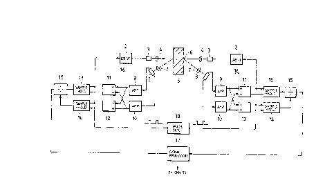
DETAILED DESCRIPTION OF THE PREFERRED EMBODIMENT
l An embodiment of the present invention will be
described with reference to Fig. 1, in which components
depicted by reference numerals 2 to 17 are the same as
those of the conventional device shown in Fig. 3 and, so,
details thereof are omitted. In Fig. 1, a pulse generator
18 is substituted for pulse generators 1 -used in the
conventional device shown in Fig. 3 for generating pulses
having waveforms a and b (Fig. 2) to be supplied to drive
circuits 2 and sample-hold circuits 13 and 14, alternatively
An operation of this embodiment will be described
with reference to the thickness measurement.
In Fig. 1, the pulse generator 18 supplies, to a
pair of the drive circuits 2, pulses having ON period
alternatively. The drive circuits 2 respond thereto to drive
light sources 3 such that light from the light source 3
associated with one of the drive circuits 2 has the waveform
a and that from the other light source 3 has the ~aveform b
The sample-hold circuits 13 and 14 sample the
signals according to the respective drive pulses and convert
them into d.c. components. That is, the sample-hold circuits
13 and 14 of one~of the deviation measuring means 16 perform
~ 2S
:' :
~: :
...... ,. . . . - ' '
~;~9~
-- 8 --
the sample-hold operation at a time instance t1 and the
sample-hold circuits 13 and 14 of the other deviation
measuring means 16 perform the sample-hold operation at a
time instance t2. The d.c. signals obtained in this manner
contain only light components o irradiating light of its
own system. Therefore, it is not influenced by irradiating
light in the other system even if the workpiece has a
transparency to light~
In a case of the step height measurement in which
both of the deviation measuring means 16 are disposed in one
side of the workpiece 5, light beams from the deviation
measuring means 16 are made alternative and, as in the
thickness measurement, one of the deviation measuring means
16 which~s emitting a light beam obtains a deviation by using
signals received thereby within a time for which it emits
the light beam. Therefore, it is not influenced by reflect-
ion light of light beam emitted by the other deviation
measuring means 16.
As mentioned above, according to the present
invention, it is possible to improve the accuracy of
thickness since the measuring in one deviation measuring
means is not influence~by light beam emitted by the other
, ~ :
even lf light beams are directed to a transparent workpiece
from opposite sides thereof.
~ Further, it is possible to improve the accuracy of
, : .
`
" ., .
~ ~295ilS29
step height measurement since the measuring in one deviation
measuring means is not influenced by light beam emitted by
the other even if both of the deviation measuring means are
; disposed in the same side of the workpiece.
::
: : :
: ~
: : :
~, ,
,~ :
: :
: