Note : Les descriptions sont présentées dans la langue officielle dans laquelle elles ont été soumises.
SUPERCONDUCTOR FOR MAGNETIC FIELD SHIELDING
Backqround of the Invention
1. Field of the Invention
The present invention relates to a superconductor for
magnetic field shielding which shields magnetic field~ using
superconductors.
2. Prior_Art
As a magnetic field shielding usiny superconductivity, firs't
or second class superconductors have been used depending on
the intensity of the magnetic field. A superconductor for
magnetic field shielding comprising a fixst class
superconductor uses perect diamagnetism (Meissner effect), a
property of superconductivity. The superconductor cannot
shield intense magnetic fields since its critical magnetic
flux density is low. A superconductor for magnetic field
shielding comprising the second class superconductor utilizes
both the superconductive and normal states, and its critical
magnetic field is separated into the upper and lower critical
magnetic fields. Since the intensity of the upper critical
:magnetlc field is extremely high, a superconductor comprising
~k
~ ~ 8~
the second class superconductor can belused to shield
intense magne-tic fields.
For magnetic field shielding using the second class
superconductor, what is called "electromagnetic
shielding" using the interlinkage magnetic flux
unchangeability principle can also be used to shield
intense magnetic fields.
When the above-mentioned superconductor is used to
shield magnetic fields, thin films of superconductor
layers are laminated. This kind of sh1elding can
perform stable shielding for a relatively in-tense
magnetic field in the thin region of the superconductor
layers. If the intensity of the magnetic field is very
high, that is, close to the intensity of the upper
critical magnetic field of a superconductor, heat is
generated by magnetic flux flow, and the shielding
effect is completely lost (secondary harmful
effec-ts). If a shielding comprises a plurality of
thick superconductor film layers (10 layers of
approximately 20~um thick films for example), the
above-mentioned harmful effects may be caused even when
the lntensity of the magnetic field is relatively low.
Accordingly, stability increases as the superconductor
\ , ' '
.. ......
layer is thinner.
The applicant of the present invention has previously
proposed a magnetic field shielding, which is a composite
lamination comprising thin superconductor film,layers and
metal and having a high magnetic field shielding effectO
This prior invention is characterized in that the
superconductor layers are made thinner than those made by the
conventional technology.
~owever, if such a superconductor is exposed in a magnetic
field, the magnetic field enters the superconductor layers
(there is a limit in this depth of entry, which is generally
referred to as entry depth of magnetic flux and is
approximately 500 A.) If the thickness of the superconductor
layer is smaller than this entry depth of magnetic flux,
almost all the magnetic fluxes pass through the layer and
shielding is impossible. If the intensity of the magnetic
filled exceeds that of the upper critical magnetic field, the
property of superconduction is usually lost and normal
conduction occurs.
In the case of the above-mentioned electromagnetic
shielding, such a superconductor must be joined using
solder, for example, to form a continuous conductor (a
closed circuit where electric current can flow).
Therefore, even when the conductor is made of
superconductor material with no resistance, the joint
section has a small resistance and thus the circuit has
a certain resistance. This electromagnetic shielding
can completely shield an intermittent magnetic filed,
but it cannot fully shield a uniform magnetic field
(magnetic field with a uniform intensity) since the
shielding effect drops as time passes due to the above-
mentioned resistance. This kind of electromaynetic
shielding is used only to shield fluctuating magnetic
field and thus has a very narrow application range.
When electromagnetic shielding is used to shield a
large area of field, a plurality of superconductor
coils are used. In this case, the magnetic field leaks
from the clearances between the superconductor coils
and thus no high shielding effect is obtained. A
net-like shielding can be devised by eliminating the
clearances between the superconductor coils. However,
producing this kind of shielding requires much lahor to
join superconductors in network. Furthermore, if it is
:
'~ .
. . ~. ~. .
necessary to shield a magnetic field with higher intensity, the
network shielding needs to be laminated into multlple layers.
The volume becomes relatively larger and the shielding suppor-t
layer must also be made larger. This requires much more amount
of refrigerant.
Summary of the Invention
It is -therefore an ob~ect of -the present invention to
provide a superconductor for magnetic field shielding mainly
comprising the second class superconductor.
After examining the above-mentioned problems, the
inven-tors of the present invention succeeded in development of a
superconductor for magnetic field shielding with an extremely
high shielding effect by ~ully utilizing the features of the
above-mentioned superconductive shielding and electromagnetic
shielding.
According to the present invention there is provided a
superconductor for magnetic field sh~elding comprising a
substrate, at least one superconductor film layer, which is
laminated on said substrate, and a plurality of small holes which
pass through said substrate and said superconduc-tor film layer,
wherein the thickness of said superconductor film layer is 100
or lessO
The present invention is detailed referring to the
following drawingsO
The invention will now he described in more detail, by
way of example only, with reference to the accompanying drawings,
in which:
`
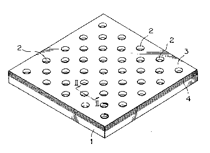
Fig. 1 is a perspec-tive view illustrating an example of
-the superconductor for magnetic field shielding of the present
invention, and
Fig. 2 is an enlarged vertical
- 5a -
sectional view taken on line II-II of ~ig. 1.
Detailed Description of the Invention
The present invention provides two basic embodiments.
One embodiment has a single superconductor film layer
and the other embodiment has a plurality of
superconductor film layers. These are selected
according to the intensity of the magnetism to be
shielded. Referring to Figs~ 1 and 2, the former
embodiment is a superconductor for magnetic field
shielding comprising a substrate 1, at least one
superconductor film layer 3, which is laminated on the
substrate 1, and a plurality of small holes 2 which
pass through the substrate 1 and the superconductor
film layer 3. The thickness of the superconduc-tor film
layer 3 is 100 ,um or less.
The lamina-tion shown in Figs. 1 and 2 is detailed below
in the description of Examples 4 to 7.
Metal, such as copper, aluminum, nickel or stainless
steel, or organic high molecular material, such as
polyester, polyphénylene sulfide, vinylidene chloride,
polyimide or polyether sulfone is used for the
substrate 1. The substrate has a plurality of small
holes 2. The area of one small hole 2 should be 3 cm~
,
'
'
6~
or less. The ~real por~sity in the e~tire area of the
substrate 1 should be 90% or less.
The small hole 2 can have a shape of circle, square or
many other shapes. Superconductor material, such as
niobium, niobium compound, niobium alloy, vanadium
compound or vanadium alloy is used for the above-
mentioned superconductor film layer 3. More
specifically, Nb, Nb-Ti alloy, Nb-Zr alloy, NbN, NbC,
Nb3Sn, Nb3Al, Nb2Ga, Nb3Ge, Nb3AlGe or V3Ga is used.
In addition, ceramic-based perovs]cite superconductor
material (for example Ba-Y-Cu-O compound and La-Sr-Cu-O
compound) and Chevrel superconductor material (for
example PbMo6Sg) are also used. These come under the
category of the second class superconductor and has the
:::
; above-menttoned characteris-tics. The kind of material
should be determined depending on the intensity of the
:: :
~ ~ magnetic field to be shielded. In actual practice,
: ~
however, Nb-Ti alloy is the best suited.
The latter comprises~the substrate 1, a plurality of
;; supérconductor film layers 3 and metal layers 4 (these
layers are lamlnated alternately on the substrate 1)
:
and a plurality of small holes 2 passing -through the
lamination. The thickness of the superconductor film
:: : ~ ,
.
. .
-- .
.
&~
layer 3 is 100 ~lm or less and the top layer of the
laminated material is the superconduc-tor film layer 3.
~ligh-purity aluminum and copper are ideally suited for
the metal film layer 4 sandwiched between the
superconductor film layers. Silver is also suited.
These metals of low purity or other metals can also be
used. The superconductor film layers 3 and the metal
film layers 4 are usually made by sputtering or
electron beam evaporation sequentially. The area of
the small hole 2 should be 3 cm~ (preferably 1 ~m~ to
0.75 cm2). The open area ra-te of the substrate 1 to the
small holes should be 90~ or less. If the area or rate
is larger, -the lamination has less strength and is
adversely affected when it is subjected to stress
caused by an intense magnetic field or when it is
handled. If the area is too small, clogging is apt to
occur during evaporation, and the area of the
superconductor film layers 3 becomes small. ~s a
result, the shielding current required to shield an
intense ma~netic field Icurrent flows to generate the
magnetic field which cancels the environmental magnetic
field) becomes small. If the open area of the small
hole 2 e~ceeds 3 cml, an inclination occurs at the
."^ . .~ . ~ ,...
.,~ .. ~............................................. .
shielding magnetic field in each smal~ hole 2.
Complete shielding cannot be conducted at each hole.
If the superconductor film layers 3 exceeds 100~um,
stable shielding canno-t be obtained when excitation is
quick. ~n this respect, the effect is more stable as
the superconductor film layers 3 is thinner.
In the above-mentioned superconductor for magnetic field
shielding, electromagnetic shielding is performed at
the small hole sections and superconductive shielding is
performed at the other sections using complete
diamagnetism and mixed-condition diamagnetism. These
two shielding effects are taken synergistically and
extremely high magnetism shielding can be performed.
In the case of electromagnetic shielding, shielding
current flows in the closed circuit composed of a
superconductor to cancel the magnetic field to be
shielded by generating the magnetic field whose force
direction is opposite to that of the magnetic field to
; be shielded. As the critical current density of the
superconductor increases, intense magnetic field can be
; shlelded more efficiently and stably.
By making the superconductor film layer 3 thinner, the
intensity of the upper critical magnetic field and
-: ,
~ 9
" ~ ~
:
-
,
,
critical current density of the layer,become largerthan those of the bulk of the similar kind. Therefore,
the shielding of the present invention ~evised by
combining the above-mentioned two shielding methods can
be used to shield extremely intense magnetic fields.
Accordingly, a relatively smaller amount o~
superconductor material is required to shield the
magnetic ~ield of the desired intensi~y.
~nlike the above-mentioned network shielding, the
magnetic shielding of the present inven-tion has no
joining section, or soldering section to form closed
circuits. When the magnetic shielding is used at a
temperature below the critical temperature, -the entire
resistance of the closed circuit (circumference of the
small hole) to be shielded becomes zero. Comple-te
shielding is thus possible regardless of whether the
magnetic field to be shielded is uniform or variable.
The superconductor for magnetic field shielding of the
present invention has limitless applications.
Furthermore, unlike a magnetic shielding sheet which
has not any small holes such as small holes 2 in the
substrate 1 of the present invention, re~rigerant can
enter the interiors of the small holes and the entire
\
area can be fully cooled. In a magnet,ic field of a
high intensity, magnetic fluxes can be forcibly trapped
at the small hole seetions to prevent heat generation
due to magnetic flux flow. Therefore, extremely stable
effect is obtained even in a magnetie field of a high
intensity.
As described above, as the superconductor film layer 3
becornes thinner, the effect is stabler. Even if the
thickness of the superconductor film layer 3 of the
present invention is made smaller than the entry depth
of magnetic flux, the superconduc-tor for magnetic field
shielding of the present invention can shield a
magnetic field whose intensity is higher than that of
the upper critical magnetie field of the bulk of the
similar kind due to the following reasons. Since the
entry depth of magnetie flux is larger than the
coherence length ~depth from the superconductor surface
where superconductor electrons can exist) in the case
of~the seeond elass supereonductor, the electrie
: : ~ ~: :
resistanee remains zero even when the thiekness of the
film layer is~smaller than the entry depth of the
magnetie field. The intensity of the upper critieal
magnetie field for the shielding of the present
~ .
.
invention is considerably higher than that for the bulk
of the similar kind.
When the thickness of the above-mentioned conventional
superconductor for magnetic field shielding made of
thin film lamination is made smaller tllan the entry
depth of magnetic flux to obtain a stable effect, the
most part of the magnetic field passes through the
superconductor regardless of the in~tensity of the
magnetic field and the number of superconductor layers,
and shielding is impossible. The superconductor for
magnetic field shielding of the present invention
performs electromagnetic shielding.i Even when the
thickness of the superconductor film layer is smaller
than the entry depth of magnetic flux, shielding
current flows due to zero resistance of the
superconductor layers and the magnetic shielding effect
is thus not lost.
When a plurality of superconductor film layers are used
for the superconductor for magnetic field shielding of
the~present invention, the metal film layer 4, made of
Cu, ~1 or Ag, is sandwiched between the superconductor
:: :
film layers~3. The metal film layer 4 is useful to
stabilize (mainly cool) the superconductor film layers
: ~ '
~ ~ 12
: '.: ~ ~
3. More particularly, the heat conductivitY of the
superconductor film layers 3 is very high and the all
superconductor film layers 3 can have higher heat
radiation effect. Temperature rise due to magnetic
flux flow is prevented. Current branches are formed at
portions where the superconduction state is converted
into the normal conduction sta-te to prevent heat
generation and to restore the superconduction state.
When a plurality of superconductor layers are exposed
to an intense magnetic field, the first layer is
affected most seriously by the magnetic field. The
second and the subsequent layers are less affected.
The intensity of the magnetic field becomes nearly zero
at the final layer. This shielding function is
possible only when all layers operate stably. If a
flux jumping occurs at the first layer for e~ample, an
abrupt magnetic field change occurs at the second
layer, and a flux jumping also occurs at the second
layer, resulting in that the desired magnetic field
shielding effect cannot be obtained.
Since the superconductor for magnetic field shielding
of the present invention is a composite lamination of
metal layers 4 having the above-mentioned function
.
.
~ ~ 13
~ ~ .
,, ., ,, ~ . - ~ -
~2~
sandwiched between the superconductor film layers 3 and
the small holes 2 are disposed to forcibly prevent
magnetic flux flow, the above-mentioned flux jumping is
prevented and the superconductor layers 3 are stabilized.
Thus, the characteristics of the superconductor layers
can be fully utili~ed.
Embodiment examples and comparison examples are
described below.
(a) Three polyphenylene sulfide sheets having a thickness
of 50Jum were prepared. These were used as
substrates 1. Small square holes 2 (with a side 3 mm
long) were disposed in each substrate 1 so that the
areal porosity of the substrate were 30%, 80%
and 91~, respectively.
A 10 ~m thick film of Nb-Ti alloy was produced on one
side of each substrate 1 by sputtering method without
applying heat to form a superconductor film layer 3
made of Ni-Ti alloy. In this way, three types of
composite laminations were formed and classified as
embodiment example 1, embodiment example 2 and
comparison example 1 ( areal porosity of 30~, 80%
and 91~ respectively).
; Each of the above-mentloned composite laminations was
~ 14
.() Al:'`.'J
processed to take a shape of a disc of 45 mm in
diameter. The amount of magnetic field shielding was
measured at the center of each disc. The amounts
were 0.052, 0.012 and 0.000 Teslas for embodiment
example 1, embodiment example 2 and comparison
example 1 respectively. Accordingly, if the areal
porosity exceeds 90~, the shielding effect is almost
lost, and such a shielding lamination has less
strength and is adversely afEected when it is
subjected to stress caused by a magnetic field or
when it is handled.
Two 30,um thick Ni sheets were prepared. These were
used as substrates 1. Small holes 2 of 30~um in
diameter were disposed in the substrates so that the
areal porosity of each substrate was approx. 5%.
In the same way as the above item (a), a 10 ~lm thick
film of Nb-Ti alloy was produced on one side of each
substrate 1 to form a superconductor film layer 3
made of Ni-Ti alloy. In this way/ two types of
composite laminations were obtained and classified as
embodiment example 3 and comparison example 2 (with
no small holes).
The magnetic field shielding amount for embodiment
::
1 5
, . . .
$9
example 3 was 0.089 Teslas and that ~or comparison
example was 0.072 Teslas. It is understood that the
composite lamination with no small holes has less
magnetlc field shielding effect.
Five 30 ym Ni sheets were pxepared and these were
used as substrates i. Small holes 2 of approx. 50~um
in diameter were disposed in the substrates 1 so that
the areal porosity of the substrates was approx. 5%.
Using the same sputtering method as described above,
10 superconductor fllm layers 3 (made of Nb-Ti alloy)
and 10 metal ilm layers 4 (made o 99.99~ Cu) were
formed alternately one by one to obtain the following
five kinds of composite laminations~ In this case,
the thickness of the metal film layer 4 is a constant
value of 2 ~m. The thicknesses of the superconductor
film layers 3 of the five types of composite
laminations were 1 ~m, 10 um, 30Jum and 100~um
respectively. These were classiied as embodiment
examples 4, 5, 6 and 7, and comparison example 3.
Figs. 1 and 2 show an example o these composite
laminations.
In the figures, the metal ilm layer 4 just above the
substrate 1 can be omitted. Each metal film layer 4
:
: : :
: ~ ~ 16
.
'
should only be sandwiched between the superconductor
film layers 3. The number of the lamination layers
shown in Fig. 1 differs from that oE the layers shown
in Fig. 2 since some layers are not shown in Fig. 1
for convenience.
The magnetic field shielding amounts for these
composite laminations were measured in the same way
as described above. The amount for embodiment
example 4 was 0.20 Teslas, -that for embodiment
example 5 was 0.88 Teslas, that for embodiment
example 6 was 0.98 Teslas, that for embodiment
example 7 was 1.1 Teslas and that for comparison
example 3 was 0.75 Teslas.
According to these results, in the superconductor for
magnatic field shielding laminated as described
above, the stabiliza-tion effect increases and the
shielding effect corresponding to the amount of
superconductor material also increases as the
superconductor ~ilm layer 3 is thinner. In the case
of the lamination of 150 ~Im superconductor film
layers such as those usad or comparison example 3,
:
the magnetic field shielding amount is relatively
high, but tha shieiding effect becomes unstable
17
., ,,, ., ., . ~ .
:
~;~G.J ~¢ ~9
sometimes. If excitation is quick, ~agnetic flux
jumping may occur, bringing poor shielding effect.
This causes problems when such a lamination is put in
practical use.
(d) A 50 ~um thick copper sheet was used as the substrate
1. Small holes 2 of 3 mm in diameter were disposed
so that the areal porosity of the substrate 1 was 40~.
One hundred superconductor film layers 3 made of NbC
compound (the bulk's upper critical magnetic field of
1.69 Teslas) and 100 metal film layers 4 made of
99.99~ aluminum were laminated alternately one by one
the substrate 1 by responsive sputtering method while
the substrate 1 was heated in the atmosphere of
methane-argon mixture gas. The composite lamination
obtained in this way was classified as emhodiment
example 8. The thickness of the superconductor film
layer 3 of this embodiment example was 400 ~ and the
thickness of the metal film layer 4 was 1000 A.
Forty composite laminations of embodiment example 8
was exposed to the magnetic field intensity of 1.8
Teslas. The measured magnetic field shielding amount
was approx. 0.3 Teslas.
As a result, it is understood that even the magnetic
:
18
.
field stronger -than the bulk's upper critical
magnetic field can be shielded using the above-
mentioned extremely thin superconductor film layers
3. This is explained as follows. When the
superconductor film layer 3 is thinner than the entry
depth of a magnetic flux, the intensity of the upper
critical magnetic field increases and a close~
circuit is formed around each small hole 2. The
normal superconductive shielding and elec-tromagnetic
shielding are thus performed simultaneously. By
laminating a plurality of layers, more complete
shielding is possible. The stabilization effect is
superior since the superconductor film layers 3 are
very thin.
Instead of Nb-Ti alloy or NbC compound used as the
above-mentioned superconductor film layers, other
superconductor materials can function as described
above although there are differences in the actual
mea~surement values. This has been confirmed by the
experiments conducted by the inven-tors of the present
:
inven-tion~ E~owever, the function of the
; superconductor material of embodiment example 8 with
an extremely intense upper critical magnetic field is
19
:: : :
~l
not yet confirmed since the magnetic field to be used
for confirmation cannot be generated by the currently
available technology. Nevertheless, it is easily
known by analogy that superconductors other than NbC
can function as described above. It is expected that
the magnetic field shielding effect will increase in
the magnetic field having the intensity higher than
that of the upper critical magnetic field by
sandwiching a dielectric film layer (instead of or
together with the metal film layer) between the
superconductor layers.
As described above, in the superconductor for
magnetic field shielding of the present invention,
shielding by diamagnetism of superconductor and
electromagnetic shielding due to the closed circuits
formed at the small hole sections are performed
simultaneously, resulting in delivering an extremely
high shielding effect regardless of whether the
magnetic fleld is uniform or variable. In addition,
the above-mentioned magnetic field shielding
characteristics, the small hole sections and the metal
film layers between the superconductor film layers
function synergistically so that the superconductor
:
~ 20
,i,, ..,,"..~,.
~:
can be extremely stable even in an intense magnetic
field. Therefore, the superconductor of the present
invention is regarded as a completely innovative
superconductor for magnetic field shielding. If this
invention is applied to various magnetic field
shielding devices, it is obvious that the
superconductor of the present invention is useful for
reduction of the weight and cost of such devices, and
stabilization of the devices. Fur-thermore, the
superconductor of the present invention can be formed
more easily since it is made of thin films. It is
certain that the superconductor of the present
invention will be highly evaluated in many fields as
a superconductor for magnetic field shielding of very
high practical use~
:
:
~: :
21
Il~' ~I" '' I" "
. . :