Note : Les descriptions sont présentées dans la langue officielle dans laquelle elles ont été soumises.
3~
The present invention relates generally to a
method for controlling a frequency converter, and to a
frequency converter designed to apply the method. The
frequency circuit described herein has multiple output
times at different phases of the same frequency.
In a frequency converter, a constant-frequency
a.c. mains voltage is connected to a rectifying unit. The
power is taken from the mains, and the rectiEied (d.c.)
voltage is converted by an inverting unit into a variable~
frequency (a.c.) voltage to feed the load. In frequency
converters, either the current or the voltage is
controlled. The desired amplitude and frequency values are
set for the current or the voltage, while the value of the
other parameters, which are not controlled, is determined
by the supply and the loading conditions.
In voltage-controlled frequency converters the
desired voltage for feeding the load is producea for
example via pulse-width modulation, whereby sinusoidal and
triangular waves are compared to produce the control pulses
for driving the semiconductor switches in the power stage
of the frequency converter. A disadvantage of vsltage-
` controlled frequency converters is the noise produced in
the motors constituting the load, such noise being the
result of the wave form of the voltage fed into the load.
If current is the controlled parameter in the
frequency converter, the control signals for the
semiconductor switches can not be produced in the manner
referred to above. The reason is that in current-
controlled frequency converters, current can flow only in
one direction at both ends of the bridge circuits.
Moreover, a path must be provided for the current of the
intermediate d.c. circuit permanently, and when the
parallel-connected transistors of the bridge are driven
simultaneously, current can only flow through the one of
the transistors which has the higher collector-emitter
voltage. In current-controlled frequency converters it is
.
~6;3~3~
difficult to obtain a suitable waveform for the mains and
load currents. A further disadvantage is the generation of
harmonics.
Methods for controlling a ~requency converter in
which the currents of the frequency converter are
controlled via modulation in such a manner that the current
modulation periods of each phase are interlaced with the
modulation periods of the other phases are known. By such
methods, a suitable waveform is obtained for both mains and
load currents and the generation of harmonics is reduced to
a minimum.
It is also known in the art to provide a path for
the current when the momentary value of each phase current
taken from the mains and supplied to the load is zero, by
turning on the semiconductor switches of one of the phases
when normally none of the switches is conducting.
The modulation circuits of known current
controlled inverters, as the modulation circuits in the
inverters of U.S. Patent Nos. 4,578,746 and 4,581,69~, are
made by using counters and dividers. Various waveforms can
be obtained using counters and dividers. The disadvantage
is that a failure whan counting or dividing may cause a
harmful disturbance in the transistor bridge.
An object of the present invention is to minimize
ti,~ drawbacks of modulation circuits of multi-phase current
controlled frequency converters having pulse controlled
semiconductor switches, by using a simple modulation method
which makes it possible to use simple components as
comparators and logic gates in said modulation circuit.
The invention will now be described in further
'~ detail with reference to the accompanying drawings in
which:
Figure 1 illustrates a current-controlled
frequency converter to which the modulator and modulation
method of the present invention may be applied;
-" ~291~ii3~3~
Figure 2a illustrates sinusoidal current reference
signals and a positive triangular carrier wave;
Figure 2b shows the preliminary control pulses for
the R-phase;
Figure 2c shows the preliminary control pulses for
the S-phase;
Figure 2d shows the preliminary control pulses for
the T-phase;
Figure 2e shows an auxiliary control signal for
zero diode function of the R-phase;
Figure 3a shows the positive modulation signal MR+
for the R-phase;
Figure 3b shows the negative modulation signal MR-
for the R-phase;
Figure 3c shows the positive modulation signal MS+
for the S-phase;
Figure 3d shows the negative modulation signal MS-
for the S-phase;
Figure 3e shows the positive modulation signal MT~
for the T-phase;
Figure 3f shows the negative modulation signal MT-
for the T-phase;
Figure 4a shows the combined modulation signal MR
for the R-phase;
Figure 4b shows the combined modulation signal MS
for the S-phase;
Figure 4c shows the combined modulation signal MT
for the T-phase;
Figure 5 illustrates the block diagram of the
modulation circuit; and
Figure 6 shows the modulation circuit.
In a preferred embodiment of the method of the
invention, in the first phase R the preliminary control
pulses iR+ for the semiconductor switch conducting during
the positive half-cycle of the phase and the preliminary
control pulses iR- for the semiconductor switch conducting
3'~3~3~
during the negative half-cycle are produced separately from
a combined modulation signal MR. This is accomplished by
comparing the positive half-cycle of the signal MR for the
semiconductor switch conducting during the positive half-
cycle to a positive triangular waveform signal I-~ and the
negative half-cycle of the signal MR for the semiconductor
switch conducting during the negative half-cycle to a
negative triangular waveform signal. The control pulses iS+
and iS- for the semiconductor switches of the second phase
S, are produced by comparing the positive part of a
combined modulation signal Ms for the second phase to a
positive triangular signal and the negative part of the
combined modulation signal Ms to a negative triangular
signal and further removing from the obtained pulses the
periods during which the control pulses iR are applied to
the corresponding first-phase semiconductor switches. The
preliminary control pulses iT+ and iT- for the third-phase
T semiconductor switches are produced by comparing the
positive parts of a combined modulation signal MT for the
third phase to a positive triangular signal, and the
negative part of the combined modulation signal MT to a
~` negative triangular signal and further removing from the
thus obtained pulses the periods during which the control
pulses are applied to the corresponding semiconductor
switches of the first and second phases.
The combined modulation signals are generated by
current reference signals as follows: MR corresponds to
current reference signal IRC; the positive part of Ms is
obtained by summing the positive parts of the current
reference signals for phases R and S and the negative part,
by summing the negative reference signals for phases R and
S; the positive part of MT is obtained by summing the
positive parts of current reference signals fcr phases R,
S and T, and the negative part of MT is obkained by summing
the negative parts of current reference signals for phases
R, S and T.
,. ~
38~
An alternative preferred embodiment of the method
of the invention is characterized in that the modulation i5
implemented using combined modulation reference signals
produced by removing from the curves of the second phase
(Ms+ and Ms~) the parts which coincide with the modulation
reference signals of the first phase (MR-~ and MR-) and from
the third-phase curves (MT+ and MT-) the parts which
coincide with the curves of the first and second phases.
The frequency converter used for applying the
method of the invention comprises a mains bridge which is
provided with controllable semiconductor switches, a motor
bridge likewise provided with controllable semiconductor
switches, and a control unit for controlling the
semiconductor switches, enabling the currents in the
frequency converter to be controlled via modulation in such
manner that the modulation periods for each phase can be
interlaced with the modulation periods of the other phases.
In a preferred embodiment of the frequency
converter for applying the method of the invention, the
control unit comprises at least one memory circuit where
the modulation control signals can be stored.
The control unit of the frequency converter of the
invention is provided with a zero diode circuit enabling
the provision of a path for the current when the momentary
value of the current taken from the mains and supplied into
the load in each phase is zero by turning on the
semiconductor switches of one of the phases when none of
these switches normally conducts, with a signal generated
for this end.
The preferred embodiment of the modulation circuit
,~. of the frequency converter applying the method of the
invention is characterized in that the control unit
contains NOR-gates or similar circuits, the first one of
which eliminates those parts of the preformed control
pulses for the transistor conducting during the positive
half-cycla of the second phase S which coincide with the
.
`` ~2~3~
preliminary control pulses for the transistor conducting
during the positive half-cycle of the first phase R.
second NOR gate eliminates those parts of the preformed
control pulses for the transistor conducting during the
negative half-cycle of the second phase S which coincide
with the preliminary control pulses for the transistor
conducting during the negative half-cycle of the first
phase R. A third NOR gate eliminates those parts of the
preformed control pulses for the transistor conducting
during the positive half-cycle of the third phase T which
coincide with the preliminary control pulses for the
transistors conducting during the positive half-cycles of
the first R and second T phases, while a ~ourth NOR gate
eliminates those parts of the preformed control pulses for
the transistor conducting during the negative hal~-cycle of
the third phase T which coincide with the preliminary
control pulses for the transistors conducting during the
negative half-cycles of the first R and second S phases.
According to the present invention, a method for
controlling a frequency converter wherein the currents of
the frequency converter are controlled via modulation in
such a manner that the current modulation periods of each
phase are interlaced with the modulation periods of the
other phases is disclosed.
According to a further aspect of the invention a
frequency converter comprising a mains bridge and a motor
bridge both having controllable semiconductor switches, and
a control unit for controlling said semiconductor switches,
whereby currents in the frequency conVerter are
controllable via modulation in such manner that the
modulation periods (i.e. the duration of control pulses) of
each phase can be interlaced with the modulation periods o~
the other phases.
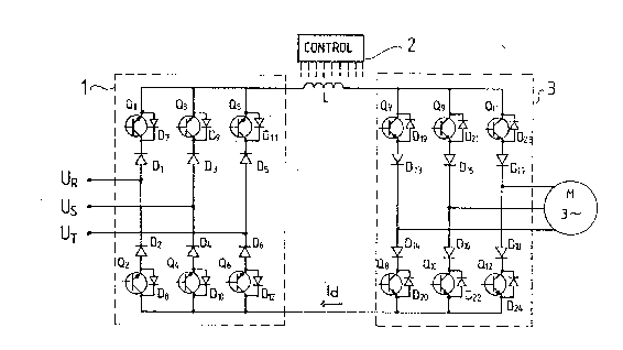
Figure 1 shows a current-controlled frequency
converter and a motor constituting the load. The frequency
converter contains a rectifier bridge 1 which rectifies the
3~3~
constant-frequency mains supply phase voltages u~, Us and
UT t produce the d.c. current Id for the d.c. circuit.
The mains rectifier bridge consists of diodes D1 - D6 and
transistors Q1 ~ Q6~ which are connected in series with the
said diodes and inverse-parallel connected zero diodes D7 -
D12. The transistors Q1 ~ Q6 are controlled by the controlunit 2.
The direct current Id, which is filtered by the
inductance L, flows in the d.c. circuit which feeds the
motor bridge 30 ~he motor bridge consists of diodes D13 ~
D18 and transistors Q7 ~ Q12 ~ which are connected in series
with the diodes, and inverse-parallel connected z~ro diodes
D18 ~ D24. Transistors Q7 - Q12 are also controlled by the
control unit 2. In the motor bridge 3 a three-phase
current is produced to feed the squirrel-cage motor M.
The control unit 2 produces the transistor control
signals separately for each of the two bridges. The
control unit 2 modulates both the current taken by the
frequency converter from the mains and the current supplied
to the load. This modulation is so implemented that the
modulation periods of each phase are interlaced with the
modulation periods of the other two phases. During each
modulation period, the average value of the phase current
corresponds to the desired waveform of the current, e.g. a
sine wave. A path is provided for the current even when
the momentary values of the currents taken from the mains
and supplied to the load M are zero.
When the control current waveforms desired are the
sinusoidal current reference signals IRC ~ ISC and ITC, as
shown in Figure 2a, the modulating action of the circuit is
as follows. (Figure 2a also shows positive and negative
summed waves IRSC~ ISTC~ and ITRC of current re~erence
signals). From the R-phase current reference signal IRC~
separate pulses iR-~ and iR- for the transistors Q1 and Q7
conducting during the positive half-cycle of the branch and
for the transistors Q2 and Q8 conducting during the negative
ji3~
half-cycle are produced. The positive half-cycle of the
current reference signal IRC for the transistor conducting
during the positive half-cycle is compared to a positiv~
triangular wave~orm signal I~, shown in Figure 2a, and the
negative half-cycle of the current control system IRC for
the transistor conducting during the negative half-cycle is
compared to a negative triangular waveform signal, which
is obtained from the positiva triangular waveform signal by
means of an inverting amplifier. This results in the
preliminary control pulses iR+ and iR- shown in Figure 2b in
which the positive pulses control the transistors
conducting during the positive half-cycle and the negative
pulses control the transistors conducting during the
negative half-cycle. The wave in Figure 2b consists of
positive and negative pulses (whose duration represents the
modulation periods), and intervals between pulses. The
modulation periods for the other two phases are pro~uced in
a corresponding manner, as described belo~7.
The preliminary control pulses for the transistors
Q3, Q4, Q9 and Q10 in the S-phase are produced as follows.
The positive current reference signals IRC+ and IsC+ for
phases R and S are added together and the sum obtained IRSC+
is compared to the positive triangular signal. Similarly,
the negative current control signals IRC- and ISc- for phases
R and S are added together and the sum IRSC- obtained is
compared to the negative triangular signal. ~he resulting
preformed control pulses correspond to the sum of the
control pulses for the transistors in phases R and S for
the modulation period in question. Removing from these
signals the portions during which the R-phase transistors
are being driven results in the preliminary control pulses
iS~ and iS for phase S as shown in Figure 2c, in which the
positive pulses control the transistors conducting during
the positive half~cycle and the negative pulses control the
transistors conducting during the negative half-cycle. As
can be seen from Figures 2a, 2b and 2c, when the positive
3~
half-cycles of the current control signals for phases R and
S occur simultaneously (doted IRSC+ signal on Figure 2a),
the preliminary control pulses iS+ for the S-phase
transistors conducting during the positive half-cycle occur
in the intervals between the preliminary control pulses iR+
for the R-phase transistors conducting during the positive
half-cycle. Similarly, the preliminary control pulses iS-
for the S-phase transistors conducting during the negative
half-c~cle occur in the intervals between the preliminary
control pulses iR- for the ~-phase transistors conducting
during the negative half-cycle. In this arrangement, the
duration of the total modulation period remains at the
desired value.
The control signals for the transistors Q5, Q6,
Q11 and Q12 in the T-phase are produced as follows. The
positive current reference signals IRC+ ~ ISC+ and ITC~ for
phases R and S and T are added together and the sum
obtained is compared to the positive triangular signal.
Similarly, the negative current control signals IRC- ~ ISC~
and ITC- for phases R and S and T are added together and
the sum obtained is compared to the negative triangular
signal. The resulting preformed control pulses correspond
to the sum of the preliminary control pulses for the
transistors in phases R, S and T for the modulation period
in question. Removing the portions of these preliminary
control pulses during which the transistors of the R and S
phases are being driven, results in the signals iT~ and iT
for phase T as shown in Figure 2d, in which the positive
pulses control the transistors conducting during the
positive half-cycle and the negative pulses control the
transistors conducting during the negative half-cycle~ The
preliminary control pulses for the T-phase transistors
conducting during the positive half-cycle now occur in the
intervals between the preliminary control pulses for the R
and S phase transistors conducting during the positive
half-cycle and the preliminary control pulses for the T-
~Z9Ç~3t~4
phase transistors conducting during the negative half-cycle
occur in the intervals between the preliminary control
pulses for the R and S phase transistors conducting during
- the negative half-cycle.
Moreover, both transistors of the rectifying and
inverting bridges of the R-phase are turned on in the
intervals in which none of the bridge transistors
conducting during the positive and negative half-cycles are
receiving their normal control pulses. This ensures that
a path through the bridge is provided for the current Id of
the d.c. circuit. To provide for this zero diode action of
the frequency converter, an additional pulse train io as
shown in Figure 2e for controlling the R-phase transistors
is produced.
When the modulation control signals for the
transistors are generated from the sinusoidal current
reference signals as described above, the resulting
waveforms are as shown in Figures 3a-3f, of which Figure 3a
shows the positive modulation signal MR+ for phase R, Figure
3b the negative modulation signal MR- for phase R, Figure 3c
the positive modulation signal Ms+ for phase S, Figure 3d
the negative modulation signal Ms~ for phase S, Figure 3e
the positive modulation signal MT+ for phase T, and Figure
3f the negative modulation signal MT- for phase T. Since
the transistors of the bridge conducting during the
positive half-cycle and the transistors of the bridge
conducting during the negative half-cycle are turned on in
a definite order R - S - T, if an attempt is made to make
them conduct simultaneously, it is possible to remove the
parts of the S-phase modulation signal Ms+ respectively Ms~
(shown in Figures 3c and 3d) which coincide with the
modulation signals MR+ respecti~ely MR- for phase R as well
as the parts of the T-phase modulation signal MT+ ~
respectively MT- shown in Figures 3e and 3f which coincide
wi~h the modula~ion signals for phases R and S. By
combining the modulation signals as described for the
3~
11
transistors conducting during the positive and negative
half-cyclas of each phase w~ obtain the combined modulation
signals MR~ M5 and MT shown in Figures 4a ~ 4c. If the
sinusoidal current reference sigllals IRCI ISC and ITC are
replaced with these combined modulation signals, MR, MS and
MT no half~wave rectifiers or adder circuits are needed in
the modulation circuits described below. The wav~form for
the modulation control signals for the transistors of the
mains and motor bridges are similar. The frequency of the
mains bridge modulation control signal is constant, whereas
the frequency of the modulation control signal for the
motor bridge varies.
Figure 5 shows the block diagram of the modulation
circuit. Figure 6 shows the modulation circuit itself. A
separate modulation circuit is provided in the control unit
2 for each of the two bridges.
The modulation is effected in the manner described
above, by comparing a positive and negative triangular wave
form signal of a freguency o~ e.g. 2 kHz, supplied by a
carrier generator 5, to the combined modulation control
signals MR/ MS and MT shown in Figures 4a - 4c. For phase
R, separate preliminary control pulses iR+ and iR_ are
produced for the transistor conducting during the positive
half-cycle and for the transistor conducting during the
negative half-cycle. The positive modulation signal MR+ for
the transistor conducting during the positive half-cycle is
compared to the positive triangular wave, and the negative
modulation signal MR- for the transistor conducting during
the negative half-cycle is compared to the negative
triangular wave in the modulator 4, into which the combined
modulation signal MR and the triangular waves are fed.
For the S-phase transistors conducting during the
positive half-cycle and those conducting during the
negative half-cycle, the preliminary control pulses iS+ and
iS- respectively are produced by the modulator 4 by
comparing the positive half-cycle of the modulation signal
12
Ms+ to the positive triangular signal and the neyative half-
cycle of the modulation signal Ms~ ~o the negative
triangular signal and after the comparison, feeding the
resulting signal into a differential circuit 6 to remove
those parts for which a coincidence with the control
signals for the R-phase transistors has been detected.
For the T-phase transistors conducting during the
positive half-cycle and those conducting during the
negative half-cycle, the preliminary control pulses iT+ and
iT- respectively are produced by the modulator 4 by
comparing the positive half-cycle of the modulation signal
MT+ to the positive triangular signal and the negative half-
cycle of the modulation control signal MT- to the negative
triangular signal. The obtained signals are then fed into
a differential circuit 7 to remove the parts of the
resulting signal for which a coincidence with the
preliminary control pulses for the transistors of the R and
S phases has been detected.
For the R-phase bridge transistors, the zero diode
function, which enables them to conduct when normally none
of the transistors conducts, is achieved by applying the
preliminary control pulses for the R-phase transistors to
a zero diode circuit 8 which adds to these signals the
required auxiliary controi signal io, shown in Figure 2e.
Finally, all the preliminary control signals are
passed to the transistor base current amplifiers through a
protective amplifier 9, which ensuxes that the transistors
can be turned off in case of mal~unction and control pulses
SR+ ~ ST_ for each phase are obtained.
Figure 6 shows the current modulation circuit.
The combined modulation signal MR for phase R, shown in
Figure 4a is obtained e.g. from an EPROM memory circuit
10a, the combined modulation signal Ms for phase S, from
another EPROM circuit 10b and the combined modulation
signal MT for phase T, from a third EPROM circuit 10c. The
combined modulation signals, the positive triangular
38~
13
waveform signal, obtained from the carrier wave generator
ll, and the negative triangular waveform signal, obtained
from the positive triangular signal after an inverting
amplifier 12, are fed into the modulator ~. The modulator
generates the preformed control pulses for the transistors
conducting during the positive half-cycle by comparing the
positive triangular wave to the combined modulation signals
in operational amplifiers 14a, 14c and 14e, and the
preformed control pulses for the transistors conducting
during the negative half-cycle by comparing the negati~e
triangular wave to the combined modulation signals in
operational amplifiers 14b, 14d and 14f. Next, the parts
of the preformed control pulses for the transistor
conducting during the positive half-cycle of the S-phase
which coincide with the preliminary control pulses for the
transistor conducting during the positive half-cycle of the
R-phase are removed by the NOR gate 15a acting as a
differential circuit, and the parts of the preformed
control pulses for the transistor conducting during the
negative half~cycle of the S-phase which coincide with the
preliminary control signal for the transistor conducting
. during the negative half-cycle of the R-phase are removed
by the NOR gate 15b acting as a differential circuit.
Similarly, the parts of the preformed control pulses for
the transistor conducting during the positive half-cycle of
the T-phase which coincide with the preliminary control
pulses for the transistors conducting during the positive
half-cycles of both R and S phases are removed by the NOR
gate 15c acting as a differential circuit, and the parts of
the preformed control pulses for the transistor conducting
during the negative half-cycle of the T-phase which
coincide with the preliminary control pulses for the
transistors conducting during the negative half-cycles of
the both R and S phases are removed by the NOR gate 15d
acting as a differential circuit.
~g~3t3~
14
The preliminary control pulses are fed into the
zero diode circuit 16, which provides an additional control
signal for the R-phase transistors when normally none o~
the transistors conduct. To achieve this, the positive
preliminary control pulses are first applied to NOR gate
17a and the negative preliminary control pulses to NOR gate
17b. The output of each of these gates is applied to a
third NOR gate 17c. The output of NOR gate 17c and the
preliminary control pulses for phases S and T are applied
to four NAND gates 18a-18d respectively. This ensures that
during the periods when the auxiliary control signal for
the R-phase transistors exists, no control signal is
applied to any of the transistors of the other phases, so
that none of them conduct. In the R-phase, the auxiliary
control signals are obtained by applying the output of the
above-mentioned NOR gate 17c via an inverting amplifier 19
to two further NOR gates 2Oa and 2Ob, the first of which
rsceives at its other input the preliminary control pulses
iR~ for the transistor conducting during the positive half-
cycle and the second, the preliminary control pulses iR- for
the transistor conducting during the negative half-cycle.
Next, all the preliminary control pulses thus processed are
fed into protective amplifiers 21a - 21f which invert the
signals and pass them on to the transistor base current
amplifiers (which are not shown in the Figures) as control
pulses SR+ ~ ST-~ In case of malfunction, the protective
amplifiers can disconnect the control signals to the
transistors.
It will be obvious to a person skilled in the art
that the invention is not restricted to the above examples
of its embodiments, but that it may instead be varied
within the scope of the following claims.