Note : Les descriptions sont présentées dans la langue officielle dans laquelle elles ont été soumises.
1~Z968~6
-- 1 --
1 TITLE OF THE INVENTION
Process for Producing a Semiconductor Article
BACKGROUND OF THE INVENTION
Field of the Invention
The present invention relates to a process for
producing a semiconductor article, specifically to a
process for producing a semiconductor article by applying
crystal formation treatment to a substrate having a
free surface on which a nonnucleation surface exhibiting
a smaller nucleation density and a nucleation surface
exhibiting a larger nucleation density and having a
sufficiently minute area so as to allow only a single
nucleus to be formed thereon are disposed next to each
other, whereby a monocrystal is permitted to grow from
the nucleus.
The present invention is applicable to the
formation of monocrystals, polycrystals, etc. for
electronic devices, optical devices, magnetic devices,
piezoelectric devices, surface acoustic devices, etc.
including semiconductor integrated circuit, optical
:
1ntegrated circuit, magnetic circuit, etc.
Related Background Art
In the prior art, monocrystalline thin film to
be used for semiconductor electronic devices, optical
devices, etc. has been foxmed by epitaxial growth on a
:: :
monocrystalline substrate. However, for epitaxial growth
~:
:~L296;8~;
- 2 -
1 of monocrystalline thin film on a monocrystalline
substrate, it is necessary to take matching in lattice
constant and coefficient of thermal expansion between
the monocrystalline materials of the substrate and the
epitaxial growth layer, and there has been involved
the problem that the kind of substrate material is
limited to an extremely narrow scope for formatlon of
monocrystalline layer capable of providing a device of
good quality.
Further, in recent years, research and development
have been actively done about three-dimensional integrated
circuits for accomplising high integration and multi-
functionality by forming semiconductor devices by
lamination in the direction normal to the substrate,
and also research and development about large area
semiconductor devices such as solar battery in which
elements are arranged in an array on an inexpensive
glass or switching transistor for liquid crystal picture
elements, etc. are becoming more active year by year.
What is common in these researches and developments
is that the technlque to form a semiconductor film on an
amorphous insulating material and form an electronic
device such as transistor, etc. thereon is required.
Among them, it has been particularly desired to have a
technique to form a monocrystalllne semiconductor film
of high quality on an amorphous insulating material.
However, generally speaking, when a thin Eilm
~2~
- 3 - ,
I is formed on an amorphous insulating substrate such as
SiO2, etc., due to deficiency of long length order of
the substrate material, the crystal structure of the
deposited film will become amorphous or polycrystalline,
whereby it is vexy difficult to form monocrystalline
semiconductor of high quality. Here, amorphous film
refers to one with the ~tate in which although short
length order to such an extent as the minimum order of
neighbor atoms may be maintained, there is no particular
order of longer length, while polycrystalline film-
refers to one in which monocrystal grains having no
specific crystal direction are gathered as separated
with grain boundaries.
As a solution of the problems as mentioned
above in the prior art, European Patent Application
EP 244081Al p oposes a method for forming crystal by
preparing a substrate having a nonnucleation surface
having a small nucleation density and a nulceation
surface having a sufficiently larger nucleation density
20 than t~e nonnucleation surface and a minute area such
that only a slngle nucleus can be formed, then forming
a single nucleus on the nucleatlon~surface and permitting
a monocrystal to grow from the single nucleus as the
growing center, and it is shown possible to form a
25 monocrystal even on the substrate surface of amorphous
materlal by use of the above method.
On the other hand, semiconductor clevices s~ch
as MOS type transistor, bipolar transistor, SCR, etc.
-
~Z~6B9~
- 4 --
I are constituted of a plural number of p-n junciton
portions formed in combination. For example, in the
case of a p-channel MOS type transistor, the device is
constitutied of p-type semiconductor regions as source
region and drain region formed in an n-type semiconductor
region.
To form such a semiconductor device on an
insulating amorphous substrate by use of the crystal
forming method described in the European Patent Application
10 EP 24~081Al, a facet of monocrystal is permitted to
grow on the substrate, and after flattening of the facet
oE monocrystal, the conventional semiconductor device
production process i5 practiced. More specifically,
after a certain conduction type semiconductor region
is formed, ion implantation of n-type impurity or p-type
impurity is practiced.
However, the above semiconductor device formation
requires ion implantation and diffusion steps thus being
complicated while it involves essential difficulty in
separate formation of semiconductor regions with high
precision which may be attributed to the difficulty in
controlling the diffusion process.
SUMMARY OF THE INVENTION
An object of the present invention is to provide
a process for producing a semiconductor article enabling
easily forming semiconductor regions having different
... . .
- s - ;
characteristics, e.g. conduction type as mentioned above,
in a monocrystal thus simplifying the production steps
si.gnificantly.
The inventive process for pxoducing a semiconductor
-
article comprises applying crystal formation treatment
to a substrate having a free surface on which a non-
nucleation surface exhibiting a smaller nucleation
density and a nucleation surface of an amorphous
material exhibiting a larger nucleation density and
having a sufficiently minute area so as to allow only
a single nucleus to be formed thereon are disposed next
to each other whereby a semiconductor monocrystal is
permitted to grow from the nucleus, the production
conditions during said crystal formation treatment being
varied to form semiconductor crystal regions different
in their characteristics within at least part of said
semiconductor monocrystal.
Here, the term 'monocrystal' means one having
a substantially monocrystalline structure regardless
Of existance of some lattice defects.
:
~ In the present invention, nucleus formation on
:
nonnucleation surface is precluded by applying crystal
formation treatment to a substrate having a fxee surface
on which a nonnucleation surface exhibiting a smaller
25~ nucleation density and a nucleation surface of an
amorphous material exhibiting a larger nucleation density
and having a sufficiently minute area so as to allow
,~
-
~68~L6
-- 6 -- ,.
1 only a single nucleus to be formed thereon are disposed
next to each other thereby permi-tting a monocrystal to
grow from the single nucleus as the growing center,
and semiconductor crystal regions different in their
5 characteristics are formed within at least part of the
semiconductor monocrystal by varying the production
conditions such as the kind and composition ratio of
deposition material, the kind and amount of impurity,
etc. in the step of permitting a semiconductor monocrystal
to grow.
In -the present invention, by flattening the
protruding portion of a semiconductor monocrystal and
exposing semiconductor crystal regions different in
characteristics, the semiconductor crystal regions are
formed closely next to each other with forming a nearly
right angle with reference to the substrate.
In the present invention, by forming a plurality
of semiconductor crystal regions different in character-
istics and then dividing at least one semiconductor
crystal region by use of fine working, a plurality of
semiconductor crystal regions havi~ng the same chracter-
~ istics are formed separately and simultaneously.
::
a296~
I BRIEF DESCRIPTION OF THE DRAWINGS
Flgs. lA - lD illustrate an embodiment of the
process for producing a semiconductor article of the
present invention.
Figs. 2A - 2D illustrate another embodiment of
the process for producing a semiconductor article of
the present lnvention~
Figs. 3A and 3B, Figs. 4A and 4B, Figs. 5A - 5C,
Figs. 6A and 6B, Figs. 7A and 7B, Figs. 8A and 8B and
Figs. 9A and 9B illustrate a variety of semiconductor
devices using the semiconductor article of the present
invention.
Figs. 10A and 10B illustrate the selective
deposition method.
Fig 11 is a graph showing the changes of nucleation
d~nsity with lapse of time on SiO2 and silicon nitride
surfaces.
Figs. 12A - 12C illustrate an example of
monocrystal formation involved in the process of the
present lnvention.
Figs. 13A and 13B are perspective views of
~Figs. 12A and 12C, respectively.
Flgs. 14A - 14C illustrate another axample of
monocrystal formatlon involved in the process of the
present invention.
Figs. 15A and 15B illustrate monocrystal
formation ln case of Eorming a monocrystal within a
.
", .
I recession of substrate surface.
DESCRIPTION OF T~E PREFERRED EMBODIMENTS
The present invention is described in detail
below by referring to tl~e drawings specifically.
First, for better understanding of the crystal
growth method shown in the European Patent Application
EP 244081Al, the selective deposition method for forming
selectively a deposited film on the deposition surface
l~ is explained. The selective deposition method is a
method for selectively forming a thin film on a substrate
by utilizing the difference between materials in factors
influencing nucleation in the thin film forming process
such as surface 0nergy, adsorption coefficient, desorption
coefficient, surface diffusion speed, etc.
Figs. 10A and 10B illustrate the selective
deposition method.
First as shown in Fig. 10A, on a substrate 6,
a thin film 7 constituted of a material different in
the above factors from the substrate 6 is formed at a
desired portion. And, by performing deposition of a
thin Eilm~ of a suitable material under suitable deposition
conditlons, it is possible to cause a phenomenon to
occur that a thin film grows only on the thin film 7
~25 without growth on the substrate 6. By utilizing the
above phenomenon, a thin film ~ can be grown, as
1 self-aligned whereby it becomes possible to omit the
lithographic step using a resist conducted in the prior
art.
As materials for the selective deposition method,
there may be employed, for example, SiO2 as the
substrate 6, Si, GaAs, and silicon nitride as the thin
film 7, Si, W, GaAs, InP, etc. as the thin film 8 to be
deposited.
Fig. 11 is a graph showing the changes of
nucleation density with lapse of time on the deposition
surface of SiO2 and the deposition surface of silicon
nitride.
As shown in Fig. 11, soon after initiation of
deposition, the nucleation density on SiO2 is saturated
at less than 103cm 2, and its value is substantially
unchanged even after 20 minutes.
In contrast, on silicon nitride (Si3N4), the
density is once saturated at ca. 4 x 10 cm 2, and is
not changed for 10 minutes thereafter, but is subsequently
abruptly increased. In this measurement example, there
s~shown~the case in which SiC14 gas lS dlluted wi;th H2
gas, and deposited according to the CVD method under
the condltions of a pressure of 175 Torr and a temperauure
of l000 C. Otherwise, the same~effect can be obtained
; ;25 by uslng SiH4, 51H2Cl~2~ SiHC13, SlF4! etc- as the
reactlve gas and controlling the pressure, temperature,
~etc., appropriately.~ Also, vacuum vapor deposition may
- 10 ~
1 be available.
In this case, although nucleation on SiO2 poses
substantially no problem, nucleation on SiO2 can be
further inhibited by addition of HCl gas in the reactive
gas, whereby deposition of Si on SiO2 can be made zero.
Such phenomenon owes greatly to the differences
in adsorption coefficient, desorption coefficient,
surfaces diffusion coefficient, etc. with reference to
Si between the material surfaces of SiO2 and silicon
nitride, but it may be also considered as a cause for
selective deposition that SiO2 itself is etched through
the reaction of SiO2 with Si to form silicon monooxide
with hi~h vapor pressure, while no such etching phenomenon
occurs on silicon nitride (T. Yonehara, S. Yoshioka,
S. Miyazawa, Journal of Applied Physics 53, 6839, 1982).
Thus, by selecting SiO2 and silicon nitride as
the materials of the deposition surface and selecting
silicon as the material to be deposited, sufficiently
great nucleation density difference as shown in Fig. 11
can be obtained. Here, although SiO2 is desirable as
the material of the deposition surface, this is not
limitatlve but also sioX can also obtain sufficiently
practical nucleation density difference.
Of course, the present invention is not limited
by the use of these materials, and if the nucleation
density difference is 10-fold or more, preferably 10 -fold
or more, in terms of the denslty of nucleus as shown in
.
I Fig. 11, selective formation of a deposited film can be
performed effectively with other materials as exemplified
below.
As another method for obtaining such nucleation
density difference, a region containing excessively
Si, N, etc. may be formed by ion implantation of Si, N,
etc. locally on SiO2 surface.
By utilizing the above selective deposition
method and forming a nucleation surface exhibiting
sufficiently greater nucleatlon density than the
material of the bulk deposition surface and having a
sufficiently mlnute area so that only a single nucleus
may be formed, a monocrystal is grown selectively only
at the site where the minute nucleation surface forming
material exists.
Since the selective growth of monocrystal is
determined depending on the electron state of the
deposition surface, particularly the state of dangling
bond at the surface, the material with lower nucleation
density (e.g. SiO2) is not required to be a bulk
material, but it may be formed only on the surface of
~ -
any desired material or substrate, etc. to form the
above deposition surface. ~ ~
~Figs. 12A - 12C~illust~rate diagxamatically an
25~ example o the steps for forming a monocrystal of the
selective deposition method, and~Figs. 13A and 13B are
perspectlve views of Figs. 12A and 12C.
:
1 First, as shown in Figs. 12A and 13A, on the
substrate 9, a thin film 10 with a small nucleation
density as enabling selective nucleation is formed, and
a nucleation surface forming material with a larger
nucleation density is thinly deposited thereon, followed
by patterning by lithography, etc. to form sufficiently
minutely the nucleation surface 11. However, the size,
the crystal structure and the composition of the
substrate 9 may be as desired, and it may be also a
substrate having a functional element formed thereon.
Also, the nucleation surface 11 may be a modified
region having excessively Si, N, etc. formed by ion
implantation of Si, N, etc. to the thin flim 10, as
described above.
Next, by selecting appropriate deposition
conditions, a single nucleus of the thin film material
is formed only on the nucleation surface 11. That is,
the nucleation surface 11 is required to be formed
sufficiently minutely to the extent that only a single
nucleus may be formed. The size of the nucleation
surface 11, which depends on the kind of the material,
may be several microns o~ less. Further, the nucleus
grows with maintaining its monocrystalline structure to
become a monocrystal grain 12 shaped in an island as
25 ~shown ln Fig. 12B. ~or~the island-shaped monocrystal
grain 12 to be formed, it is desirable to determine the
conditions so that no nucleation may occur at all on
9~
- 13 -
I the thin film 10.
The island-shpaed monocrystal grain 12 further
grows with maintaining its monocrystalline structure
around the nucleation surface 11 as the growing center
to become a monocrystal 13 as shown in Fig. 12C.
Subsequently, the monocrystal 13 is flattened
by etching or polishing to form a monocrystal layer on
the thin film 10, on which a desired element can be
formed.
Thus, since the thin film 10 which is the
material of the deposition surface is formed on the
substrate 9, any desired material can be used as the
substrate 9 which is the supporting member. Further,
even if the substrate 9 may be one having a functional
element, etc., a monocrystal layer can be easily formed
thereon.
In the above embodiment, the material of the
deposition surface was formed with the thin film 10, but
a substrate comprising a material with a small nucleation
density as enabling selective nucleation may be used as
such, and a monocrystal~layer may be formed similarly.
The monocrystal growth method as described
~above may be also practiced according to the production
~steps as follows.
F'igs. 14A - 14C show diagramatically the steps
of another e~ample of the process for forming a monocrystal
of the selective nucleation method.
: :
- 14 -
s shown in Fig. 14A, in this example, on the
nucleation surface forming material substrate 14, an
insulating layer 15 of the nonnucleation surface forming
material is formed, and then an opening 16 is formed.
On the surface forming material exposed through the
opening 16, a single nucleus is formed as shown in Figs.
14B and 14C similarly as in the example shown in Figs.
12A - 12C and Figs. 13A and 13B, and the single crystal
grain 12 is permitted to grow around the single nucleus
as the growing center, and further deposition is continued
to form a monocrystal 13, whereby those equivalent to
the monocrystal shown in Fig. 12C, and Fig. 13B can be
prepared.
The nucleation surface can be prepared by forming
a nucleation surface forming material layer on a desired
substrate, as a matter of course.
:
, . . .
~ ~ \
1 Although the deposition surface is flat in the
above-described examples of monocrystal forming method,
a monocrystal may be formed by forming a nucleation surface
11 or an opening 16 on the bottom surface of a recession
5 and permitting a monocrystal grain 12 to grow around a
single nucleus formed on the nucleation surface 11 or
in the opening 16.
Next, the process for producing a semiconductor
article of the present invention is explained.
Although, in the following, the present invention
is explained regarding the case of forming p-type and
n-type semiconductor crystal regions by use of different
kinds of dopants as an aspect of the present invention,
it should not be restricted to this aspect but is appli-
cable preferably to the case of forming laminated semi-
conductor layers of different compositions such as lami-
nated layers of GaAs and AlGaAs in a super high speed
transistor or semiconductor laser.
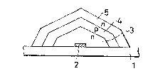
Figs. lA - lD show diagrammatically the steps for
producing a semiconductor article of the first embodiment
of the present invention.
In Fig. lA, a seed 2 formed of the nucleation surface
formi~ng material is formed by fine patterning on the
substrate 1. As the material for the substrate 1, for
example, SiO2 may be employed. The substrate 1 may be
prepared by forrning an SiO2 layer on a desired substrate
such as semiconductor, maqnetlc material, piezoelectric
~2~
- 16 - ,
I material, insulating material, etc. by the sputtering
method, the normal pressure CVD method, the vacuum vapor
deposition method, etc. As the nonnucleation surface
material, SiO2 is desirable, but SiOx with the value of
x being varied may be also available.
By depositing a silicon nitride layer (here Si3N4
layer) or a polycrystalline silicon layer as the nucleation
surface on the substrate 1 of SiO2 by the reduced pressure
vapor phase growth method, and subjecting the silicon
nitride layer to patterning by conventional lithographic
technique or lithographic technique by use of X-ray,
electron beam or ion beam, a minite substantially square
seed 2 with a thickness oE about 300 A and a size of about
1 to 4 ym is formed.
Next, as shown in Fig. lB, Si epitaxial growth is
practiced on the seed 2 by use of conventional epitaxial
growth method. At this time, by setting the production
conditions at appropriate conditions, no Si nucleus is
formed on the substrate 1 of SiO2, and an Si nucleus is
formed selectively only on the seed 2 of Si3N4.
In the present 1nventionj during the stage when
a monocrystal is formed by growing a single nucleus on
the seed 2, an impurity of desired kind and amount is
doped for a desired time to form a spec1fic conduction
type semiconductor region of~a desired kind with a desired
size and at A desired position within the monocrystal.
~he conditions for effecting selectively nucleation
:
. ., "
.
`` ~L;29~
I of Si monocrystal on the seed 2 on the substrate 1 may
be, forexample, flow rates of SiH2Cl2, HCl, H2, respectively,
of 0.6~/min., l.OQ/min. and lOOQ/min., with mixing of desired
amounts of doping gas (PH3, B2H6, etc.), a temperature
of 960C and a pressure of 150 Torr, whereby no Si nucleus
is formed on the substrate l and an Si nucleus can be
selectively formed only on the seed 2 to prepare a p-type
or n-type conduction type semiconductor crystal region
with a desired size at a desired position within the mono-
Crystal.
In this example, as shown in Fig. lB, at the initialstage of growth of the monocrystal, a doping gas of the
n-type is used to permit an n-type semiconductor crystal
region (hereinafter referred to as n-type region) 3 with
an appropriate size to grow, and then by changing over
the doping gas to the p~type, a p-type semiconductor crystal
region (hereinafter referred to as p-type region) 4 is
epitaxially grown continuously on the n-type region 3.
Further, similarly, when the p-type region 4 has reached
a certain thickness, the doping gas is changed over to
the n-type, and an n-type reglon 5 is epitaxially grown
continuously to prepare an island-shaped Si monocrystal
having n-p-n layers laminated continuously as shown in
Fig. lB.
Next, as shown in Figs. ].C and lD, by flattening
of the Si monocrystal grown in island shape at an appro-
priate level, a semiconductor article can he produced.
I The semiconductor article in this example is a truncated
cone, with the n-type Si monocrystal 3, the p-type Si
monocrystal 4 and the n-type Si monocrystal 5 being formed
in this order, as shown in Figs. lC and lD.
Typical flattening may include the lapping-polishing
method and the etch-back method.
The lapping~polishing method is a method in which
Si monocrystal is ground mechanically from the upper
part (lapping) and further the surface is subjected to
mirror surface finishing by chemical treatment and
polishing (polishing).
The etch-back method is a method in which a resist
is applied flatly to an appropriate thickness so as to
cover Si monocrystal and the resist and Si monocrystal
are etched together by RIE (Reactive-Ion-Etching~.
In the above embodiment of the process for producing
a semiconductor article, p-type, n-type and p-type layers
are laminated to form p-n-p junction, but p-n-p junction
may be formed from only p-type layer and n-type layer.
Figs. 2A - 2D show diagramatically the steps of
second embodiment of the process for producing a semi-
coaductor art~icle of the presen~t~1nvention.
In this embodiment, the same reference denotes
; the~same constituting member as in the first embodiment,
25~ and since the production process generally follows the
~same steps, the fo]lowing e~planation is focused to the
characteri~ing part making the ~ifference between the
~2968~L6
1 two embodiments.
In an example of this embodiment, as shown in
Fig. 2B, at the initial stage of growth of the monocrystal,
a doping gas of the n-type is used to permit an n-type
semiconductor crystal region (n-type region) 3 with an
appropriate size to grow, and then by changing over the
doping gas to the p--type, a p-type semiconductor crystal
region (p-type region) 4 is epitaxially grown continuously
on the n-type region 3, thereby preparing an island-shaped
Si monocrystal haivng n-p layers laminated continuously.
Next, as shown in Fig. 2C, by flattening of the
Si monocrystal grown in island shape at an appropriate
level, the monocrystal is formed in the shape of truncated
cone with the p-type region 4 being arranged outside of
the n-type region 3.
Next, as shown in Fig. 2D, the p-type region 4
is divided into two portions by use of fine working
technique to form p-type regions 4a and 4b.
Fine working technique is not particularly limited,
but work1ng can be practiced by use of the lithographic
techn1que comprising conventional reslst process and
etching process.
,
The resist process comprises the steps of resist
coat1ng, exposure, devel~oping and hard baking, and for
25~ pattern~ing of the resist, UV-ray, electron beam, X-ray,
etc. may be employed depending on the precision required.
~ lor the etch1ng p~oc~ss, both wet e-chin~ and dry
.~ ~
- - '
- 20 -
etching may be available, and it is desirable to
use a method capable of anisotropic etching such as reactive
ion etching, etc. when high precision is required.
A variety of semiconductor devices can be fabricated
by use of the semiconductor axticle produced according
to the process for producing a semiconductor article of
the present invention as described above.
The case of forming a bipolar transistor on the
semiconductor article prepared in the steps as described
above is explained below. A conventional semiconductor
production process may be employed for forming such a
bipolar transistor.
Fig. 3A illustrates a constitution of an n-p-n
type bipolar transistor by use of the semiconductor article
produced by the first embodiment of the present invention,
and Fig. 3B a constitution of a p-n-p type bipolar
transistor.
As shown in Fig. 3A, the n-p-n type bipolar
transistor has an emitter electrode ((E) in the Figure,
the same symbol is used ln the following examples) formed
ln the n-type semiconductor region at the inner side of
the semiconductor article as shown in Figs. lC and lD,
a base electrode in the p-type semiconductor region
~((B)~in the Figure, the same symbol is used in the
25~ follow~ing examples) and a collect~or electrode ((C) in
the Figure, the same symbol is used in the following
examples) in the outer n-type semiconductor region.
,
:lLZ~1~8~6
I Also, as shown in Fig. 3B, the p-n-p type bipolar
transistor, by changing the order of the doping gases
added in the monocrystal growth process, is formed
from a semiconductor aritcle with conduction types
opposite to those of the semiconductor artiele shown in
Figs. lC and lD and has an emitter electrode formed in
the inner p-type semiconductor region of the semieonduetor
artiele, a base eleetrode in the n-type semieonduetor
region and a eolleetor electrode in the outer p-type
semiconduetor region.
Fig. 4A is a constitutional illustration of the
p-n-p type bipolar transistor by use of the semieonduetor
article produced by the seeond embodiment of the present
invention.
lS As shown in Fig. 4A, the p-n-p type bipolar
transistor has a base electrode in the n-type region
arranged at the inner side of the semieonductor artiele
shown in Fig. 2D, an emitter electrode in the p-type
region 4b and a eolleetor eleetrode in the p-type region
4a.
In the above semieonduetor artiele, the outer
p-type region 4 is divided to eonstitute a p-n-p type
bipolar transistor, but it is also possible to form a
p-n-p type bipolar transistor by dividing the inner
semieonductor erystal region.
Fig. 4B lS a constitutional illustration showing
another example of the p-n-p bipo]ar transistor according
~2~
- 22 -
I to the second embodiment of the present invention.
As shown in Fig. 4B, in the monocrystal
growth process, by changing the order of doping gases
added, a semiconductor crystal region with conduction
types opposite to those of the semiconductor crystal
region shown in Fig. 2C is formed, and the inner
p-type region is divided into two p-type regions to
form a collector electrode, an emitter electrode,
respectively, and a base electrode is formed in the
outer n~type region.
As a semiconductor device for which the process
for producing the semiconductor article of the present
invention is used, other than bipolar transistor,
there can be exemplified junction type field effect
transistor, MOS type field effect transistor, rectifying
device, SCR, triac, etc.
,
~fi~
- 23 - -
1 In the following, examples in which the production
process of the present invention is used for the semi-
conductor article of such a semiconductor device are
described.
(l) Junction type field effect transistor:
Fig. 5A is a constitutional illustration of
actuation of a junction type field effect transistor, and
Figs. 5B and 5C are constitutional illustrations of
junction type field effect transistors formed according
to the present invention.
As shown in Fig. 5A, the general basic consti-
tution of a junction type field effect -transistor
comprises p-type semiconductor regions on both sidés of
the n-type semiconductor region sandwiched therebetween,
further gate electrodes t(G) in the Figure, the same
symbol is used in the respective examples shown below)
in the two p-type semiconductor regions, a source
electrode ((S) in the Figure, the same symbol is used
in the respective examples shown below) and a drain
electrode ((D) in the Figure, the same symbol is used
in the respective examples shown be1Ow) in the n-type
semiconductor region so as to be perpendicular to the
opposed gate electrodes, and by controlling the width
of the channel for electrons from the source to the
drain by the field effect of the voltage applied on
the gate, the current between the source and the drain
is controlled.
i8~i
- 2~ -
I When the junction type field effect transistor
is prepared by use of the semiconductor article produced
according to the first embodiment of the present invention,
as shown in Fig. 5B, the respective desired impurities
are doped at the stage when a monocrystal is grown to
form an n-type semiconductor region on the first p-
type semiconductor region, and further after formation
of the second p-type semiconductor region, the monocrystal
is flattened and is provided with gate electrodes in
the first p-type semiconductor region and the second
p-type semiconductor region, and a source electrode
and a drain electrode are formed in the n-type semi-
conductor region with a certain distance therebetween.
When the aforesaid junction type field effect
transistor is prepared by use of the semiconductor
article produced according to the second embodiment of
the present invention, as shown in Fig. 5C, the respective
desired impurities are doped at the stage when a mono-
crystal .is grown to form n-type and p-type semiconductor
regions, then the monocrystal is flattened and the p-type
~semiconductor region ~is devided into two p-type
~semiconductor regions followed by formation of gate
electrodes thereon respectively and of source and drain
electrodes spaced from each other by a certain distance.
(2) MOS type ~ield effect transistor:
Fig. 6A is a constitutional illustration of a
MOS type field effect translstor, and Fig. 6R is a
- 25 -
1 constitutional diagram of a junction type field effect
transistor formed by the present invention.
As shown in Fig. 6A, the general constitution
of the MOS type field effect transistor (here description
is made about the p-channel MOS type field effect
transistor) has two p-type semiconductor regions with a
certain distance therebetween in an n-type semi-
conductor substrate, and gate electrodes of Al, etc.
formed with interposing an insulating film on the
n-type semiconductor region sandwiched between these
p-type semiconductor regions. When the gate is at zero
potential, p-n junction stops current, but when a
negative potential (in the case of p-channel MOS
transistor) is applied, through its field effect, a
1~ p-channel layer is generated at the interface between
the gate oxide film and the n-type semiconductor
substrate, whereby current can be passed between the
source and the drain.
When the MOS type field effect transistor is
prepared by use of the semiconductor substrate
produced according to the present invention, the
respective desired impurities are doped ln the stage
when a monocrystal is~grown, and an n-type semlconductor
~ region is formed on the first p-type semiconductor region,
and further after formation of the second p-type semi-
conductor region thereon, the monocrystal is flattened,
and a drain electrode is formed ln the first p-type
- 26
I semiconductor region, a gate electrode in the n~type
semiconductor region and a source electrode in the
second p-type semiconductor region.
(3) SCR
Fig. 7A is a constitutional illustration of
actuation of an SCR, and Fig. 7B is a constitutional
illustration of an SCR formed according -to the present
invention.
As shown in Fig. 7A, the general constitution
of an SCR comprises a four-layer structure having p-
type semiconductor regions and n-type semiconductor
regions laminated alternately, having anode electrode
((Al in the Figure) and cathode electrode ((K) in the
Figure) formed respectively in the p-type semiconductor
region and the n-type semiconductor region at the both
ends, and a gate electrode ((G) in the Figure) in the
p-type semiconductor region sandwiched between the
both n-type semiconductor regions, and the device
functions like a diode wh1ch can control the current
passage time in the normal direction current, having
stable switching function in the two directions.
More specifically, it is a devlce capab-e of producing
the following states:
:: : : : : ~
(a) The "reverse-blocking state" when positive
Z5 voltage lS applied on the cathode;and negative voltage
on the anode. This state has nothing to do with the
gate el~ectrode.
:
- 27 - ;
1 (b) The "off state" when positive voltage is
applied on the anode, negative voltage on the cathode,
and zero or negative voltage on the gate.
(c) The "on state" when positive voltage is
applied on the gate of the SCR under off state.
When the SCR is prepared by use of the semi-
conductor article produced according to the first
embodiment of the present invention, after lamination
of the first n-type semiconductor region, the first
p-type semiconductor region, the second n-type semi-
conductor region and the second p-type semiconductor
region in this order by doping of the respective
desired impurities at the stage of growing a monocrystal,
the monocrystal is flattened, and a cathode electrode
is connected to the first n-type semiconductor region,
a gate electrode to the first p-type semiconductor
region and an anode electrode to the second p-type
semiconductor region.
(4) Triac:
Flg. 8A is a constitutional illustration of a
trlac~and Fig. 8B is a constitutional il;lustration of
the triac by use of the semiconductor article according
to the present invention. As to the preparation stèps
of the semiconductor artlcle, they are approximately
the same as those for the semiconductor article shown
in ~i(3s. lA - lD, and detailed dcscription is omitted.
Triac is a tripolar device capable of AC control.
It is equivalent to SCR arranged in reverse parallel,
,
--~ 3L2~ 6
- 28 _
1 and a signal of either positive or negative can be
given as the trigger to the gate to enable turn off.
When a triac is prepared by use of the semi-
conductor article produced according to the second
embodiment of the present invention, similarly as in
the preparation steps shown in Figs. 2A - 2D, in the
monocrystal growth process, by changing the order of
the doping gases added and laminating an n-type region,
a p-type region and an n-type region by lamination,
and thereafter flattening the island-shaped Si monocrystal
grown at an appropriate level, the Si monocrystal can
~be made a truncated cone to form an n-type region, a
p-type region and an n-type region outward in this order.
The outer n-type region and the p-type region are divided
lS into two portions, and further one of the divided n-type
regions is divided into two portions, thus forming
three n-type regions 5a, Sb and 5c and two p-type regions
4a and 4b. By forming primary electrodes ((Tl), (T2) in
the Figure) in the n-type regions 5a and 5b and a gate
electrode ((G) in the Figure) in the n-type region 5c,
a triac with a 5-layer constitution of n-p-n-p-n is formed.
(S) Rectifying device:
Fig. 9A is a constitutional illustration of
actuation of an example of a~re~ctifying element, and
~Flg. 9B a constitutional lllustra~tion of a rectifying
elenle!lt fo~mcd according to ~he present invention.
As sho~n in Fig. 9A, the basic constitution of
1~361~6
- 29 -
1 the rectifying element in this example comprises a p-
type semiconductor region and an n-type semiconductor
region on both sides with an i (intrinsic) type semi-
conductor region sandwiched therebetween, which may be
S preferably used for uses with relatively greater
consumption power.
When the rectifying element is prepared by use
of the semiconductor article produced according to the
first embodiment of the present invention, a p-type
semiconductor region is formed by doping of a p-type
impurity at the stage when a monocrystal is grown, an
i-type semiconductor region is formed thereon, further
an n-type semiconductor region is formed by doping of
an n-type impurity, followed by formation of electrodes
in the p-type semiconductor region and the n-type
semiconductor region. Of course, by omitting deposition
of the intermediate i-type semiconductor region, merely
a diode with only p-n junction may be produced.
As explained above, according to the process
for producing a semiconductor article, semiconductor
crystal regions different in characteristics can be
formed very easily at a desired thickness and position
within at least part of a semiconductor monocrystal by
varying the production conditions such as the kind and
composition ratio of deposition material, the kind and
~monrlt of impurity, etc.
In the present invention, by flattening the
- 30 -
1 protruding portion of a semiconductor monocrystal and
exposing semiconductor crystal regions different in
characteristics to form them closely next to each other
at a desired thickness and position with forming a
5 nearly right angle with reference to the substrate, the
width, depth, etc~ of a semiconductor crystal region
becomes controllable with high preclsion.
In the present invention, by forming a plurality
of semiconductor crystal regions different in charac-
teristics and then dividing at least one semiconductorcrystal region by use of fine working to form separately
semiconductor crystal regions having the same charac-
teristics simultaneously and easily with high precision,
it becomes possible to reduce the number of lamination
and simplify the process in producing a semiconductor
device comprising semiconductor crystal regions of the
same material with interposing a semiconductor crystal
region of a different material therebetween.
: