Note : Les descriptions sont présentées dans la langue officielle dans laquelle elles ont été soumises.
~ S ~J-653~
-- 1 --
FRA~AE SYNCHRONIZING APPARATUS
BACKGROUND OF THE INVE~IOM
l. Field of the Invention
The present invention relates to an apparatus
for establishing a frame synchronization of received
data, and more particularly, to a high-speed frame
synchronizing apparatus which realize a high-~peed
operation and a quick establishment of a synchroni-
zation.
In PCM communications, transmission data must
be correctly received on the receiving side. To realize
this, a frame synchronizing signal is superposed over
the transmission data, and the receiving side identifies
phases of received data according to the frame synchro-
nizing signal. Such a frame synchronization is general-
ly adopted.
In this frame synchronization, a synchronizing
operation must be carried out as quickly as possible, to
shorten the time needed for establishing a synchroni-
æation.
2. Description of the Related Art
In the conventional frame synchronization, two
methods are used, i.e., a synchronization detecting
process is carried out for every bit; or a synchroni-
zation detecting process is carried out for every frame.
In the former method, the frame synchronizing
signal can be detected within one frame period so that
the synchronization can be quickly established.
However, the operating speed of various
components in the synchronizing apparatus must be very
high, and this is a problem which the present invention
intends to solve.
In the latter method, the operating speed of
the main components in the synchronizing apparatus may
be rather low, but the frame synchronization takes a
very long time. This is another problem which the
iL29~0~;
2 --
present invention intends to solve.
SUM~R~ OF THE INVENTION
Accordingly, an embodiment of the present invention
provides a frame synchronizing apparatus in which a
synchronization is established within a short time and
the components in the apparatus can operate at a low
speed.
In accordance with an embodiment of the present
invention there is provided a frame synchronizing
apparatus in a receiving apparatus for receiving digital
signals for PCM communication, the digital signals
including serial signals at a rate of fO bits per second
(bps), the serial signals including a frame synchronizing
signal with n bits or a part of the frame synchronizing
signal, collectively arranged in one frame. The frame
synchronizing apparatus comprises: latching means for
converting the serial signals into parallel signals and
for latching the parallel signals in response to a latch
timing pulse; synchronization detecting means for
detecting the frame synchronizing signal from the
parallel signals; latch timing signal generating means
for generating the latch timing pulse at a rate of fo/k
(bps) where 1 < k <n, so that the latching means latches
the parallel signals a plurality of times while receiving
a frame of the digital signals; and phase shifting means
for changing the rate of the latch timing pulse in
response to the synchronization detecting means not
detecting the frame synchronizing signal while receiving
the frame.
In accordance with another embodiment of the present
invention there is provided a frame synchronizing
apparatus in a receiving apparatus for receiving digital
signals for PCM communication, the digital signals
including serial signals at a rate of fO bits per second
:
r
: ~
~8~1~5
(bps), the serial signals including a frame synchronizing
signal with n bits or a part of the frame synchronizing
signal collectively arranged in one frame. The frame
synchronizing apparatus comprises: latching means Eor
converting the serial signals into parallel signals and
for latching the parallel signals in response to a latch
timing pulse; synchronization detecting means for
detecting the frame synchronizing signal from the
parallel signals; and latch timing signal generating
means for providing the latch timing pulse having a
frequency of fo/k Hz, where n > k 2 2, before the
detection of the frame synchronizing signal and having a
frequency of fO/n Hz after the detection of the frame
synchronizing signal.
In accordance with a further embodiment of the
present invention there is provided a frame synchronizing
apparatus in a receiving apparatus for receiving digital
signals for PC~ communication, the digital signals
comprising serial signals at a rate of fO (bps), the
serial signals including a frame synchronizing signal
comprising n bits or a part of the same synchronizing
signal collectively arranged in one frame. The frame
synchronizing apparatus comprising: latching means for
converting the serial signals into parallel signals and
for latching the parallel signals; parallel
synchronization detecting means, having a plurality of
; synchronization detecting portions each picking up
different n bits from a one-bit-shiftad position of the
latched signal to detect the frame synchronizing signal,
comprising plural stages of synchronization detecting
portions, a synchronization control portion, and a
synchronization protection portion; and latch timing
signal generating means for providing, for the latching
means, a latch timing pulse having a frequency of fo/k
Hz, where n > k-2 2, before the detecting of the frame
~2980~1S
- 3a -
synchronizing signal and haviny a fre~uency of fO/n Hz
after the signal detection of the frame synchronizing
signal, the latch timing signal generating means
comprising a variable output counter for varying the
frequency of the latch timing pulse in accordance with a
detection of synchronization by the synchronization
detecting means; whereby when a synchronization is
detected in one of the outputs of the plural stages of
synchronous detecting portions, the synchronization
protection portion outputs a mode selecting signal for
selecting the mode of the variable output counter.
In accordance with a still further embodiment of the
present invention there is provided a frame synchronizing
apparatus in a receiving apparatus for receiving digital
signals for PCM communication, the digital signals
comprising serial signals at a rate of fO (bps), the
serial signals including a frame synchronizing signal
comprising n bits or a part of the frame synchronizing
signal, collectively arranged in one frame. The frame
synchronizing apparatus comprising: latching means for
converting the serial signals into parallel signals and
for latching (2n-1) bits of the parallel signals;
parallel synchronization detecting means, having a
plurality of synchronization detecting portions each
picking up different n bits from a one-bit-shifted
position of the latched signal to detect the frame
synchronizing signal, comprising: (2n-1) stages of
synchronization detecting portions, a synchronization
control portion, and a synchronization protecting
portion; and output selection means for extracting, from
the latched signals, a signal of one time slot at a
position corresponding to the synchronization detecting
portion which has detected the frame synchronizing signal
and outputting the extracted signal; whereby when a
synchronization is detected in one of the outputs of the
7b rr ~
.J
1~9~
- 3b
plural stages of synchronous detecting portions, the
synchroniæation protection portion outputs a mode
selecting signal for selecting the mode of the variable
output counter.
BRIEF DESCRIPTION OF THE DRAWINGS
The above features of the present invention will be
more apparent from the following description of the
preferred embodiments of the present invention, with
reference to the accompanying drawings, wherein:
Fig. 1 is a view showing a principle constitution of
a first aspect of the present invention;
Fig. 2 is a view showing a first embodiment of the
present invention;
Fig. 3 is a view showing an example of the
constitution of a variable output counter shown in Fig.
2;
Fig. 4 is a time chart showing signals of respective
portions shown in Figs. 2 and 3;
Fig. 5 is a view showing a principle constitution of
a second aspect of the present invention;
Fig. 6 is a view showing a second embodiment of the
present invention;
r ,~.~
~,
~ "
~ 4
Fig. 7 is a view showing an example of the
constitution of a variable output counter shown in
Fig. 6;
Fig. 8 is a view showing an example of the
consti~ution of a synchronization processing portion
shown in Fig. 6;
Fig. 9 is a time chart showing signals of the
respective portions shown in Figs. 7 and 8;
Fig. 10 is a view showing a third embodiment
of the present invention;
Fig. 11 is a view showing an example of the
constitution of a variable output counter with a phase
control function shown in Fig. 11;
Fig. 12 i9 a view showing a fourth embodiment
of the present invention;
Fig. 13 is a view showing a principle consti~
tution of a third aspect of the present invention;
Fig. 14 is a view showing a fifth embodiment
of the present invention;
Fig. 15 is a view showing an example of the
constitution of a synchronization processing portion
shown in Fig 14;
Fig. 16 is a time chart showing signals of the
respective portions shown in Figs. 14 and 15;
Fig. 17 is a view showing a sixth embodiment
of the present invention;
Fig. 18 is a view showing a seventh embodiment
of the present invention;
Fig. 19 is a view showing an example of the
constitution of a synchronization processing portion
shown in Fig. 18;
Fig. 20 is a time chart showing signals of the
respective portions shown in Figs. 18 and 19;
Figs. 21 and 22 are views showing other
embodiments of the present invention, respectively;
Fig. 23 is a view showing ~n example of a
frame structure;
~L2~
Fig. 24 is a view showing the constitution of
a first prior art;
Fig. 25 is a time chart showing signals of the
respective portions of the prior art example shown in
Fig. 24;
Fig. 26 is a view showing the constitution of
a second prior art; and
Fig. 27 is a time chart showing signals of the
respective portions of the prior art example shown in
]0 Fig. 26.
DESCRIPTION OF THE PREFERRED EMBODIMENTS
For a better understanding of the present in-
vention, a conventional frame synchronizing apparatus
will first be described.
Throughout the description, the same or similar
portions are represented by the same or similar refer-
ence symbols.
Two methods to be described hereunder are used in
prior art frame synchronization systems, and in the
following description, it is assumed that, as shown in
Fig. 23, one frame consists of m time slots (TSs) and
one time slot consists of n bits. Further, a frame
synchroniæing signal FSYNC is collectively arranged in
the first time slot.
Figure 24 is a view showing the constitution of a
first prior art example in which a synchronization
detecting process is carried out for every bit, and
Fig. 25 is a time chart showing signals of the respec-
tive portions of the prior art example.
~30 In Fig. 24, input serial data at a rate of f0 bps
is converted by a serial-to-parallel (S/P) converting
portion l with clocks having a frequency of f0 Hz into
parallel signals each of n bits corresponding to one
time slot. The converted signals are latched by a latch
; 35 portion 2 with clocks of f0 Hz and fO/n Hz to generate
output data of fO/n bps.
On the other hand, a synchronization detecting
-- 6
portion 5 eompares the parallel signal of n bits sup-
plied by the serial-to-parallel converting portion 1
with a predetermined frame synchronizing signal pattern
and, if they coincide, generates a reset signal to reset
counters 3 and 4. The counter 3 is a bit counter for
eounting the number of bits of the input data with
elocks of fO Hz to generate pulses of fO/n bps to
delimit the time slots. The counter 4 is a time slot
eounter for counting the fO/n pulses of the counter 3 to
generate pulses of fO/nm bps to delimit the frames.
A synchronization protecting portion 8 cheeks, in
response to outputs of the eounter 4, whether or not the
synchronization detecting portion 5 again deteets a
eoineidence when the next frame synchroniæation signal
arrives. As a baekward synehronization proteetion, the
above operation is repeated several times, and when the
frame synehronizing signal pattern is eonsecutively
detected a predetermined number of times, a frame
synehronization is established to output a frame syn-
ehronous pulse F.Syne.
Figure 25 shows that, when a frame synehronoussignal pattern of Fl, ..., Fn-l and Fn illustrated by an
enclosed rectangle appears in the register outputs SRl,
..., SRn-l and SRn in the serial-to-parallel converting
portion l, a reset signal is output to reset the
counters 3 and 4.
Figure 26 shows a second prior art example in which
the synchronous detection proeess is earried out for
every time slot, and Fig. 27 is a time ehart showing
signals of the respective portions of the above example.
In Fig. 26, a serial-to-parallel converting
portion lj a latch 2 and a counter 3 constitute a
high-speed portion. Input serial data at a rate of
O bps is eonverted by the serial-to-parallel converting
portion l with eloeks of fO Hz into parallel signals
eaeh of n bits eorresponding to one time slot. The
parallel signals are latehed in the lateh 2 with eloeks
129800~i
-- 7
of f0 Hz and fO/n Hz of the counter 3 to generate output
data of fO/n bps. The counter 3 is a high-speed counter
for counting the number of bits of the input data with
clocks of f0 Hz to generate pulses of fO/n bps to
delimit time slots.
On the other hand, a detection portion 7, a
counter 8, and a synchronization protecting portion 9
constitute a low-speed portion. The synchronization
detecting portion 7 compares the parallel signal of n
bits latched by the latch portion 2 with a predetermined
frame synchronizing signal pattern to detect whether or
not they coincide.
When the synchronization detecting portion 7 does
not detect a coincidence, the synchronization protecting
portion 9 sends a shift pulse to the counter 3 to shift
a count by one bit such that a latch timing in the latch
portion 2 is shifted by one bit. The synchronization
detecting portion 7 then performs the coincidence
detection process for the next frame. This operation is
repeated, and the latch timing is successively shifted
by one bit to continue the synchronous detection. When
the synchronization detecting portion 7 detects a
coincidence with the frame synchronization signal
pattern, the synchronization protecting portion 9
generates a reset signal to reset the counter 8. The
counter 8 is a low-speed counter for counting the number
of pulses of fO/n of the counter 3 to generate pulses of
fO/nm bps to delimit frames.
Subsequently, as a back protection, a check is made
to determine whether or not a coincidence is repeatedly
detected a plurality of times, and if the frame synchro-
nization signal pattern is consecutively detected a prede-
termined number of times, it is judged that a frame
synchronization has been established and a frame syn-
chronous pulse F.Sync is output.
In Fig. 27, respective register outputs LRl, ....LRn-l and LRn of the latch portion 2 are sequentially
~298~
-- 8
shifted by one bit according to shift pulses. When a
frame synchronizing cignal pattern of Fl, ..., Fn-l and
Fn appears as illustrated by an enclosed rectan~le, a
reset signal is output to reset the counter 8.
In the first prior art example shown in Figs. 24
and 25, the frame synchronizing signal is detected at
the transmission speed (fO bps) by the synchronization
detecting portion, and if there is no error in the
transmission signals, the frame synchronizing signal
can be easily caught within one frame period so that the
synchronization can be quickly established.
~ owever, in the first example, the processes of
serial-to-parallel conversion, synchronous deteotion,
and counter reset must be completed within one bit so
that the respective components must operate at a high
speed. Since the apparatus shown in Fig. 24 includes a
loop which requires a high-speed operation, it is
presumed that an operable speed of devices used (partic-
ularly flip-flops) other than the devices in the loop is
half or lower than the maximum operating speed.
In the second prior art example shown in Figs. 26
and 27, components which need a high-speed operation are
only the serial-to-parallel converting portion l, latch
portion 2, and counter 3, which constitute a high-speed
portion. A low-speed portion including a loop system
may operate at a time slot speed so that an operable
speed of the system with respect to the maximum opera-
tion speed of devices used is improved.
However, in this system, it takes a long time to
detect the frame synchronizing signal. In the worst
case, a time period of n frames is required, and thus it
takes a long time to establish a synchronization.
Therefore, when transmission lines are switched,
terminal devices are seriously affected. This will be a
particular problem when these devices are connected in
multiple stages.
The present invention is intended to solve the
129800~;
problems of the prior art techniques.
Figure 1 is a view showing a principle constitution
of a first aspect of the present invention. In Fig. 1,
the principle constitution of a frame synchronizing
apparatus is shown. The frame synchronizing apparatus
is provided at the receiving side of a PCM communication
system, in which frames each including a frame synchro-
nizing signal of n bits or a part thereof collectively
arranged in the frame are serially transmitted at a rate
of f0 (bps). The system comprises a latching means 101,
a synchronization detecting means 102, and a latch
timing signal generating means 103.
In the operation of the frame synchronizing appara-
tus shown in Fig. 1, input serial data is converted for
lS every n bits with clocks of f0 Hz by a serial~to-
parallel converting portion in the latching means 101
into paralle~ outputs each of n bits. Before the
detection of the frame synchronizing signal, the paral-
lel outputs are latched for every n bits with latching
pulses of fO/n Hz by the latching means 101. One
synchronization detecting portion is provided in the
synchronization detecting means 102 to detect the frame
synchronizing signal in the latched data at a latching
cycle of Tk = k/fo. If not detected, the latching
pulses are shifted by one bit for every frame to shift
the latched data by one bit to detect the frame synchro-
nizing signal, and thus the frame synchronizing signal
is detected within k frames. After the detection of the
frame synchronizing signal, the latching pulse~ are
changed to fO/n ~z to repeat the detection with a
latching cycle of Tn = n/fO. If there is no trans-
mission error, the synchronization detection is made for
every frame. If the frame synchronizing signals are
detected a predetermined number of times, it is judged
that a synchronization has been established.
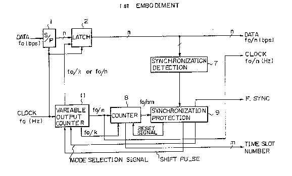
Figure 2 is a view showing a first embodiment
derived from the first aspect of the present invention
129800~;
-- 10 --
shown in Fig. 1. In the figure, the same parts as those
shown in Fig. 26 are represented by like numerals, and a
numeral 11 represents a variable output counter.
Figure 3 is a view showing an example of the
arrangement of the variable output counter 11 shown in
Fig. 2, and Fig. 4 is a time chart showing signals of
respective portions shown in Figs. 2 and 3. In the
figure, it is assumed that n = 4 and k = 2.
A serial-to-parallel (S/P) converting portion 1, a
latch portion 2, and the variable output counter 11
constitute a high-speed portion which is the same as
that shown in Fig. 26. However, the variable output
counter 11 divides clocks of fO Hz to senerate two
different divided frequencies (fo/k Hz and fO/n Hz).
The frequency dividing ratio k is set as n ~ k > 2.
Input serial data of fO bps is converted by the
serial-to-parallel converting portion 1 with clocks of
fO Hz into parallel signals each of n bits corresponding
to one time slot, and latched by the latching portion 2
with clocks of fO ~z and those of the variable output
counter 11 to generate output data.
Before a synchronization detecting portion 7
detects a frame synchronizing signal, the variable
output counter 11 generates divided outputs of fo/k
according to a mode selection signal from a synchroni-
zation protecting circuit 9. With the divided outputs,
the latch portion 2 latches the input data to generate
output data each of n bits.
The synchronization detecting portion 7, a coun-
ter 8 and the synchronization protecting portion 9constitute a low-speed portion. The synchronization
detecting portion 7 compares the parallel signal of n
bits latched by the latch portion 2 with a predetermined
frame synchronizing signal pattern to detect whether or
not they coincide. In this case, the detection of the
frame synchronizing signal is carried out for every k
bits of the input data.
1298005
-- 11 --
If the synchronization detecting portion 7 does not
detect a coincidence in one frame period, the synchroni-
zation protecting portion ~ sends a shift pulse to the
variable output counter ll to shift a count by one bit,
thereby shifting a latch timing of the latch portion 2
by one bit. The synchronization detecting portion 7
again carries out the coincidence detection. This
operation is repeated such that the synchronization
detection is continued while the latch timing is succes-
sively shifted by one bit. Therefore, if there is notransmission error, a coincidence will be detected
within k frames at the worst. If k = 2, for example/
the coincidence is always detected in the next frame.
If the synchronization detecting portion 7 detects
a coincidence with the frame synchronization signal
pattern, the synchronization protecting portion 9
generates a mode selection signal to cause the variable
output counter 11 to yenerate a frequency-divided output
having a frequency of fO/n. Accordingly, the latching
portion 2 latches input data for every time slot, and a
reset signal is generated to reset the counter 8. The
counter 8 is a low speed counter for counting pulses of
f~/n of the variable output counter 11 to generate
pulses of fO/nm bps to delimit frames.
Subsequently, the synchronization detection is
carried out for every frame. As a backward synchro-
nization protection, a checked is made to determine
whether or not a coincidence is detected a plural number
of times and, if the frame synchronizing signal pattern
is consecutively detected a predetermined number of
times, it is judged that frame synchronization has been
established to output a frame synchronous pulse F.Sync.
As shown in Fig. 3, the variable output counter ll
comprises a first stage counter CNTl and a second stage
counter CNT2 for counting clocks having a frequency of
fO. The counter CNTl generates clocks of fo/k~ and the
counter CNT2 generates clocks of fO/n. When n = 4 and k
i298005
= 2, the counter CNTl is a 1/2 frequency dividing
counter, and the counter CNT2 is a 1/4 frequency dividing
counter. According to mode selection signals of the
synchronization protecting portion 9, a selector SEL
selects clocks of the counter CNTl or CNT2 and outputc
the selected clocks. By applying a shift pulse to a
count enable terminal EN of the counter CNTl, the count
is shifted.
In Fig. 4, corresponding to n = 4, each of the
serial-to-parallel converting portion 1 and latch
portion 2 is constituted by four bits. When the frame
synchronizing signal pattern does not appear on regis-
ters SRl, SR2, SR3, and SR4 of the serial-to-parallel
converting portion 1, the mode selection signal is "L"
and the latching cycle is Tk = k/fo (sec). By shifting
a count of the variable output counter 11 according to a
shift pulse, the contents of ~-he respective registers
are sequentially shifted by one bit and latched by the
latch portion 2 with latch clocks of fo/k~ When the
frame synchronizing signal pattern of Fl, F2, F3, and F4
appears as illustrated by an enclosed rectangle, syn-
chronization is detected so that the mode selection
signal is changed to "H". Then the data is latched with
latch clocks of fo/k~ and the latch cycle becomes Tn
= n/fO (sec). A reset signal is output to reset the
counter ~.
According to the embodiment shown in Fi~s. 2 to 4,
the synchronization detection is carried out at a high
speed before the detection of the frame synchronizing
signal with latchiny cycles of fo/k (k < n) so that a
worst synchronization detection time is shortened to
Tmax = kTf (Tf being frame cycles~ (2 _ k < n). If an
operation speed of the frame processing portion is made
to be half lcorresponding to k = 2) of a transmission
speed, considering the total balance of a frame synchro-
nization circuit, a synchronization detection time
period which was n frames in the prior art example shown
129800S
in Fig. 27, is shortened to two frames. On the other
hand, after the detection of the frame synchronizing
signal, the synchronization establishing process is
carried out at a low speed of fO/n. Thus, a high-speed
operation and a short synchronization establishing time
can be simultaneously realized.
Figure 5 is a view showing a principle constitution
of a second aspect of the present invention. In Fig. 5,
the principle constitution of a frame synchronizing
apparatus is shown. The frame synchronizing apparatus
is provided at the receiving side of a PCM communication
system in which Erames each including a frame synchro-
nizing signal of n bits or part thereof collectively
arranged in the frame are serially transmitted at a rate
of f0 (bps). The apparatus comprises a latching
means 101, a parallel synchronization detecting
means 102A and an output selection means 104.
The latching means 101 converts input serial
signals into parallel signals and latches the parallel
signals.
The synchronization detecting means 102 detects the
frame synchronous signal in the latched signals.
The parallel synchronization detecting means 102A
has a plurality of synchronization detecting portions
each sequentially picking up different n bits from a
one-bit-shifted position of the latched signals to
detect the frame synchronizing signal.
The latch timing signal generating means 103
provides, for the latching means 101, latch timing
pulses of fo/k (Hz) (n > k _ 2) before the detection of
the frame synchronizing signal and of fO/n (Hz) after
the detection of the frame synchronizing signal.
The output selection means 104 extracts signals
among the latched signals in one time slot at positions
corresponding to the synchronization detecting portion
from which the synchronizing signal has been detected,
and outputs the extracted signals.
i291~
- 14 -
According to the second aspect of the present
invention shown in Fig. 5, the output selection
means 104 may be a selector means for selecting signals
out of a plurality of output lines of the latching
means 101 in one time slot according to the control of
the parallel synchronization detecting means 102A which
has detected the frame synchronizing signal, or the
output selection means 104 may be a phase selection
means for changing the phase of a latch timing pulse of
the latch timing signal generating means 103 according
to the control of the parallel synchronization detecting
means 102A which has detected the frame synchronizing
signal.
In the operation of the frame synchronizing appara-
tus shown in Fig. 5, input serial data is converted for
every (n + k - 1) bits with clocks of fO Hz by a serial-
to-parallel converting portion in the latching means 101
into parallel outputs each of (n + k - 1) bits. Before
the detection of the frame synchronizing signal, the
parallel outputs are latched for every (n + k - 1) bits
with latching pulses of fo/k Hz by the latching portion.
There are k pieces of synchronization detecting portions
to detect the frame synchronizing signal in the latched
data at a latch cycle of Tk = k/fo so that synchroni-
zation can be detected within one frame. After thedetection of the frame synchronizing signal, the fre-
quency of the latching pulse is changed to fO/n Hz to
repeat the detection with a latching cycle of Tn = n1fO.
If there is no transmission error, the synchronization
detection is made for every frame. If synchronization
is detected a predetermined number of times, it is
judged that a synchronization has been established.
Among the parallel outputs of (n + k + 1) bits in the
latching portion, n bits corresponding to a number of
the synchronization detecting portion of the k pieces of
the synchronization detecting portion which has detected
the frarne synchronizing signal, are extracted to gener-
1298005
- 15 -
ate outputs for a required one time slot.
Figure 6 is a view showing a second embodiment of
the present invention based on the principle constitu-
tion shown in Fig. 5. In the figure, the same parts as
those shown in Fig. 2 are represented by like numerals,
and a numeral 11 represents a variable output counter,
12 a parallel synchronization detecting portion, 13 a
synchronization control portion, and 14 a selector.
Figure 7 is a view showing an example of the
arrangement of the variable output counter 11 shown in
Fig. 6; Fig. 8 is a view showing an example of the
arrangement of a synchronization processing portion
including a counter 8, a synchronization protecting
portion 9, the parallel synchronization detecting
portion 12, and the synchronization control portion 13
which are shown in Fig. 6; and, Figure 9 is a time chart
showing signals of respective portions shown in Figs. 6
and 7. In the figure, it is assumed that n = 4 and k
= 2.
A serial-to-parallel (S/P) converting portion 1, a
latching portion 2, and the variabl~ output counter 11
constitute a high-speed portion which is the same as
that shown in Fig. 26. However, each of the serial-to-
parallel converting portion 1 and latching portion 2 is
constituted by (n ~ k - 1) bits. Input data of fO bps is
converted with clocks of fO Hz and latched with clocks
of fO Hz and those of the variable output counter 11 to
generate output data each of (n + k - 1) bits. The
variable output counter 11 has the same constitution as
that explained with reference to Figs. 2 and 3 but does
not shift counts and thus has no shift pulse input.
Before a synchronization detecting portion 7
detects a frame synchronization signal, the variable
output counter 11 generates divided outputs of fo/k
according to a mode selection signal from this synchro-
nization protecting circuit 9. With the divided
outputs, the latch portion 2 latches the input data to
~zg80~5
- 16 -
qenerate output data each of (n + k - 1) bits.
The details of the parallel synchronization detect-
ing portion 12 are shown in Fig. 8, and comprises k
pieces of n-bit synchronization detecting portions ~1
to #k. Each of the synchronization detecting portions
sequentially picks up a signal of n bits from a one-bit-
shifted position of the parallel signals each of (n
+ k - 1) bits, and sequentially compares the signal with
a predetermined frame synchronizing signal pattern.
When any one of the synchronization detecting portions
detects a coincidence, a coincidence pulse is generated.
If the parallel synchronization detecting por-
tion 12 detects a coincidence with the frame synchroni-
zation signal pattern, the synchronization protecting
portion 9 generates the mode selection signal to cause
the variable output counter 11 to generate frequency
divided outputs of fO/n so that data is latched for
every time slot by the latching portion 2.
In the synchronization control portion 13, an OR
circuit OR operates a logical add of coincidence pulses
of the k pieces of the synchronization detecting
portions to generate a reset signal to reset the
counter 8. Also, a strobe signal is generated to write
a number of the synchronization detecting portion which
has generated the coincidence pulse into a control
memory MEM. The counter 8 is a low-speed counter to
count pulses of fO/n of the variable output counter 11
to generate pulses of fO/nm bps to delimit frames.
The synchronization protecting portion 9 responds
to an output of the counter 8 and, when the next frame
synchronizing signal is detected, determines whether or
not the parallel synchronization detecting portion 12
again detects a coincidence. At this time, a selector
SEL is controlled by an output of the control memory MEM
to select an output of the synchronization detecting
portion which has previously detected a coincidence so
that the coincidence detection process can be carried
- 17 -
out for the same time slot. This operation is repeated
several times as a backward protection in the synchroni-
zation protecting portion 9. When the frame synchroni-
zation signal pattern is consecutively detected a
cj predetermined number of times, it is judged that a frame
synchronization has been established on a frame synchro-
nous pulse F.Sync is output.
At the same time, the synchronization control
portion 13 controls the selector 14 according to the
output of the control memory MEM to select n pieces of
signals out of n + k - l lines of parallel signal
outputs of the latch portion 2 corresponding to the
synchronization detecting portion which has detected a
coincidence in the parallel synchronization detecting
portion 12. Accordingly, the selector 14 generates
output data of fO/n bps.
In Fig. 9, corresponding to n = 4 and k = 2, each
of the serial-to-parallel converting portion l and latch
portion 2 is constituted by five bits. When the frame
synchronizing signal pattern does not appear on the
registers SRl, SR2, SR3, and SR4 of the s~rial-to-
parallel converting portion l, the mode selection signal
is "L" so that the latch cycle is Tk = k/fo (sec). The
contents of the respective registers are sequentially
shifted by one bit and latched by the latching portion 2
with latch clocks of fo/k~ When the frame synchronizing
signal pattern of Fl, F2, F3, and F4 appears as illus-
trated by an enclosed rectangle, a synchronization is
detected to change the mode selection signal to "H".
Then, the data is latched with latch clocks of fO/n so
that the latch cycles become Tn = n/fO (sec), and a
reset signal is output to reset the counter 8. At the
same time, a number (l, 0) of the synchronization
detecting portion is written in the control memory MEM
by a strobe signal. Accordingly, the selector 14
selects outputs of the registers LRl to LR4 of the
latching portion 2 and outputs same.
129800$
- 18 -
According to the apparatus shown in Figs. 6 to 8,
the latching is carried out with a cycle of fo/k (k < n)
before the detection of the frame synchronizing signal
to perform the synchronization detection at a high
speed. In addition, the k pieces of synchronization
detecting portions perform the synchronization detecting
process in parallel so that the synchronizing signal can
be detected within one frame to realize a synchroniza-
tion establishing time equal to that of the first prior
art example shown in Fig. 12. On the other hand, after
the detection of the frame synchronizing signal, the
synchronization establishing process is executed with a
cycle of fO/n, and therefore, a high-speed operation and
a short synchronization establishing time are realized
simultaneously.
After the detection of the synchronization signal,
the selector 14 inserted to an output stage is con-
trolled based on the number of the synchronization
detecting portion, which has detected the synchronizing
signal and written in the control memory, among the
parallel synchronization processing portions to obtain
output data for a required one time slot.
In this second embodiment, as k becomes larger, an
operation speed of the synchronization establishment
processing portion may be lowered. Here, the number of
the synchronization detecting portions must be in-
creased.
Figure 10 is a view showing a third embodiment of
the present invention based on the second aspect shown
in Fig. 5. In the figure, the same parts as those shown
in Fig. 7 are represented by like numerals, and a
numeral 15 is a variable output counter with phase
control function. In Fig. 10, the constitution of a
synchronization processing portion including a coun-
ter 8, a synchronization protecting portion 9, a paral-
lel synchronization detecting portion 12, and a synchro-
nization control portion 13 are the same as those shown
129800~;
- 19 -
in Fig. ~.
Figure 11 is a view showing an example of the
constitution of the variable output counter 15 with
phase control function of the embodiment of Fig. 10.
In Figs. 10 and 11, when the parallel synchroniza-
tion detecting portion 12 detects a frame synchronizing
signal, a number of the synchronization detecting
portion which has detected the frame synchronizing
signal is written in a control memory MEM. Based on a
phase selection signal corresponding to the stored
number from the control memory MEM, a phase selector
Phase SE~ selects output phases of ~ 1 to ~ k of a
counter CNT2. Accordingly, among latch timing pulses of
fO/n of k lines having different phases respectively, a
pulse corresponding to the synchronization detecting
portion which has detected the frame synchronizing signal
is given to the latching portion 2. Therefore, out of n
lines of outputs of the latching portion 2, output data
is provided for a required one time slot corresponding
to the synchronization detecting portion which has
detected the frame synchronizing signal.
Figure 12 is a view showing a fourth embodiment of
the present invention based on the second aspect shown
in Fig. 5. In the figure, the same parts as those shown
in Fig. 10 are represented by like numerals, and a
numeral 16 is a shift pulse generating circuit. In
Fig. 12, the constitution of a synchronization
processing portion including a counter 8, a synchroniza-
tion protecting portion 9, a parallel synchronization
detecting portion 12, and a synchronization control
portion 13 is the same as that shown in Fig. 8.
In Fig. 12, when the parallel synchronization
detecting portion 12 detects a frame synchronizing
signal, a number of the synchronization detecting
3s portion which has detected the frame synchronizing
signal is written in a control memory MEM. According to
the embodiment shown in Fig. 12, instead of changing the
~29800S
.~ U
phase of an output clock of f /n of the variable output
counter 15 by the phase selector Phase SEL as in the
embodiment shown in Fig. lû, a shift pulse generating
portion 16 controlled by a control output of the syn-
chronization control portion 13 is provided. Accordingto an output pulse of the shift pulse generating
portion 16, the count of a variable output counter 15 is
shifted to control a latch timing of the latching
portion 2 to realize the same operation as that of the
embodiment shown in Fig. 10.
Figure 13 is a view showing a principle constitu-
tion of a third aspect of the present invention. The
frame synchronizing apparatus shown in Fig. 13 is
provided at the receiving side of a PCM communication
system in which frames each including a frame synchro-
nizing signal of n bits or a part thereof collectively
arranged in the frame are serially transmitted. The
apparatus shown in Fig. 13 comprises a latching
means lOlB, a parallel synchronization detecting
means 102B, and an output selection means 104B.
The latching means lOlB converts input serial
signals into parallel signals and latches the parallel
signals.
The parallel synchronization detecting means 102B
has a plurality of synchronization detecting portions
each sequentially picking up different n bits from a
one-bit-shifted position of the signal latched by the
latching means lOlB to detect the frame synchronizing
signal.
The output selection means 104B eY.tracts signals
among the signals latched by the latching means lOlB in
one time slot at positions corresponding to the synchro-
nization detecting portion from which the synchronizing
signal has been detected, and outputs the extracted
signals.
The output selection means 104B may be a selector
means for selecting signals out of a plurality of output
129800S
- 21 -
iines of the latching means lOlB in one time slot
according to the control of the synchronization detect-
ing portion which has detected the frame synchronous
signal, or the output selection ~eans 104B may be a
clock phase selection means for changing a latch timing
of the latching means lOlB according to the control of
the synchronization detecting portion which has detected
the frame synchronous signal.
In the operation of the apparatus shown in Fig. 13,
2n-l bits are latched at a single latch timing, and a
parallel process i5 carried out by n pieces of synchro-
nization detecting portions to detect a frame synchro-
nizing signal among n-bit signals sequentially shifted
by one bit. Thus, the frame synchronizing signal can be
detected within one frame.
The number of the synchronization detecting portion
which has detected the frame synchronizing signal, among
the n pieces of synchronization detecting portions, is
stored in a memory, and accordingly, the output selec-
tion means 104B is controlled to extract signals in onetime slot out of 2n-l pieces of data output to obtain
an output with a required frame synchronization.
Alternatively, the selector may control, by using
the number of the synchronization detecting portion
which has detected the synchronization and stored in the
memory, the phase of a latch timing pulse to obtain an
output with the required frame synchronization.
Again alternatively, and based on the number of the
synchronization detecting portion which has detected the
synchronization and stored in the memory, counts of a
counter for generating a latch timing pulse may be
shifted to control the phase of the latch timing pulse
so as to obtain outputs with the required frame synchro-
nization.
According to the arrangement of shown in Fig. 13, a
high-speed portion does not have a loop system and thus
the problem of a delay time does not occur. Therefore,
~2980()5
- 22 -
the system can be operated close to the ma~imum operat-
ing speed of the devices used.
On the other hand, the frame synchronization
detecting portion having a loop system will be operated
at a speed of l/n and not affected by the maximum operat-
ing speed of the devices used. Further, the frame
synchronization establishing time can be shortened by
the parallel frame synchronous detecting operation.
Figure 14 is a view showing a fifth embodiment of
the present invention based on the third aspect shown in
Fig. 13. In the figure, the same parts as those shown
in Fig. 26 are represented by like numerals, and numeral
12a represents a parallel synchronization detecting
portion, 13a a synchronization control portion, and 14a
a selector.
Figure 15 is a view showing an example of the
arrangement of a synchronization processing portion
including a counter 8, a synchronization protecting
portion 9, the parallel synchronization detecting
portion 12a, and the synchronization control portion 13a
shown in Fig. 14, and Fig. 16 is a time chart showing
signals of respective portions shown in Figs. 14 and 15.
In the figure, the number of bits constituting one time
slot is, for example, three.
A serial-to-parallel conve~ting portion 1, a
latching portion 2, and a counter 3 constitute a high-
speed portion which is the same as that shown in
Fig. 27. However, each of the serial-to-parallel
converting portion 1 and latching portion 2 comprises
2n-1 bits. Input data of f0 bps is converted with
clocks of f0 Hz into parallel signals and cyclically
latched with time-slot cycles with clocks of f0 Hz and
fO/n Hz to generate parallel outputs each of 2n-1 bits.
The details of the parallel synchronization detect-
ing portion 12a are shown in Fig. 15, and consists ofn pieces of synchronization detecting portions ~1 to ~n
each having n bits. Each of the synchronization detect-
129BOOS
- 23 -
ing portions sequentially picks up a signal of n bits
from a one-bit-shifted position of the parailel signals
each of 2n-1 bits, and sequentially compares the signal
with a predetermined frame synchronizing signal pattern.
When any one of the synchronization detecting portions
detects a coincidence, a coincidence pulse is generated.
In the synchronization control portion 13a, an OR
circuit OR operates a logical sum of coincidence pulses
of the n pieces of synchronization detecting portions to
generate an output to reset the counter 8. Also, a
strobe signal is generated to write a number of the
synchronization detecting portion which has generated
the coincidence pulse into a control memory MEM.
The synchronization protecting portion 9 responds
to an output of the counter 8 and, when the next frame
synchronizing signal is detected, determines whether or
not the parallel synchronization detecting portion 12a
again detects a coincidence. At this time, a selector
SEL is controlled by an output of the control memory MEM
to select outputs of the synchronization detecting
portion which has previously detected a coincidence so
that the coincidence detection process can be carried
out for the same time slot. This operation is repeated
several times as a backward protection in the synchro-
nization protecting portion 9. ~hen the frame synchro-
nizing signal pattern is consecuti~ely detected a
predetermined number of times, it is judged that frame
synchronization has been established and a frame syn-
chronizing pulse F.Sync is output.
At the same time, the synchronization control
portion 13a controls the selector 14a according to the
output of the control memory MEM to select n pieces of
signals out of 2n-1 pieces of parallel signal outputs of
the latching portion 2 corresponding to the synchroni-
zation detecting portion which has detected a coinci-
dence in the parallel synchronization detecting
portion 11. Accordingly, the selector 13 generates
~298005
- 24 -
output data of fO/n bps.
In Fig. 16, corresponding to n = 3, each of the
serial-to-parallel converting portion 1 and latching
portion 2 is constituted by five bits. A frame synchro-
5 nizing signal pattern of Fl, F2, and F3 of registers LR2
to LR4 of the latching portion 2 is detected by the
synchronization detecting portion #2, and as a result,
the counter 8 is reset, and a number ~0, 1, 0) of the
synchronization detecting portion is written in the
10 control memory MEM by a strobe signal. Accordingly, the
selector 14a selects outputs of the registers LRl to LR3
of the latching portion 2 and outputs same.
According to the apparatus shown in Figs. 14 to 16,
the parallel synchronization detecting portion is
15 effective from a free running state up to a time when
the frame synchronizing signal is first detected. If
there is no transmission error, the frame synchronizing
signal is always detected within one frame so that a
synchronization establishing time can be shortened.
20 After the detection of the synchronizing signal, a time
slot in which the frame synchronizing signal exists in
latched signals is known because it is designated by the
control memory MEM. Therefore, it is possible to
extract n pieces of necessary data outputs among the
25 2n-1 pieces of parallel signals.
Although one time slot consists of n bits and the
frame synchronizing signal also consists of n bits in
this embodiment, the frame synchronizing signal may
alternatively consist of n' bits and the number of
30 synchronous detection signal lines may be 2n'-1 to
obtain the same result with the following definitions:
if 2n'-1 < n, then the number of latches f
is n; and
if 2n'-1 _ n, then the number of latches is
2n'-1. 1 -
Figure 17 is a view showing a sixth embodiment ofthe present invention based on the third aspect shown in
1298005
- 25 -
Fig. 13. In the figure, the same parts as those shown
in Fig. 14 are represented by like numerals, and
numerals 2A and 2B represent latching portions each
comprising n bits, and 2C a selector. According to the
embodiment shown in Fig. 17, a serial-to-parallel
converting portion 1 outputs n bits for which the
latching portions 2A and 2B each storing n bits are
disposed in parallel to alternately latch n bits in
response clocks ~ 1 and ~ 2 of fO/2n from a counter 3.
By reading outputs of the latch portions 2A and 2B
alternately through the selector 2C in response to the
clock of fO/n from the counter 3, parallel outputs each
of 2n-1 bits are generated. The processes followed are
the same as those shown in Fig. 14, and a frame synchro-
nizing operation can be realized in the same manner.
Figure 18 is a view showing a seventh embodimentbased on the third aspect of the present invention. In
the figure, the same parts as those shown in Fig. 14 are
represented by like symbols, and a numeral 15 is a
selector.
Figure lg is a view showing an example of the
constitution of the synchronizztion processing portion
including the counter 8, the synchronization protecting
portion 9, the parallel synchronization detecting
portion 12a, and the synchronization control por-
tion 13b, which are shown in Fig. 18, and Fig. 20 is a
time chart showing signals of respective portions shown
in Figs. 6 and 7 and showing an example in which one
time slot consists of n = 3 bits.
The high-speed portion includes the serial-to-
parallel converting portion 1, the latching portion 2
and the counter 3, similar to the constitution of
Fig. 14. The difference between Fig. 14 and Fig. 18 is
that the phase of a latch timing signal of fO/n Hz given
by the counter 3 to the latching portion 2 in Fig. 14 is
changed from ~ 1 to ~ n by the selector 15 in Fig. 18.
The serial-to-parallel converting portion 1 converts
12~S
- 26 -
input data of f0 bps with clocks of f0 Hz into parallel
signals. The latching portion 2 latches outputs of the
serial-to-parallel converting portion 1 with a period of
the time slot in response to the clocks of f0 Hz and
fO/n Hz output from the selector 15 to generate parallel
outputs each of 2n-1 bits.
The parallel synchronization detecting portion 12a
has the same constitution as that of the embodiment
shown in Fig. 14 and comprises n pieces of synchroni-
zation detecting portions #1 to #n each of n bits. Eachof the synchronization detecting portions sequentially
picks up a signal of n bits from a one-bit-shifted
position of the parallel signals each of 2n-1 bits, and
sequentially compares the signal with a predetermined
frame synchronizing signal pattern to generate a coinci-
dence pulse when any one of the synchronization detect-
ing portion detects a coincidence.
An OR circuit OR in a synchronization control
portion 13b operates a logical sum of coincidence pulses
of the n pieces of synchronization detecting portions to
generate an output to reset the counter 8. At the same
time, a strobe signal is generated to store the number
of the synchronization detecting portion which has
generated the coincidence pulse into a control memo-
ry MEM.
The synchronization protecting portion 9 respondsto an output of the counter 8, and, when the next frame
synchronization signal is detected, determines whether
or not the parallel synchronization detecting por-
tion 12a again detects a coincidence. At this time, theselector 15 is controlled by a selector control output
from the memory MEM to generate a latch pulse in a time
slot at which the previous coincidence has been detect-
ed. This latch timing signal is given to, for example,
a first synchronization detecting portion #1, and
subsequently, the synchronization detecting portion ~1
detects the frame synchronization signal.
1298005
-- ?7 -
The synchronization protecting portion 9 checks the
synchronization detecting portion ~l to determine, as a
backward protection, whether or not a synchronization is
detected a plural number of times. When the frame
5 synchronizing signal pattern is consecutively detected a
predetermined number of times, a frame synchronization
is established and a frame synchronous pulse F.Sync is
output.
From the 2n-l pieces of parallel signal lines of
the latching portion 2, n pieces corresponding to the
synchronization detecting portion #l in the parallel
synchronization detecting portion ll are extracted to
generate output data of fO/n bps.
In Fig. 20, corresponding to n = 3, each of the
serial-to-parallel converting portion l and latch
portion 2 is constituted by 5 bits. The synchronization
detecting portion ~2 detects a frame synchronizing
signal pattern of Fl, F2 and F3 of registers LR2 to LR4
of the latch portion 2 to reset the counter 8. At the
same time, according to a strobe signal, a number (0,
1, 0) of the synchronization detecting portion is
written in the control memory MEM. Accordingly, the
selector 15 controls a latch timing of the latch
portion 2 such that signals of a required time slot are
output to the registers LRl to LR3 of the latch por-
tion 2. According to the apparatus of the embodiment
shown in Figs. 18 to 20, the parallel synchronization
detecting portion is effective from a free running state
up to a time when the frame synchronizing signal is
first detected. Therefore, if there is no transmission
error, the frame synchronizing signal is always detected
within one frame so that a synchronization establishing
time can be shortened. After the detection of synchro-
nization, a latch timing designated by the control
memory MEM becomes effective so that required output
data is stored in the registers LRl to LR3, and only the
first synchronization detecting portion is operated.
lZ9~
- 2S -
In this case also, one time slot consists of
n bits, and the frame synchronizing signal consists of
n bits. However, the same result will be obtained with
a frame synchronizing signal of n' bits and synchronous
detection signal lines of 2n'-1, with the following
conditions:
if 2n'-1 < n, then the number of latches
is n; and
if 2n'-1 _ n, then the number of latches
is 2n'-1.
Figures 21 and 22 are views showing 8-th and 9-th
embodiments, respectively.
In Fig. 21, the same parts as those of the embodi-
ment shown in Fig. 18 are indicated by like numerals,
and a numeral 16 is a shift pulse generating portion.
According to the 8-th embodiment shown in Fig. 21,
instead of changing the phase of an output clock of fO/n
of the counter 3 by the selector 15 as in the embodiment
shown in Fig. 18, the shift pulse generating portion 16
controlled by a control output of the synchronization
control portion 13a is provided. An output pulse of the
shift pulse generating portion 16 shifts a count number
of the counter 3 to control the latch timing of the
latching portion 2. In this way, the same operation as
that of the embodiment shown in Fig. 18 can be realized.
In Fig. 22, the same parts as those of the embodi-
ment shown in Fig. 21 are indicated by like symbols.
Latch portions 2A and 2B and a selector 2C have the same
constitutions as those of the embodiment shown in
Fig. 17.
According to the embodiment shown in Fig. 22,
instead of the latching portion 2 of the embodiment
shown in Fig. 21, the latching portions 2A and 2B and
the selector 2C are disposed to alternately latch n bits
in response to clocks of ~ 1 and ~ 2 of fO/2n from the
counter 3. Outputs of the latching portions 2A and 2B
are read in parallel through the selector 2C to generate
~298005
- 29 -
parallel outputs each of 2n-1 bits. The processes
followed are the same as those shown in Fig. 21, to rea-
lize the same frame synchronization operation.
From the foregoing description, it will be apparent
that, according to one aspect of the present invention,
before a frame synchronizing signal is detected, input
signals latched at a high speed are subjected to a
synchronization detecting process by shifting the latched
data or subjected to a parallel synchronization detecting
process by using a plurality of synchronization detecting
portions, thereby shortening a time for detecting synchro-
nization. After the detection of the frame synchronizing
signal, the latching is carried out at a low speed to
repeat the synchronization detection. When synchroniza-
tion is detected a predetermined number of times, it isjudged that synchronization has been established.
According to another aspect of the present inven-
tion, plurality of synchronization detecting portions
are provided to detect a frame synchronizing signal out
of the input signals latched at high speed. Signals in
one time slot at positions corresponding to a synchro-
nization detecting portion which has detected the
synchronizing signal are extracted and output to estab-
lish a frame synchronization. As a result of both
aspects of the invention, obstacles against a high-speed
operation due to a delay time in a high-speed loop system
in the prior art can be eliminated. In addition, due to
a parallel frame synchronization detecting process, a
high-speed operation and a short synchronization estab-
lishing time are simultaneously realized.
The apparatus of the present invention is effectivefor preparing LSIs, and since the constitution of a
high-speed portion is simplified, a high-speed frame
synchronization process can be realized near to the
maximum operation speed of such devices. Further, the
power consumption is reduced because there are few
high-speed operation parts.