Note : Les descriptions sont présentées dans la langue officielle dans laquelle elles ont été soumises.
~2~136Z~
The invention relates to tra~smission lines and to
transitions between different kinds of transmission lines.
More particularly, the invention relates to a transition
between a "stripline" and a "microstrip" transmission line.
Increasing use of high frequency circuitry in electronic
equipment has led to simpler and more readily manufactured
forms of r.f. propagating elements. Laboriously manufactured
waveguides and coaxial lines have given way wherever
possible, to lower cost and more easily manufactured
stripline and microstrip transmission lines.
Stripline and microstrip transmission lines may be formed
using printed circuit board (PCB) materials and processing.
The starting material for typical stripline and microstrip
transmission lines is a low loss, usually low dielectric
constant material with good mechanical properties in sheet
form coated on one or both sides with a continuous conductive
layer. The conductive layer is selectively removed to
achieve desired r.f. propagation paths by a highly automated
printing process.
In wave propagating circuitry, two distinctive needs have
arisen for "active" circuitry on the one hand and "passive"
r.f. combining or distribution circuitry on the other hand.
The solution to these needs has led to the large scale use of
the two printed transmission lines mentioned above. The 25 "active" circuitry, which may include passive circuit
components such as inductors, capacitors, resistors, discrete
semiconductors, and monolithically integrated microwave
integrated circuits, often requiring interconnections in a
hybrid format, is usually best connected by "microstrip". A
microstrip employs a single finite width conductor disposed
on a layer of dielectric material over an "infinite" width
conductor acting as a ground plane to propagate the r.f.
signal. The microstrip configuration allows circuit
components of variable thicknesses and requiring
interconnection to be disposed on the top surface of the
-- 1 --
`` 12~8~;Z9
dielectric layer without the interference of an overlaying
ground plane.
On the other hand "passive" r.f. combining or distribution
circuitry, for instance that used in beam forming for an
antenna array, has a different re~uirement. ~his ~ircuitry
requires shielded transmission paths and complex bran¢hing.
In "stripline", a single finite width conductor is disposed
between two dielectric layers each having an outer ground
plane. Appropriate dimensioning within the stripline
assembly provides adequate internal isolation between
distinct signal paths, while the outer ground planes provide
external shielding comparable to that of a coaxial line or
waveguide. The stripline is flexible in its applications and
may be used to form delay lines, branching networks,
circulators and other complex microwave interconnections.
The prevalence of both types of printed transmission lines in
modern elsctronic equipment, and the usually complementary
applications of the two type of lines has developed the need
for both types of lines in the same electronic equipment and
has created a need for a simple, easily manufactured
transition from one form of transmission line to the other.
An object of the invention to provide an impr~ved transition
between stripline and microstrip transmission lines.
Accordingly the present invention provides a wideband
stripline to microstrip transition providing a continuous
transmission path consisting of a stripline region, a
microstrip region and an intermediate transitional region,
said transition comprising: first and second juxtaposed
dielectric layers each having a ground plane contiguous with
the outwardly facing surface thereof, said first dielectric
layer being coextensive with said stripline region and
terminating at a midpoint in said transitional region, and
said second dielectric layer being coextensive with said
stripline, microstrip and transitional regions; a patterned
-- 2 --
~ 298~
conductive layer between and contiguous with the inwardly
facing surfaces of said first and second dielectric layers
and including (a) an ungrounded central conductor defining
said transmission path and supporting wave propagation
between said central conductor and both said ground planes in
the stripline region and between said central conductor and
the ground plane on said first dielectric layer in the
microstrip region, and (b) a first pair of conductor members
electrically connected to said ground planes and disposed in
co-planar flanking relation with said central conductor to
define therewith a double slot transmission path in said
transitional region adjoining the microstrip region; and a
second pair of conductor members extending through said first
and second dielectric layers in flanking relation with said
central conductor and electrically connected to each of said
ground planes to form a grounded surface encircling said
central conductor and defining therewith a quasi-coa~ial
transmission path between and adjoining the stripline region
and said double slot transmission path in said transitional
region.
Such a transition between stripline and microstrip
transmission lines is simple in designand can be readily
manufactured using printed circuit materials and processes.
It can also have a broadband application and high
performance.
. .
The wide band stripline to microstrip transition has a
stripline region, a microstrip region and a transitional
region. The stripline region comprises an ungrounded central
conductor of finite width disposed between an upper and a
lower ground plane to support a vertical field above and a
vertical field below the central conductor. The microstrip
region compxises a central conductor and a lower ground plane
which support a vertical field below said central conductor
and which are conductive extensions of the corresponding
members in the stripline region.
~g86Z~3
The transitional region has a first pair of conductors
connected between the ground planes and flanking the central
conductor adjacent the stripline region to form a grounded
closed conductive path encircling the central conductor and
supporting the transfer of the vertical fields of the
stripline re~ion to fields radially distributed about the
central conductor similarly to the field distribution in a
coaxial line.
The transitional region also has a second pair of conductors
flanking the central conductor and coplanar therewith and
grounded to the closed conductive path, thus forming a double
slot transmission line. The two slots are of varying width,
narrowing to a minimum value at a midpoint of the transition
to transfer substantially all of the radial fields to the two
horizontal fields supported in the double slots.
Subsequently the slots widen to transfer the two horizontal
fields to a vertical field supported in the region beneath
the central conductor and lower ground plane characteristic
of a microstrip transmission line. Further in accordance
with the invention. the upper ground plane terminates near
the point where the double slots are of minimum width for
minimum discontinuity.
The transition is constructed having the upper ground plane
supported on an upper dielectric layer over the central
conductor, and the lower ground plane supported on a lower
dielectric layer under the central conductor. The first pair
of flanking conductors comprise two conductive members
disposed in proximity to the opposite sides of the central
conductor, with each member extending through the two
dielectric layers and being electrically connected to
adjacent portions of both the upper and the lower ground
planes. These conductive members may preferably be
fabricated as plated-through holes, and together with the
ground planes they form a closed conductive path functioning
as a short quasi-coaxial line section adjacent the stripline
region. The second pair of flanking conductors and the
~9~
central conductor are co-planar and are formed between the
adjacent surfaces of the upper and lower dielectric layers.
These conductors preferably are formed by subtractive
patterning of an initially continuous conductive layer on one
of the dielectric layer surfaces. Each of the second pair of
flanking conductors is grounded as by connection to one of
the first pair of conductors, to enable the function of this
Section of the transition as a double slot transmission line
coupling the ~uasi-coaxial section to the microstrip region.
The invention will now be described in more detail, by way of
example only, with reference to the accompanying drawings in
which:-
Figure 1 is an illustration in perspective of a novel
stripline to microstrip transition;
Figures 2A, 2B, 2C, 2D, 2E and 2F are six successive section
views taken along the transmission path through the
transition, the respective views illustrating the disposition
of the conductive members and the fields which these members
support: and
Figure 3 is a plan view of the transition illustrating more
exactly the disposition of the critical conductive members in
the transition and the planes of the successive sectional
views.
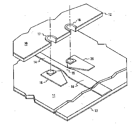
Referring now to Figure 1, a wideband stripline to microstrip
transition in accordance with the invention is shown. The
transition has a bandwidth extending from approximately DC to
20 gHz, with a low loss, and low reflectance through this
range. The transition is fabricated on conventional
substrate material requiring no external components and
requiring a minimum of space.
The inventive transition is designed to solve the
interconnection problem between stripline and microstrip, as
for example in circuit assemblies in which the active
circuitry is in microstrip and the passive circuitry is in
stripline. Thus, the Figure 1 arrangement, while having a
-- 5 --
"` ~29~6;~:~
rectangular outline depicting a single transition, will
normally find its place in a larger circuit assembly and be
replicated in large numbers when multiple signal paths
require multiple stripline-to-microstrip transitions. The
novel transition is formed using two conventional laminate
members 10 and 11 of unequal length assembled together to
form a stripline region where both members overlap (to the
left in Figure 1~ and a microstrip region where the longer,
lower member 11 is unlapped (to the right in Figure 1). The
upper member lO may be a commercially available microwave
laminate having a solid copper ground plane on the upper
surface (12) or a laminate having a copper layer on both
surfaces with the under surface layer being removed at the
time of assembly.
The lower laminate member 11 has metallization on both
surfaces. The original continuous copper layer on the upper
surface of 11 is sel~ctively etched or otherwise patterned to
provide the "finite" width central conductors 14-16 used in
both the stripline and in the microstrip regions of the
transition, while the ground plane 13 on the uhder surface is
unbroken. As shown, the lower laminate member and the
central conductors continue to the left into the stripline
domain and to the right into the microstrip domain of the
circuitry.
Returning now to the details of the transition, the ground
plane 12 bonded to the upper surface of the upper dielectric
layer lOI and the ground plane 13 bonded to the under surface
of the lower dielectric layer 11 become the two ground planes
of the stripline region.
The central conductor (14, 15, 16) disposed between the
dielectric layers 10 and 11 completes the stripline region of
the transition.
The finite central conductor (14, 15, 16) is shown extending
from the stripline region where it has a fixed finite width
- 6 -
~298~29
to the microstrip region where it also has a fixed finite
width. The stripline portion 14 of the central conductor has
a smaller width than the microstrip portion 16, the
dimensions being selected to achieve a 50 ohm characterisitc
impedance in each region. In addition, in the vicinity of
the inner edge of the upper laminate lO, conveniently defined
to be the "midpoint" of the transitional region, the
transitional portion 15 of the central conductor gradually
and continuously increases in width from the stripline
portion 4 to the microstrip portion 16.
For purposes of better understanding the invention, one might
observe that while there is dc electrical continuity between
the three regions, and while one might expect some portion of
any r.f. energy introduced into one port to be transferred to
a load connected to the other port, there is, without the
improvements yet to be described, a very substantial
discontinuity in the propagation of r.f. energy at the
midpoint of the transition.
One may visualize the reflection occasioned to the energy
entering from a source connected to the stripline region and
leaving via the microstrip region. The discontinuity between
a stripline connected directly to a microstrip may be
expected to reflect half of the energy back to the source.
This arises from the fact that, without more, the microstrip
region, into which the energy propagates, makes provision for
only the half of the stripline fields which propagate below
the central conductor, and no provision for the half of the
stripline fields which propagate above the central conductor.
One would expect half of the energy to be reflected back to
the source in the unimproved transition.
The novel transition, now to be described in detail, avoids
such reflections, and as will be seen, smoothly redistributes
the fields as one progresses from the stripline region to the
; microstrip region.
86Z9
The special means employed in the transition consist of a
pair of vertical conductors 17,18 flanking the conductor 15
near the midpoint of the transition, a pair of horizontal
conductors 19,20 also flanking the conductor portion 15 near
the midpoint of the transition, and an end sur~ace
configuration of the upper laminate and its metallization.
The vertical conductors (17,18) preferably are formed as
plated-through holes in the laminate members. The holes may
be drilled or otherwise made, and extend completely through
the laminates so as to permit electrical contact with the
ground planes 12 and 13. The hole walls are then plated with
a deposited metal which electrically connects the upper and
lower ground planes together. The serial connection of the
two vertical conductors with the two ground planes forms a
continuous grounded surface around the central conductor 15
at one section (i.e. B-B) in the transitional region.
The grounded surface, encircling the central conductor, then
permits the E field previously confined to regions above and
below the conductor to rearrange itself in a more even radial
distribution, with more lines of force having a lateral
orientation extending toward the vertical conductors on
either side. Since there is "conservation" of the field as
one proceeds along the transition, assuming reflection-free
transmission, an increase in lateral lines of force produces
an equal decrease in vertical lines of force, and the total
number remains the same.
The field redistribution produced by the two grounded
vertical conductors 17,18 is illustrated in Figure 2B. The
field redistribution does not all take place at one
coordinate but rather takes place gradually commencing near
the left edge of the conductors 17 and 18, and increasing
until one reaches a line drawn through their centers.
Through the region affected by the proximity of the vertical
conductors to the central conductor, the E fields are
distributed radially for a full 360 about the central
!36~
conductor 14 leading to the two ground planes and two
vertical conductors. In this region, the transmission mode
may be said to be coaxial in nature. Figure 2B illustrates
the field condition at the B-B cross~section.
The quasi-coaxial mode transitions to a double slot mode to
the right of the line of centers of the vertical conductors
as the two grounded horizontal conducting members 19, 20
flanking the central conductor 15 begin to redistribute the
field into the two slots in continuation of the transition to
the microstrip region~
The construction of the members 19 and 20 is illustrated in
Figure 1, which is an exploded view. The members 19 and 20
Are perforated, and in the assembled condition are connected
to the ground planes 12 and 13 by the conductive plating used
to form the vertical conductors 17 and 18. It will be noted
that the holes through which the vertical conductors 17, 18
extend are centered a small distance from the end surface or
termination of the upper laminate 10. If these holes were
left of circular section, as a possible alternative, they
would not be open through the end surface of laminate lO but
would be separated from it by a thin intervening wall of
dielectric material. However, the connection of the vertical
plating to the horizontal conductors 19 and 20 is enhanced by
removal of this intervening makerial, thus exposing the upper
surfaces of the horizontal conductors 19, 20 immediately
adjacent to the plat~d-through holes. This allows the
through-hole plating to bond to the top surfaces of the
horizontal conductors. The resulting non-circularity of the
holes and their plating in the upper laminate does not affect
the r.f. fields in the transition, because the r.f. fields
here are concentrated in the narrowed slots defined by the
horizontal conductors 19 and 20, leaving the more remotely
disposed plated surfaces in a relatively field-free region.
As illustrated in Figure 3, the members 19 and 20 extend to
the right along the transmission path from the left edge of
_ g _
lZ9E~6;~9
the vertical conductors 17 and 18 to the midpoint of the
transition region (the midpoint being defined by the right
edge of the upper laminate) and continue to the rightr to the
point or just beyond the point where the central conductor
has attained the full microstrip width.
The inner edges of the flanking horizontal members 19, 20 and
the outer edges of the central member create two horizontal
slots, which due to the grounded condition of members 19 and
20, allows the E field to concentrate between these edges as
a function of their mutual proximity. The flanking
horizontal members 19 and 20 con~erge inwardly on the central
conductor from the section B-B to the midpoint of the
transitional region at section D-D and diverge from the
midpoint toward the microstrip region until they terminate
short of the Section F-F. At the midpoint, the slots are of
minimum width, And effect the greatest horizontal
concentration of the E field.
Convergence of the horizontal flanking members 19 and 20 upon
the central conductor (14) from section B-B to the midpoint
(section D-D) produces a gradual increase in the horizontal
components of the field. At the section B-B, the horizontal
members have negligible effect on the fields since the
vertical conductors are equally close to the central
conductor. At the section C-C, the slot is now narrowed as
the horizontal members become closer to the central conductor
than the vertical conductors. At section C-~ the quasi
coaxial field as shown in Figure 2C, exhibits an increased
horizontal component.
The trend to concentration of the field in a horizontal plane
continues to the midpoint of ths transition where the slots
reach a minimum dimension. This occurs at section D-D and
the field is illustrated at Figure 2D. The mode at section
D-D may be termed a double slot mode, implying su~ficient
field concentration in the slots to allow the uppsr ground
plane (lO, 12) to be terminated without creating a
;
-- 10 -
,9~6; :9
discontinuity in propagation. This is true because most of
the lines of force now run horizontally, confined to the
slots, thus depleting the vertical fields to the upper or
lower ground planes. As a result, the removal of the upper
ground plane results in substantially no loss in the total
field, substantially no change in impedance and no creation
of reflections.
The slots begin to widen past the midpoint minimum at section
D-D and, as this occurs, the vertical fields to the lower
ground plane now increase leading to the transfer of all the
field to the region under the central conductor as in a
normal stripline. The field at section E-E, as illustrated
at Figure 2E, represents a partial conversion. At section E-
E, the mode of propagation is that of a coplanar waveguide.
As the slots widen past section E-E, the horizontal fields in
the slots continue to diminish. Once past the transition
region, as for instance at the section F-F, the horizontal
fields in the slots are extinguished, transferring all of the
field to the region between the central conductor (16) and
the bottom ground plane where a vertical field is formed as
illustrated in Figure 2F. The field distribution from this
point on is that of a microstrip transmission line.
Summarizing, the successive field distributions consist
initially of the stripline mode (Figure 2A) with vertical
fields above and below the central conductors, the quasi coax
mode (Figure 2B), the transitional mode (Figure 2C), leading
to the double slot line mode (Figure 2D) with horizontal
fields to either side of the central conductor. Next with
the termination of the upper ground plane, the horizontal
fields are converted via the coplanar waveguide mode of
Figure 2E, to the vertical field, immediately below the
central conductor.
The foregoing field redistributions can be made sufficiently
smoothly to retain a very nearly constant input impedance.
In the embodiment illustrated for 6 to 18 gHz operation, the
return loss at the input (S11) exceeds 17 db; the loss
~ 11 --
~LZ9~36;~9
forward (S21~ is less than 0.2 db, the loss in reverse (S12)
is less then 0.2 db, and the return loss at the output (S22)
exceeds 17 db.
These figures imply equal performance in either the stripline
to microstrip signal direction or in the microstrip to
stripline signal direction.
The dimensions of the exemplary line operating in the 6-18
gHz range are small. The hole dimensions for the vertical
conductors are 0.020" in diameter, and the thickness of the
substrate dielectric material, typically "Duroid"TM is
0.010". The conductive layers are 0.0011", and the width of
the central conductor in the stripline region is 0.0166" and
in the microstrip region 0.0307". The slots narrow to
0.0013" at the section D-D, and increase to 0.015" at the
edges of the members 19 and 20 toward the microstrip. At the
edges of the members 19 and 20 toward the stripline, the slot
distance is 0.020". The distance from the vertical members
to the central conductor is 0.020". The construction permits
a 50 ohm to 50 ohm characteristic impedance.
The construction is of substantial simplicity not re~uiring
intermediate transition materials. The vertical conducting
members 17, 18 in the transition may be plated-through holes
as earlier described, or they may be holes filled with a
conductive epoxy or metal post members electrically connected
to the ground planes and to the horizontal conducting members
19, 20. The inner wall dimensions of the vertical conductors
forming the quasicoaxial region and the configuration of the
horizontal conductors forming the slots may also be modified.
However, the illustrated contours represent an efficient
computer optimization, and provide a very simply built and
practical disposition. More parti¢ularly the central
conductor is of constant width throughout the stripline
section, is softly curved into the Pxpansion required as one
enters the microstrip mode and is of constant width
thereafter in the microstrip region. The five sided
- 12 -
~Z98~
horizontal conductors have straight inner edges and as
earlier noted, the vertical members are cylindrical and
easily drilled.
In a configuration for operation at a different impedance or
differing frequency, the dimensions will of course be
different. The transitions, also may be modified to reflect
either tighter or more relaxed tolerances.
While the transmission mode in Figure 2B is described as
quais-coax, for convenience the elctric field configuration
can also be modelled as for s suspended substrate line.
The terms "vertical" and "horizontal" hereinabove applied to
the elements of the transition are intended to describe the
position of the elements in relation to the planes of the
layers disposed in the stripline, microstrip, and
transitional regions, and not necessarily in relation to
earth-referenced planes. The assembly uses laminar layers,
conventional for printed circuit processing, all of which lie
in parallel planes. Accordingly, "vertical" has been
intended to mean perpendicular to these planes, and
"horizontal" has been intended to mean parallel to these
planes.