Note : Les descriptions sont présentées dans la langue officielle dans laquelle elles ont été soumises.
BIPOLAR TRANSISTOR WITH POLYSILICON STRINGER
BASE CONTACT
Backaround of the Invention
The invention pertains generally to the field
of bipolar transistor construction, and more
particulaely, to a bipolar transistor of extremely small
dimensions using a polysilicon stringer base contact.
The frequency response and switching speed of
bipolar transistors is related to the amount of
parasitic capacitance that results from the transistor
structure. In a bipolar transistor there is a junctio~-
capacitance associated with the emitter-base junction
and another junction capacitance associa~ed with the
base-collector junction. There are also other junction
capacitances such as the collector-substrate capacitance
which affect the operation of the transistor. Junction
capacitance is directly proportional to the area of ~he
junction. Therefore, the smaller the area of the
junction, the smaller will be the capacitance. Further,
in bipolar transistors there is a base resistance which
is made up of two components. The first~component i~
called the extrinsic base resistance, and is the
resistance of the path through the base region from ~he
center of the base contact to the edge of the emitter
region. The second component of the base resistance is
the resistance of the path through the base region from
the edge of the emi~ter to the center of the, emitter,
~ !3~ f
--2--
i.e., in the portion of the base region directly
underlying the emitter region.
It has long been known that if the size of the
base region can be reduced, and the width of the emitter
can be reduced, then beneficial effects will occur to
improve the performance of the transistor. One of these
effects is that the size of the emitter-base and
base-collector junctions will be reduced. This reduces
the parasitic capacitance affecting these junctions.
Further, if the size of the base region is reduced, the
extrinsic portion of the base resistance will also be
reduced by virtue of a shorter path length. Also, if
the size of the emitter can be reduced, the intrinsic
portion of the base resistance will also be reduced by
virtue of a shorter path length from the edge of the
emitter to the center of the emitter through the base
region. Since reduced path length reduces the total
resistance, the dimensional changes in the size of the -
base and emitter will result in lower parasitic
capacitance and lower parasitic resistance values. The
result will be a higher high frequency cutoff and a
lower switching speed.
Thus a need has arisen for a bipolar transistor
with base and emitter regions which are reduced in
size.
SummarY of the Invention
The invention fills the need for a bipolar
transistor having a reduced size base region and reduced
emitter region width thereby resulting in very high
performance. The invention, in one important aspect, is
a bipolar transistor structure having a silicide covered
polysilicon emitter contact stripe over an emitter
region in a 6ubstrate and silicide stringer base
.
.
1~&~21
contacts. The silicide base contact stringers are
formed on the sides of the emitter contact stripe normal
to the surface of the substrate, but are insulated
therefrom by silicon dioxide spacers in the form of
anisotropically etched stringers. The silicide base
contact stringers lead to a base contact window or post
type via located on a contact pad outside the perimeter
of the isolation island and leading to an overlying
metal layer with which the stringer base contacts may be
in contact. The base contact pad is silicide, and is
located outside the perimeter of the base region
isolation island. The silicide stringer base contacts
form extensions of the silicide of the base contact pad.
A silicide layer is formed on top of the
polysilicon stripe by depositing a layer of refractory
metal covering the entire layer of polysilicon covering
the entire surface of the die prior to the etching of
the polysilicon to define the emitter stripe. The die -
is then subjected to a heat pulse treatment in a known
fashion thereby causing the refractory metal to form
silicide everywhere it is in contact with polysilicon.
The emitter contact is a stripe of polysilicon
having a width equal to the minimum
photolithographically obtainable distance, D. In some
embodiments, the emitter contact stripe is more narrow
than the minimum distance D and is formed by overetching
the polysilicon stripe using a mask which has a width of
D. The silicide covering the polysilicon emitter
stripe is self aligned by virtue of its having been
formed prior to the etching of the polysilicon to form
the emitter stripe. The emitter stripe leads to a
emitter contact pad located outside the perimeter of the
base contact isolation island. Both the base and
emitter contact pads have dimensions which are large
~LZ~ 2~
--4--
enough to contain within their perimeters a contact
window or post type via which has a dimension equal to D
on all sides plus the area consumed by the alignment
margins on all sides of the window or via perimeter.
Such an alignment ~cushion~ area is necessary to prevent
loss of yield from alignment errors during fabrication.
In alternative embodiments, the polysilicon of the
emitter stripe can be extended to another place in the
circuit to make contact with another node in the
circuit, or it can extend over another isolation island
to form the emitter of another transistor which shares
an emitter with the original transistor from which the
polysilicon emitter stripe originated. The same thing
may be done with the silicide of the base contact pad.
These two layers therefore provide a "free~
interconnection layer under the first metal or
polysilicon interconnection layer.
The emitter contact stripe is separated from -
the silicide base contact stringer by an insulating
shoulder or spacer made of silicon dioxide. In other
embodiments, other insulating materials may be used
which are electrically and thermally compatible with the
electrical functioning of the transistor and its
structural integrity. This insulating shoulder is very
narrow by virtue of the process used to make it. The
process used to make this insulating shoulder involves
depositing a layer of CVD oxide over a thin layer of
thermally grown oxide such that the composite layer has
the desired thickness of the shoulder. This oxide layer
blankets the entire wafer area. Since the oxide layer
bulges at the location of the emitter stripe like a
blanket of snow would bulge if it fell on a two by four
piece of lumber lying on a flat surface, an anisotropic
etch step may be used advantageously to form,the oxide
21
--5--
shoulders. The anisotropic etch is continued long
enough to remove all the oxide over horizontal surfaces,
i.e., surfaces parallel to the surface of the substrate,
leaving only oxide adjacent to vertical surfaces, i.e.,
surfaces normal to the substrate surface. This causes
the formation of an oxide stringer along the edges of
the emitter stripe which completely insulate the surface
of the poly emitter stripe which is normal to the
surface of the substrate. These oxide stringers are
self aligned with the edges of the poly emitter stripe
at the intersection of the covered edges and the "top"
surface, i.e., the surface parallel to the surface of
the substrate. This insulating material stringer is the
insulating spacer or shoulder which will separate the
emitter stripe from the base contact stringers. This
insulating shoulder has the width of the original oxide
layer's deposit depth.
The silicide base contact stringer is formed i~
the same manner as was the insulating shoulder. After
the emitter polysilicon stripe is deposited and etched
and after the oxide insulating shoulder is formed, a
layer of silicide is formed by any conventional mannqr
over the entire wafer surface. This silicide is doped
to the proper polarity to form a base contact. The
silicide forms a blanket which covers the entire wafer
with bulges at the locations of all the emitter stripes
and oxide shoulders. An anisotropic plasma etch is then
used to remove all the silicide lying over surfaces
parallel to the surface of the substrate thereby leaving
silicide stringers formed on the surfaces normal to the
surface of the substrate. This forms a silicide base
contact over the base region isolation island adjacent
to the oxide shoulder and insulated from the emitter
contact stripe by the oxide shoulder.
~L2~921
The process for making the bipolar transistor
structure of the invention involves first manufacturing
an isolation island by any known method at every
location in the substrate where a transistor is to be
formed. In fact one isolation island should be formed
for each base-emitter area. Another isolation island is
formed for a collector contact. Any method of forming
these isolation islands can be utilized, but the
Fairchild Isoplaner ~ method is preferred. The
surface of the isolation island is preferably planarized
using known techniques to remove the "birds heads".
Preferably an N~ buried layer in a P- substrate is
formed at all isolation island locations where NPN
transistors are to be formed. A P- type epitaxial
silicon is formed over this buried layer to serve as the
base region.
Next a layer of polysilicon is deposited over
the entire wafer surface. Then a layer of silicide is -
formed over the entire polysilicon layer, and this
silicide is doped with both N and P type impurities to
N+ and P- concentrations respectively. Following
silicide formation, a layer of insulating material,
preferably silicon dioxide deposited by chemical vapor
deposition (hereafter CVD oxide) is deposited over the
entire silicide surface. The combined three layers are
then etched in a known manner to define the emitter
contact stripe and the emitter contact pad.
In some embodiments, the emitter contact poly
is overetched such that the photoresistant nitride
overhangs the edges of the poly. Preferably the
photoresist is developed such that the width of the
emitter contact stripe is the minimum
photolithographically obtainable distance, D. In
overetched embodiments then the emitter cont,act stripe
--7--
may be as narrow as one half the minimum
photolithographically obtainable distance, D.
Next the photoresist is dissolved, and a layer
of thermal oxide is grown so as to cover all exposed
silicon surfaces including the sides but not the top of
the polysilicon emitter stripe and the exposed portions
of the top surface of the P- epi.
To form the insulating shoulders, a layer of
CVD oxide is deposited over the entire wafer. The CVD
oxide is deposited to the approximate thickness desired
for the oxide shoulders to be formed less the thickness
of the thermal oxide already formed. Then an
anisotropic etch step is performed as described above to
form the oxide shoulder completely surrounding the
emitter contact stripe.
The base contact stringers and base contact pad
are next formed. The first step in this process is
forming a blanket layer of silicide, and doping it P+
for NPN transistors. Next an etch mask is formed over a
portion of the doped silicide overlying the end of the
emitter contact stripe at the opposite end from the
emitter contact pad. Finally, an anisotropic etch is
performed to form the silicide base contact stringers.
After forming the base contact stringer, it is
preferable to remove the portion of the stringer which
surrounds the emitter contact pad located outside the
isolation island for the base region since this allows
the emitter contact poly to be extended to other nodes
as an interconnection line. To do this, an emitter
stringer removal etch mask is formed by depositing,
exposing and developing photoresist such that it covers
the base region isolation island, the end of the emitter
contact stripe upon which the base contact pad will be
formed and all portions of the emitter con~a~t poly
- . : . . . .
stripe other than the emitter contact pad and a portion
of the emitter contact stripe which connects to the
emitter contact pad. A selective etch is then performed
to etch away all exposed silicide but not any exposed
CVD oxide or other insulation material thereby removing
the base contact stringers from around the perimeter of
the emitter contact pad.
Next, the emitter stringer removal etch mask is
removed. This leaves the base contact stringer and the
polysilicon emitter stripe and the emitter contact pad
exposed.
Next a heat drive-in step is performed to drive
impurities into the substrate from the silicide to form
the emitter contact, the emitter region and the base
contact region in the substrate. The entire structure
is heated to approximately 800 to 1000 degrees
centigrade for approximately 30 minutes. This causes
the N and P type impurities in the silicide overlying .-
the emitter contact stripe to outdiffuse into and
through the emitter contact stripe polysilicon. The P
type impurities outrun the N type impurities, and
diffuse into the substrate through the emitter contact
stripe to form a base region. The N impurities diffuse
into and through the emitter contact stripe and into the
substrate to form an emitter region. The P impurities
in the silicide base contact stringers diffuse into the
underlying substrate and form base contact regions of P+
concentration which join the P concentration base region
just formed.
This leaves the transistor structure complete
except for the formation of contacts to the emitter and
base contact pads from the external world.
Preferably contacts to the transistor are made
through post type vias through an overlying la~er of
.
.
silicon dioxide or other compatible insulating
material. However, in other embodiments standard
contact windows formed in overlying passivation layers
may also be used. In the preferred embodiment, the post
type vias are formed by depositing a thick layer of
photoresist over the entire structure. The photoresist
is then exposed to radiation everywhere except where the
post vias are to be formed. One via is located on the
emitter contact pad, and the other via is located on the
base stringer contact. The unexposed photoresist is
then dipped off to leave a hole in the thick photoresist
pattern at the location of each post. The metal of the
post is then deposited in a blanket over the entire
surface of the wafer. This metal goes down into the
holes in the photoresist, and also covers the top
surface of the photoresist. However, because of the
thickness of the photoresist, the step coverage at the
edges of the holes will be incomplete. The photoresist-
is then removed, and this will leave the posts standing
at the desired locations. Because the step coverage at
the edges of the holes in the photoresist is very bad,
removal of the photoresist will also remove all the
metal on top of the photoresist without effecting the
metal of the posts in the holes. This technique is
called the lift-off technique. However, other
techniques are known for forming posts, and any one of
these techniques will work for purposes of practicing
the invention.
AfteI forming the posts, a passivation layer of
insulating material is formed. This is done by
depositing a thick layer of CVD oxide to a height
greater than that of the posts. Then, this oxide i~
etched back until the tops of the posts are exposed.
This forms a planacized layer of oxide with,the tips of
~2~&G~l
64157-220
the posts exposed just above the planar surface. A metal
conductive layer can then be formed by conventional means to make
contact with the tops of the posts and thereby to make contact
with a transistor. Thereafter, another insulation layer may be
formed over the entire structure to passivate the circuit.
According to a broad aspect of the invention there is
provided a base and emitter structure for a bipolar transistor
comprising:
an island of monocrystalline silicon of a first conductivity
0 type electrically isolated from adjacent monocrystalline silicon
an emitter region of said first conductivity type within said
island;
a base region of a second conductivity type within said
island and forming a PN junction with said emitter region;
an emitter contact comprising a strip of polycrystalline
silicon of said first conductivity type in electrical contact with
said emitter region, the area of said emitter contact lying over
said island being smaller than the area of the smallest contact
window which can be made with the process used to make the base
emitter structure defined herein plus the area consumed by the
smallest nesting tolerance around all sides of said contact window
which can be used in said process, said emitter contact having a
top and sides;
a layer of insulating material over said emitter contact and
self aligned with the sides thereof;
s
, .
21
lOa 64~57-220
insulating spacers formed on at least said side surfaces of
said emitter contact over said island;
a conductive stringer formed over said island and alongside
at least one of said spacers and electrically isolated from said
strip by said spacers but ln electrical contact with said base
region wherein sald stringer has an area over said island which is
not large enough to encompass a contact window or post via plus
the area consumed by the nesting tolerance used in the process
used to make the transistor.
Accordinq to another broad aspect of the lnvention there
is provided a base and emitter structure for an integrated bipolar
transistor in an island comprising-
a base region of conductive silicon;
an emitter region of conductive silicon inside said base
region;
a conductor in electrical contact with said emitter region;
insulating spaceræ formed on predetermined sides of said
conductor;
conductive stringers in electrical contact with said base
region formed on predetermined sides of said insulating spacers
and insulated from said conductor by said spacers, said stringers
having a width approximately equal to the depth of the layer of
conductive material from which said stringers were formed by
anisotropic etching; and
means external to said island for making electrical contact
with said stringers and with said strip of polysilicon.
~Z~ a2~
lOb 64157-220
According to another broad aspect of the invention there
is provided a process for making a base and emitter contact
structure for a transistor comprising the steps of:
forming an isolated island of monocrystalline silicon;
forming a layer of polysilicon covered by a first layer of
metal disilicide;
doping the first metal disilicide layer with both P type and
N type impurities where the impurities are selected such that the
lower concentration impurity has a faster diffusion rate in terms
of distance travelled per unit time for given diffusion
conditions;
forming a layer of insulating material over said metal
disilicide;
etching said combined three layers into the shape of an
emitter contact strip which crosses said island and which has an
emitter contact pad located external to said island;
forming a second layer of insulating material over the etched
structure;
anisotropically etching the second insulating layer until all
the insulating material in planes parallel to the surface of said
island is removed;
forming a layer of second metal disilicide over the
structure;
doping said second metal disilicide layer with impurities of
the conductivity type which will exist in the base region of the
final transistor;
~i&`9;~
lOc 64157-220
masking a portion of said second metal disilicide layer which
is to be the base contact pad at a location outside said island;
anisotropically etching away all portions of said second
metal disilicide layer which lie in planes parallel to the surface
of said island except that portion under said mask; and
baking the resultant structure in an oven long enough and at
a temperature sufficient to allow the impurities in said first
metal disilicide layer to diffuse into said polysilicon and said
monocrystalline silicon sufficiently to form an emitter region of
the desired depth and a base region of the desired width which is
in electrical contact with said second metal disilicide layer.
According to another broad aspect of the invention there
is provided a contact structure comprising,
a semiconductor body having a major surface;
a first region of electrically conductive material disposed
on and in contact with the semiconductor body, the first region
having first sidewalls;
a first layer, of flrst thickness electrically insulating
material, disposed over the first region and on the first
sidewalls and extending to the major surface to thereby define
second sidewalls separated from the flrst sidewalls by the first
thickness; and
a second layer, of second thickness electrically conductive
material, disposed over at least the second sidewalls and
extending to the major surface to thereby define third sidewalls
separated from the second sidewalls by the second thickness.
~2~39Zl
lOd 64157-220
According to another broad aspect of the invention there
is provided a semiconductor structure comprising:
a semiconduc~or pocket having a major surface, the pocket
surrounded by insulating material;
an emitter disposed in the body ad~acent the major surface;
a base disposed beneath the emitter and extendlng to at least
a first side of the emitter;
a baæe contact disposed on the first side of the emitter and
extending between the major surface and the base;
an emi~ter contact region disposed on the major surface over
all of the emitter and extending onto the insulating material in a
first direction, the emltter contact having first sldewalls;
an insulating layer disposed over the first sidewalls and
extend~ng to the major surface, the insulating layer having a
first thickness to thereby define second sidewalls spaced apart
from the first sidewalls by the first thickness; and
a base electrode layer dlsposed over the second sldewalls and
extending to the major surface to the base contact, the base
electrode layer having a second thickness to thereby define third
sidewalls spaced apart from the second sidewalls by the second
thickness, the base electrode extending onto the insulating layer
in a second direction.
Brief Descri~tion of the Drawinas
Figure 1 is a cross-sectional view of the transistor
structure taken through the isolation island along the section
line 1-1' in Figure 2.
~2~&9Z~
lOe 64157-220
Figure 2 is a plan view of the finished transistor
structure.
Figure 3 is a plan view of two transistors of the
structure of the invention and having a shared emitter.
Figures 4A-4E are cross-sectional views of the
transistor of the invention taken along section line 4-4' in
Figure 2 through the emitter contact pad at various stages in the
process.
Figures 5A-5E are cross-sectional views of the
transistor taken along section line 5-5' in Figure 2 through the
isolation island of the transistor at various stages in the
process.
Figures 6A-6E are cross-sectional views of the
transistor taken along section line 6-6' in Figure 2 through the
base contact pad.
Figures 7A-7E are cross-sectional views of the
transistor of the invention taken along section line 7-7' in
Figure 2, whlch runs through the long dimension of the emitter
contact stripe, the base contact pad and the emitter contact pad.
Figure 8 is a plan view of the structure after the
emitter contact stripe has been formed.
- 1 1 -
Figure 9 is a plan view of the structure after
the insulating spacer has been formed.
Figure 10 is a plan view of the structure after
the base contact stringer has been formed.
5Figure 11 is a doping profile of the
base-emitter structure before the drive-in step.
Figure 12 is a doping profile after the
drive-in step.
Figure 13 is a cross-sectional view of a
conventional base-emitter structure.
Figure 1~ is a plan view of the base-emitter
contact structure of the invention illustrating it
typical dimensions and giving certain performance
related characteristics.
Detailed DescriPtionQ f the Preferred Embodiment
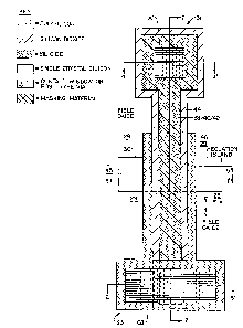
Referring to Figure 1, there is shown a
cross-sectional view through the isolation island of the
base and emitter contact structure for the transistor of
zo the invention. The section of Figure 1 is taken along
the section line 1-1' in Figure 2. Figure 2 is a top
view of the base and emitter contact structure for the
transistor of the invention showing the locations of the
contact pads for the base and emitter at positions
external to the perimeter of the isolation island. The
sectional view of Figure 1 shows only the base and
emitter contact structure and the base and emitter
regions in the substrate of the transistor of the
invention. The collector structure can be any
conventional structure, and those skilled in the art
will appreciate how any of these conventional collector
and collector contact structures can be connected to the
base and emitter structure of the invention.
~&~23
-12-
The invention will be described in terms of an
NPN transistor; however, those skilled in the art will
appreciate the changes which must be made in the doping
to make a PNP transistor. In Figure 1 an isolated
island of N type, epitaxially grown silicon 30
(hereafter epi) is defined by a field of oxide 29 of
which the edges which define the isolation island are
shown at 32 and 34. A buried layer 36 is shown under
the epi 30. Its presence is preferred, because it
lowers the series collector resistance. However, it may
be omitted without rendering the transistor inoperative,
and it will not be shown in subsequent drawings
describing the preferred process of the invention for
making the transistor of the invention.
An N+ doped polysilicon (hereafter poly)
emitter contact 38 is formed atop the epi 30. This poly
emitter contact has the shape shown in Figure 2, and
extends over the isolation island and out over the fiel~
oxide Z9 in the positive and negative y directions (in
accordance with the coordinate system shown in Figures 1
and 2; the origin is arbitrarily selected and may vary
from drawing to drawing) to the locations of an emitter
contact pad 31 and a base contact pad 33 located outside
the perimeter of the isolation island. The purpose of
this poly layer 38 is to provide a conductor to make
contact with an emitter region 39 in the epi layer 30.
This emitter region serve6 as a source of current
carriers which are injected into a base region 41 to
enable transistor action to occur. The manner in which
the emitter region 39 and the base regions 41 are formed
will be described in more detail below. In the
preferred embodiment, the emitter region of N+ doped epi
extends approximately 500 A below the sub~trate
surface 43.
. . . . .
~&921
-13-
In the preferred embodiment, the width of the
poly emitter contact 38 in the x direction is the
minimum achievable dimension, D, which can be obtained
using the process used to manufacture the transistor.
In optical photolithography in 1986, D is approximately
1 micron in many fabrication facilities. With further
improvements in photolithography such as use of X rays
as the radiation source, or through use of direct write
electron beam systems, Ds smaller than 1 micron are or
will become possible. Further, through use of
controlled overetch processing, D may be reduced to
approximately 0.6 microns.
It is preferable to make D as small às possible
so as to minimize the area of the base-emitter
junction. Minimizing the area of the base-emitter
junction by keeping D small minimizes the parasitic
capacitance of the base-emitter junction. This improves
the performance of the device by lowering the Miller -
effect input capacitance by decreasing the switching
speed of the device and by increasing the high frequency
cutoff of the transistor.
The poly emitter contact 38 is preferably 3000
A thick, but this dimension is not critical to the
invention. The poly emitter stripe 38 is completely
covered on its top surface with a self-aligned layer of
silicide 40. This layer of silicide 40 is self-aligned
with the edges of the poly emitter contact stripe 38
along both the x and y axes. That is, the poly contact
stripe 38 has edges which are parallel to the z axis and
which define the extents of the poly contact stripe 38
along the x and y axes. The edges of the silicide 40
define planes parallel to the y-z plane which are
coincident with the planes defined by the edges of the
poly contact stripe 38. The silicide layer 40 lowers
.
2~L
-14-
the sheet resistance of the poly contact stripe 38, and
its presence is preferred but not essential.
A layer of insulating material 42 is formed
atop the silicide layer 40 and the poly emitter contact
stripe 38. This insulating material is self-aligned
with the edges of the poly 38 and the edges of the
silicide 40. The term self-aligned, as it is used in
conjunction with the description of the structure of the
layer of insulating material 42, has the same meaning as
defined above for use of the term in conjunction with
the description of the silicide layer 40. The manner in
which the planes defined by the edges of the insulating
layer 42, the silicide layer 40, and the poly 38 become
coincident will become clear in the discussion below of
the preferred manner in which the structure shown in
Figure l is formed. In the preferred embodiment, the
insulating layer 42 is comprised of silicon dioxide
formed by chemical vapor deposition or low pressure --
chemical vapor deposition (hereafter CVD oxide). In the
preferred embodiment, the insulating layer 42 is
approximately 5000 A thick. The purpose of the
insulating layer 42 is to insulate the top of the
emitter contact 38 and its overlying silicide layer 40
(where used) such that a base contact pad may be
subsequently formed over one end of the emitter contact
without shorting the base and emitter contacts together.
The edges of the poly emitter contact 38 and
the silicide layer 40 (in embodiments in which this
layer 40 is used) must be insulated to prevent shorts to
the base contact stringers to be described below or to
other structures. To perform this function, an
insulating spacer 44 is formed around the edges of the
poly emitter contact 38, the silicide layer 40, and the
overlying insulatinq layer 42. This spacer;eXtends
.
3~
completely around the poly emitter contact 38 as is best
seen in Figure 2. The thickness is a matter of choice
as will be understood from the description given below
as to how the spacer is made. In the preferred
embodiment, the insulating spa/cerf44 is comprised of two
layers of oxide. The layer cloocd to the poly emitter
contact 38 is a thin layer of thermal oxide, and the
layer farthest from the poly emitter contact is CVD
oxide. Preferably, the spacer 4g is as narrow in the x
direction as possible without loss of its integrity as
an insulator so as to minimize the area of the substrate
and base regions which the spacer "shadows". By
minimizing the area of the cross-section of the spacer
in the x-y plane, the area of the base-collector
junction may be minimized. Those skilled in the art
will appreciate that smaller base-collector junction
areas lead to smaller parasitic junction capacitances
afflicting the junction which improves the performance
of the device in allowing faster switching speeds.
A base contact to the base area 41 is needed to
complete the base and emitter contact structure of the
invention. To further minimize the area of the
base-collector junction 43, the invention uses a
stringer base contact 46. In the preferred embodiment,
the stringer base contact 46 is formed of silicide which
is deposited or formed in any conventional manner. The
stringer base contact extends in the z direction to the
top of the insulating spacer 44, which itself extends to
the top of the insulating layer 42. This geometric
configuration of the insulating layer 42 is to prevent
any "crawl-out" of poly in the emitter contact 38 to
form silicide which might short the emitter contact 38
to the base contact stringer 46 and to prevent the
.
&~21
-16-
silicide layer 40 from accidentally shorting the emitter
contact 38 to the base contact 46.
The thickness of the stringer base contact 46
is very small, and can be controlled by controlling the
thicknes~ of the layer of silicide formed prior to the
etch step which forms the stringer, as will be seen from
the description of the process given below. This allows
the dimension of the base contact stringer along the x
axis to be kept at a minimum which is much less than D,
thereby allowing the designer to further minimize the
area of the base-collector junction.
To complete the base contact, a P+ doped region
48 in the epi layer 30 is formed directly below the base
contact stringer 46. The manner of formation of this
region 48 will be described further below. The P+ doped
region 48 extends laterally away in the positive and
negative x directions from the edges of the stringer
base contact 46, and joins and thereby makes electrical.
contact with the base region 41 to complete the base
contact structure. A final layer of CVD oxide (not
shown) is formed over the entire structure to passivate
it. This layer protects the base and emitter contacts
from shorts with overlying metal layers and seals the
structure from the ambient atmosphere.
Figure 2 shows a top view of the completed
emitter and base contact structure of the invention.
Identical reference numerals identify the same
structures in Figures 1 and 2. Note that the base
contact stringer 46 does not extend the full length of
the emitter contact stripe 38. Instead, the base
contact stringer 46 extends from the base contact pad
33, over the isolation island 30 and out over the field
oxide on the side of the isolation island opposite Prom
.
the base contact pad 33. However, the base,contact
.
~ 2~&~2:~
-17-
stringer 46 stops short of the emitter contact pad 31.
The reasons for ~his is twofold. First, the elimination
of the base contact stringer around the emitter contact
pad 31 prevents a base-emitter short in case of a
misalignment of a contact hole or post type via such as
post type via 50 on the emitter contact pad used to make
contact with the emitter contact structure. For
example, if the post via 50 were misaligned, such that
a portion of its area overlapped the perimeter of the
emitter contact pad 50, the metal of the post via 50
would contact both the emitter contact stripe and the
base contact stringer, thereby creating a base-emitter
short which would render the transistor inoperative.
This cannot happen when the stringer is removed from
around the emitter contact pad 31.
Another reason to remove the stringer from
around the emitter contact pad 31 is to simplify the
connection of the emitter of one transistor to the --
emitter of another transistor. It is very common in
integrated circuit structures to have two transistors
share a common emitter region and its associated emitter
contact structure.
Figure 3 shows such a situation. There, a
first transistor having isolation island 52 shares a
common emitter contact structure 54 with a second
transistor having an isolation island 56. A contact
window 58 or post type via serves as a connection point
for other nodes in the circuit or to the outside world.
The first transistor has a base contact pad 60 and a
contact window 62 to connect the base of transistor one
to other nodes in the circuit or to an external pin.
The second transistor has a base contact pad 64 for a
contact window 66 or post type via for connection of the
second transistor base to other nodes in the,circuit.
.
a21
-18-
Note how the absence of a base contact stringer 46
around the emitter contact stripe 54 simplifies the
interconnection of the two transistors since the poly of
the emitter contact for the first transistor may simply
be extended over the isolation island 56 of the second
transistor to form the emitter contact and emitter
region for the second transistor. If a base contact
stringer were present completely surrounding the emitter
contact stripe, two separate emitter contact stripes,
one for each island, would be required. The
interconnection of the two emitters would require two
emitter contact holes such as the contact hole 50 in
Figure 2 with a metal interconnection pattern etched in
a layer of metal overlying the CVD oxide passivation
layer to interconnect the two emitters. Such a
structure would consume more chip area because of the
area consumed by the extra contact hole and would tend
to cause more yield reducing defects caused by bad meta~
interconnection, e.g., gaps in the metal, or
misalignment errors.
However, in some embodiments, the base contact
stringer 46 may be left surrounding the emitter contact
stripe, and the base and emitter contact structure of
the invention will still be operative.
The extension of the emitter contact stripe
outside the perimeter of the isolation island 30 in
Figure 2 allows the isolation island to be smaller and
allows the base-emitter and base-collector junction
areas to be smaller. The reason for this is that if a
contact window to the emitter must be formed within the
perimeter of the isolation island, the emitter stripe 38
must be large enough to encompass a contact window plu6
surrounding alignment cushions.
~ ~G ~
These alignment cushions are sometimes referred
to as "nesting tolerance~ and refers to a design rule
tolerance used where a feature on a particular level of
an integrated circuit must be nested within a feature on
another level of an integrated circuit. The nesting
tolerance is necessary because of several uncertainties
in the manufacturing process. These include the
uncertainty of the exact location of the edge of the
feature on the first level and the uncertainty of the
exact location of the edge of the feature on the second
level and the uncertainty of the overlay alignment
exactness. The size of mask features can vary from chip
to chip on the mask because of improper exposure, and
other factors. An absolute size variation of + or - 0.2
micrometers across a 125 millimeter square mask is not
uncommon. When these variable size mask features are
lithogra~hically transferred to a wafer, more deviation
from the original layout occurs. The resist image can -
vary from the mask image because of variations in any or
all of the lithographic processing variables, such as
resist thickness, baking temperature, exposuee, and
development conditions. The etching process which
transfers the resist image into the polysilicon or other
material can also vary the etched image size from wafer
z~ to wafer and from day to day because of variations in
the isotropy of the etch process. An absolute variation
of the final etched image of + or - 0.4 micrometers over
a year of production is easily possible.
An emitter which required an area over the
isolation island which was large enough to nest a
contact window plus the area consumed by the nesting
tolerance would be substantially larger in area than the
- emitter stripe 38 of the structure of Figure 2. This is
because the smallest contact window which can be made
~ 2~&~,2~
-20-
has a dimension D on each side. To allow for alignment
errors, an alignment error cushion must be left on all
sides of the contact window. The resultant minimum
emitter contact dimension on one side is D plus the
alignment cushion, C. The result is a minimum emitter
contact area of (D + C) = D + 2DC + C . This
results in a larger emitter- base junction area because
the emitter region 39 in Figure 1 is formed by
outdiffusion of impurities from the emitter contact
poly. Thus the emitter-base junction area is defined by
the area of the emitter contact. By putting the emitter
contact window outside the perimeter of the isolation
island, the emitter contact 38 may be made with a
dimension of one D or less on a side, thereby minimizing
the emitter-base junction area and the parasitic
capacitances which exist at this junction.
The same logic as given above for the
minimization of the emitter-base junction area applies -
equally to the minimization of the base contact size and
the base-collector junction area. That is, if the base
contact over the isolation island had to be large enough
to encompass a base contact window, the base contact
area over the i~olation island would be much larger than
the area under the base contact stringer 46 of the
invention. Since the base-collector junction area
generally encompas~es the total area "shadowed" by the
emitter contact, i.e., over which the emitter contact
lies, plus the area shadowed by the base contact plus
any insulating spacers between these two contacts, it is
of paramount importance to minimize all these areas to
minimize the base-collector junction area and the
associated junction para~itic capacitance. The total
shadowed area is minimized by use of a base contact
stringer 46 and an insulating spacer 44 which is formed
-21-
in the same manner. These stringers can be made much
smaller than the minimum line width D which can be
obtained with the photolithography process. By
extending the base contact stringer 46 to the location
of the base contact pad 33, and by expanding the base
contact stringer to form a base contact pad which is
large enough to encompass a contact window such as the
window 68 plus an alignment cushion, a smaller
base-collector junction area can be obtained with no
loss in yield. This can be done without the
complications of trying to make a very small contact
window and align it over a very small base contact pad
located within the perimeter isolation island. With the
structure of the invention, ample sized contact windows
lS may be easily aligned over contact pads which are sized
to have adequate alignment error cushions to make
alignment easy.
Process Seguence
There follows a description of a preferred
process for making the structure of Figures 1 and 2.
The proces6 will be described with the aid of a series
of sectional drawings taken as a time sequence through
various sections in the final structure shown in Figure
2.' A series of sectional views labeled Figure 4A, 4B .
. . will detail the structure at the section line 4-4'
in Figure 2 through the emitter contact a various stages
in the process. A series of sectional views labeled
Figure 5A, SB . . . will detail the structure at the
section l-ine 5-5' in Figure-2 through the isolation
-' island at vari,ous stages in the- proce6s. ,Fi'gure 1 shows
the final structure minus the final layer of insulating
material for passivation. A series of sections labeled
Figure 6A, 68 . . . will detail the structure at the
-22-
section line 6-6' in Figure 2 through the base contact
at various stages in the process. A series of sections
labeled Figure 7A, 7B . . . will detail the structure at
the section line 7-7~ in Figure 2 longitudinally through
the emitter contact stripe along the y axis at various
stages in the process.
Fabrication of the transistor starts with the
conventional growth of a layer of epitaxial silicon 30
followed by the conventional formation of an isolated
regions or isolation island of epitaxial silicon
surrounded on all sides by field oxide 29 which extend
completely through the epitaxial layer 30. Any of the
many ways of forming isolated regions of epi will
suffice, but the Fairchild Isoplanar~ method is
preferred. This method is well known in the industry,
and needs no further discussion here. It is also
preferred to form P~ channel stop implants such as those
shown at 70 in Figure ~ under the field oxide and
completeiy surrounding the isolation island 30. The
purpose of these channel stop implants, as is well
known, is to prevent the formation of conductive
channels in parasitic MOS transistors under the field
oxide, thereby preventing true electrical isolation of
the island 30 from other nearby islands. Such channel
stops are not critical to the invention and may be
omitted of these parasitic MOS transistors are not
formed or otherwise are not a problem. The channel
stops 70 will not be shown on subsequent drawings for
simplicity.
~igures 4A through 7A show the transistor
structbre at an early stage in the processing after the
isolation island 30 has been formed and a layer of
intrinsic poly has been deposited after a layer of
silicide 74 has been formed on top of the poly and
. . . . . .
.
-
~ ~&~
-23-
during an implant of impurities into the silicide.
After formation of the isolation island, a layer 72 of
undoped polysilicon 72 is deposited as shown in Figures
4A through 7A. Deposition of the layer of poly 72 is by
any known method such as chemical vapor deposition.
After the poly layer 72 is deposited, a layer
of silicide 74 is formed over the poly layer 72. The
silicide layer 74 may be formed in any conventional
manner. Two known ways of forming silicide are, first,
by depositing the silicide directly using a reaction
chamber and second, by aepositing a layer of
refractory metal over a layer of the polysilicon and
then heat treating the metal layer with a short heat
pulse to cause the polysilicon and metal to react and
form a silicide. The manner in which the silicide layer
74 is formed is not critical to the invention.
Following formation of the silicide layer 74,
an implant step or steps is performed. The purpose of -
this implant is to dope the silicide layer 74 with both
P type and N type impurities. These impurities will
later be driven out of the silicide by a heat step and
will diffuse into the poly layer 72 to dope it N+ and
into the epi 30 under the poly emitter contact stripe 38
to form the N+ emitter region 39 and the P- base regions
41 in Figure 1. During the implant shown in Figures
4A-7A, the silicide 74 is doped N+ to a concentration of
approximately 102 atoms per cubic centimeter and is
also doped P- to a concentration of approximately 10
atoms per cubic centimeter. Accordingly, the energy
level of the implant of these two impurities and the
dosage level should be such that the silicide layer 74
reaches the above concentration levels.
Following the implant of the silicide layer, a
layer of CVD oxide (not shown in Figures 4A ~hrough 7A),
.. . . .
' ' ' - '.
~f~c~ v ~ i
-24-
which is approximately 5000 A thick, is deposited over
the entire wafer. This CVD oxide will be etched along
with the silicide layer 74 and the poly layer 72 to form
the oxide layer 42 in Figure 1. Other compatible
insulating materials may be substituted for the CVD
oxide layer 42 in some embodiments. After this CVD
oxide layer is deposited, photoresist is deposited,
exposed to a radiation source through a mask and
developed to form an etch mask in the shape shown in
Pigure 8. The outline of this etch mask is shown at 76
in Figure 8. Once the etch mask is formed, the poly
layer 72, the silicide layer 74, and the CVD oxide layer
are etched, preferably by an anisotropic plasma etch, to
form the emitter contact stripe and the emitter contact
pad 31. The emitter contact stripe is comprised of the
poly stripe 38 in Figure 1 with the self-aligned
silicide layer 40 formed thereover and the self-aligned
CVD oxide layer 42 formed over the silicide layer. The.
silicide layer 40 and CVD oxide layer 42 are both
self-aligned with their edges coincident with the edges
of the poly 38 because of this single etch step, i.e.,
all three layers are etched simultaneously using the
same etch mask.
In some embodiments where it is desired to make
an emitter contact stripe which is more narrow along the
x axis than the minimum dimension D, an isotropic etch
with a controlled lateral etch can be used for the etch
step symbolized by Figure 8. In such embodiments, the
width of the etch mask 76 in the x axis over the
isolation island is set at one D. After the photoresist
is developed, an isotropic wet etch or an isotropic
plasma etch is used to define the emitter contact
stripe. The etch should have a known, well-controlled
etch rate in the x and y directions relative,to its etch
~Z~2:~
-25-
rate in the z direction. If this is the case, the final
width of the emitter contact stripe in the x direction
for a given thickness of the poly 38, the silicide 40
and the CVD oxide 78 can be accurately predicted if the
thickness of the combined poly/silicide oxide emitter
contact stripe is known and the etch time is known. In
such embodiments, emitter widths of 0.6 microns may be
achieved. Of course the masked area defining the
emitter contact pad 31 should be adjusted in such
embodiments to leave an adequately sized pad 31 after
the overetching occurs.
In alternative embodiments where the silicide
layer 40 is not used, the steps to this point in the
process are identical except that the impurity ions are
~, 15 implanted into the poly layer ~ instead of into the
silicide layer 74.
The next steps in the process are for the
purpose of forming the insulating spacer 44 around the -
emitter contact stripe. Referring to Figures 4B through
7B the structure of the invention is shown during the
anisotropic etch which forms the spacer 4~. One or more
intermediate steps precede this anisotropic etch step.
Because the spacer 44 insulates the emitter contact
stripe from the base contact stringer, it is important
that the electrical integrity of this insulating spacer
44 be as high as possible. Although in some embodiments
a layer of CVD oxide 78 may be used alone, in the
preferred embodiment, a layer of thermal oxide 80 is
grown over the exposed surfaces of the silicide layer 40
and the poly layer 38 and any exposed epi in the
isolation island 30 before the CVD oxide layer 78 is
deposited. CVD oxide is known to have more pinhole type
defects in it than does thermally grown silicon dioxide
. . . .
(hereafter thermal oxide). By first growing,a layer of
-26-
thermal oxide 80 over all exposed edges of the emitter
contact stripe which can be oxidized and then depositing
the CVD oxide, the electrical integrity of the spacer 44
can be improved. However, the use of the thermal oxide
layer 80 is not absolutely essential, and it can be
eliminated in some embodiments. Indeed, the use of
oxide as the insulating spacer 44 is not essential, and
other compatible insulators may be used in some
embodiments. In fact, although preferred, the use of
oxide as the insulation spacer 44 is not essential.
Other insulating materials which are thermally,
electrically, and mechanically compatible with the
polysilicide/CVD oxide sandwich making up the emitter
contact stripe will also work. The thickness of the CVD
oxide layer 78 should be the desired thickness of the
spacer 44.
After the thermal oxide 80 and CVD oxide 78 are
formed, the spacer 44 is formed by an anisotropic etch -
step symbolized by the arrows in Figures 4B throuqh 7B.-
This anisotropic etch step is generally a plasma etch,and the type of etchant ions and etching conditions to
achieve anisotropy are well known to those skilled in
the art. The desired end result is that all the CVD and
thermal oxide from the layers 78 and 80 respectively
79
llying in the x-y plane is etched off leaving intact
only the CVD and thermal oxide from the layers 78 and 80
lying in the x-z and y-z planes. The etch time must be
set such that this end result is achieved. If the etch
time is longer than the time needed to remove the CVD
oxide and thermal oxide in the x-y plane, some of the
oxide in ~he layer 42 will be removed. This will not be
harmful as long as an excessive amount is not removed.
- Figure 9 shows the emitter contact stripe after
the spacer 44 has been formed. Note how the,spacer 44
. ' ' - . . , ' ' . , .
.
-27-
extends all the way around the emitter contact stripe.
The height of the spacer 44 in the z direction will be
even with the top surface of the CVD oxide layer 42,
i.e., the surface in the x-y plane of the CVD oxide 42
farthest from the surface 43 of the isolation island in
Figure 1. The width of the spacer 44 in the x and y
directions is approximately 3000 A in the preferred
embodiment.
Figures 4C - 7C illustrate the stage in the
processing in the various sections in the device after
the insulating spacers 44 have been formed and during
the step of implantation of a layer of silicide which
has been deposited over the entire wafer. The layer of
silicide 82 may be formed in any conventional manner
lS which allow formation of silicide over oxide.
Preferably, it is formed by directly depositing the
silicide in a reaction chamber in a process which is
well known in the art. The process used to deposit the.
silicide must be one where silicide can be successfully
formed over oxide since it is imperative that the oxide
spacers 44 be completely covered with silicide. This is
necessary so that the stringers 46 of the base contact
can be formed.
Since the silicide layer 82 is to become the
base contact, it must be doped P+ for an NPN
transistor. The silicide layer 82 is very similar to
polysilicon in that it can be doped with impurities and
is conductive. Accordingly, the silicide layer 82 is
implanted with P type impurities as shown in Figures 4C
through 7C. The implant energy and dosage should be
such that the resultant silicide is P type in
conductivity and has a concentration of approximately
102 atoms/cm3.
?~
--28--
The next step is to form the silicide base
contact stringers 46 by means of an anisotropic etch.
ThiG anisotropic etch is symbolized by the second set of
arrows in the 2 direction in Figures 4C through 7C. The
particular manner in which this anisotropic etch is
accomplished is well known to those skilled in the art.
The purpose of this etch is to remove all the silicide
of the layer 82 which is in the x-y plane while leaving
the silicide which is in the z-y plane. Accordingly, an
etchant and etch conditions should be used such that the
etch is preferential along the z direction while very
little etching occurs in the y and x directions. The
etch time must be such that all the silicide of the
layer 82 which lies in the x-y plane is removed and the
top of the oxide layer 42 is reached. However before
this anisotropic etch is performed, a base contact pad
etch protect mask must be formed over the silicide layer
82 at the location where the base contact pad is to be -
formed. The location of the base contact pad is shown
at 33 in Figure 2.
Referring to Figure 7C, there is shown the
relative location of the base contact pad etch protect
mask 84. The purpose of this mask 84 is to protect the
doped silicide layer 82 during the anisotropic etch step
such that the silicide of the layer 82 lying underneath
the mask 84 is not etched away during the anisotropic
etch step to form the base contact stringers 46.
Accordingly, this mask 84 must be formed after the P
type implant step used to dope the silicide layer 82 to
P+ conductivity and before the anisotropic etch step
used to form the base contact stringers 46.
The mask 84 is formed in conventional manner
using photoresist. It should have the shape of the base
contact pad 33 in Figure 2, and it should shadow a
:, ' ' ' '
-29-
sufficient area of the silicide layer 82 that a contact
window or post type via such as the window 68 in Figure
2 can be easily formed therein taking into account the
alignment tolerances which can be consistently met in
the fabrication facility where the devices are
fabricated.
Figures 4D through 7D show the state of the
device after the anisotropic etch step to form the base
contact stringers 46. Note that Figure 6D shows that
the base contact pad 33 is formed over the emitter
contact stripe ~8 and is completely insulated therefrom
by the oxide layer 42 and the oxide spacers 44 including
the thermal oxide layer 80 in the preferred
embodiment. Figure lO shows the resultant structure in
plan view after the anisotropic etch step to form the
base contact stringers 46 and after the base contact pad
etch protect mask 84 is removed. Note in Figure lO that
the base contact stringer 46 extends completely around -
the emitter contact stripe 38.
As noted above, the base contact stringer 46 is
preferably removed from around the emitter contact pad
- 31. To accomplish this stringer removal, a stringer
removal etch mask 86 having the outline shown in phantom
in Figure lO is formed over each transistor on the
wafer. This stringer removal mask is formed by
developing photoresist in the pattern shown in phantom
so as to leave a protective layer of cross linked
photore6ist covering all the structure within the
phantom line 86 in Figure lO. The structure is then
exposed to a selective etch which attacks silicide but
which does not attack oxide. Such etches are well
known. This selective etch removes all the exposed
stringer 46 which is not covered by the etch mask 86.
This leaves the structure as shown in Figure, 2 with the
.
--30--
base contact stringers 46 extending around the base
contact pad 33, across the isolation island 30 and along
the emitter contact stripe part of the way toward the
emitter contact pad 31. However, the base contact
stringers 46 stop at the perimeter of the etch protect
mask 86 in Figure 10. As noted earlier, removal of the
stringer 46 is not necessary to make an operative
transistor. However, such removal does make it easier
to fabricate a multiple transistor structure with shared
emitters such as that shown in Figure 3.
After removal of the stringers 46 from around
the emitter contact pad 31, it is necessary to perform a
heat step to drive the impurities in the silicide layer
40 out of the silicide and into the emitter contact
lS stripe poly 38 and into the epitaxially grown silicon 30
to form the emitter region (39 in Figure 1) and the base
region (41 in Figure 1). During this heat step,
impurities are also driven out of the P+ doped base -
contact stringers and in~o the epi 30 to form better
base contacts.
Figures 4E through 7E indicate the final
configuration of the base and emitter contact structure
for the transistor of the invention after the heat drive
in step but before the final passivation layer is formed
and before any contact windows or po6t type vias are
formed. With particular reference to Figure 4E, it will
be noted that the base contact stringer6 46 are absent
from the positions around the perimeter of the emitter
contact pad 31. With particular reference to Figure 5E,
the effects of the heat 6tep can be ob6erved. In the
preferred embodiment, the heat step is performed in an
oven heated to a temperature of 900oC for 1/2 hour. As
noted earlier, the silicide layer 40 had been doped N+
with arsenic and P- with boron when thi~ silicide layer
~z~
40 was first formed. Similarly, the base contact
stringers 46 were doped P+ with boron when the layer of
silicide from which they were formed was first
deposited. During the heat step, the N and P type
impurities from the silicide layer 40 diffuse downward
into the polysilicon of the emitter contact stripe 38
and into the epitaxial silicon 30 in the isolation
island. The P type impurities also diffuse downward,
and, since these P type impurities move faster than the
N type impurities under the same diffusion conditions,
they overtake the N type impurities. When the-P type
- impurities outrun the N type impurities as they diffuse
through the emitter contact stripe poly 38 and the
epitaxial silicon 30 in the isolation island, they form
the emitter and base region6. The final result is an
emitter region 39 which i8 formed to a shallow depth in
the epitaxial silicon 30 and a narrow base region 41
which has a base width in the z direction which is equal-
to the difference in diffusion speed6 times the duration
of the diffusion. The diffusion time should therefore
be adjusted such that the desired base width is
obtained. Further the diffu6ion time should be long
enough that the N type impurities have time enough to
reach and make a shallow penetration of the epitaxial
silicon 30. If the N type impurities have time to reach
and penetrate the epi layer 30, then the P type
impurities will also reach and penetrate the epi 30 some
small distance further than the N type impurities
penetrated.
Figure 11 illustrates the impurity
concentration profile in atoms/cc plotted versus
depth in the structure before the drive-in step. Depth
line repeesents the top (most positive z) of the oxide
layer 42. No impurities are present in the oxide layer
-32-
42. Depth line B represents the depth of the interface
between the oxide layer 42 and the silicide layer 40.
The boron and arsenic doping concentration curves in the
silicide region between depth lines B and C represent
the effects of the separate P type and N type implants
in the silicide layer 40 after the layer was formed and
before the emitter contact stripe was formed. Of course
this doping may be accomelished in other ways, and any
way which is capable of doping the silicide layer 40 to
N~ concentration (10 ) and P- (10 ) will suffice
for purposes of practicing the invention. The depth
line C represents the interface between the silicide
layer 40 and the poly 38 of the emitter contact stripe.
The poly 38 extends between the depth lines C and D. No
impurities are present in the poly before the drive-in.
The depth line D indicates the surface of the epi region
30 which is doped N- at the 10 level.
Figure 12 is the doping profile after the
drive-in. The doping concentration in the silicide 40
after the drive-in is somewhere less than 102 N type
and somewhere less than 1018 P type. The doping level
in the poly 38 is 10 N type and 10 P type.
Starting at the surface of the epi layer 30, depth line
D, the doping concentration is N type for a penetration
of about 500 A to form the emitter region 39, and then
changes to P- type for about S00 A to form the base
region 41. The doping reverts to N- at about 1000 A
from the surface. The base-emitter junction is thus
about 500 A deep, and the base-collector junction is
about 1000 A from the surface.
Referring again to Figure 5E, the drive-in step
also causes P+ base contact regions 48 to be formed
underneath the base contact stringers 46 in the
epitaxial silicon 30. These regions 48 are caused by
~&~2~
the out diffusion of the P type impurities from the base
contact stringers 46 into the epitaxial silicon 30. The
diffusion time selected for the drive-in should be ~uch
that the P+ base contact regions 48 laterally diffuse
far enough to join the outward diffusion in the positive
and negative x directions of the P type impurities from
the silicide layer 40. This provides a good contact
structure for the base region of the transistor.
Figure 6E i8 the same as the Figure 6D in that
the structure of the base contact pad 33 i8 unchanged by
the heat step and unchanged by the selective silicide
etch to remove the base contact stringer from around the
emitter contact pad.
The final steps in completing the transistor
lS structure are to deposit a layer of planarized
- insulating material over the entire ~tructure and to
etch contact holes or otherwise form post type vias to
make contact with any base or emitter contact pads which
are to be connected to an overlying metal layer.
Alternatively, as shown in Figure 3, the emitter contact
poly stripe 38 can be extended over the field oxide to
the position of another transistor and formed over the
isolation island of that transistor 80 as to form a
shared emitter contact.
Figure 7E shows a final view of the structure
after the heat step, and includes the final passivation
layer of insulating material 88 through which contact
holes or post type vias such as those shown at S0 and 68
are formed. It will be noted that the base-emitter
junction 45 and the base-collector junction 43 in Figure
7E both terminate on the field oxide 29 thereby
providing low junction leakage cha~acteristics.
The advantages of the invention are manifest.
To best illustrate them requires a compariso,n with a
.
.
~&~
-34-
conventional base-emitter structure. A prior art
base-emitter structure is shown in Figure 13. In Figure
13, the emitter junction is shown very conservatively at
one micron in width. In reality, this would probably be
unachievable since the minimum contact window dimension
i6 generally one micron in today's process technology in
most fabrication facilities. The base-collector
junction is 3+1+3 microns or 7 microns wide. If the
depth into the page of the isolation island is one
micron, then the total area of the base-collector
junction is 7 microns2. There is associated with the
base contact structure of the device of Figure 13 a base
resistance which i8 comprised of the resistance from the
base contact window to the center of the base region
under the center of the emitter region. Traditionally,
this is divided into two components: rbe, or extrinsic
base resistance comprising the resistance of the path
through the lightly doped base epi from the center of
the base contact to the edge of the base-emitter
junction; and rbi, or intrinsic base resistance
comprising the resistance of the path through the base
epi from the edge of the emitter to the center of the
base region under the center of the emitter. Because of
the light base doping and the thinness of the base
region under the emitter region, the extrinsic base
resi6tance is typically 1000 ohms and the intrin6ic base
resi6tance is typically 10,000 ohms in the structure of
Figure 13.
The high frequency cutoff and switching speed
for bipolar tran6istor6 is generally proportional to the
time constant of the RC circuit comprised of the base
resistance and the junction capacitance of the
collector-base junction. If the extrinsic and intrinsic
base resistance goes up, the time constant gets greater,
2~
-35-
and the frequency response gets worse and the switching
speed becomes greater in the sense that fewer
transitions from the off state to the on state and back
again can be made per unit of time. The same result
occurs if the junction capacitance of the collector-base
junction becomes greater which generally happens if the
area of the collector-base junction becomes greater.
The factors that affect the base resistance are
the base doping, the path length, and the base width.
Shorter path lengths give less base resistance. The
path lengths are related to the size of the junctions.
The collector-base junction capacitance is
comprised of-two components: the space charge or
junction capacitance and the transition or diffusion
capacitance. The space charge capacitance is larger for
larger junction areas. The diffusion capacitance
increases with increasing current. The diffusion
capacitance is thus a factor only when the transistor is
in saturation and the collector-base junction is forward
biased. Since current is equal to current density at
the junction times the junction area, the diffusion
capacitance will be less for a smaller junction.
Smaller junction capacitance, like smaller base
resistance leads to faster switching speeds and bet~er
frequency response.
Figure 14 illustrates the typical dimensions of
the base-emitter contact structure of the invention.
Note that the emitter i8 shown as 0.5 microns in width
which is achievable if the overetching process-step to
define the emitter contact stripe is used or if a
lithography or other type of process which is capable of
achieving submicron line widths is used to manufact~re
the transistor. The total width of the active area in
the x direction i6 only 2 microns. This nar,row width
21
for the active area exists because the insulating
spacers 44 and the base contact stringers 46 can be made
very narrow by virtue of the process with which they are
made. In the preferred embodiment, the insulating
spacer 44 and the base contact stringer 46 are only 3000
A wide in the x direction. If the isolation island
dimension in the y direction is only one micron, then
the total active area and the total area of the
base-collector junction is 2 micron . This yields a
very low collector-base capacitance of 0.4 femptofarad.
The emitter-base junction is only 0.5 microns2 which
yields a typical base-emitter junction capacitance of
0.3 femptofarad. In contrast with the junction areas of
the conven~ional structure of Figure 13, it will be
appreciated by those skilled in the art that the
invention enjoys a considerable advantage in terms of
chip are consumed by each transistor active area and a
considerable advantage in switching speed and frequency-
response.
Although the invention has been described in
terms of the preferred embodiment, those skilled in the
art will appreciate that numerous modifications to the
structure or process are possible without departing from
the true spirit and scope of the invention. All such
modifications are intended to be included within the
scope of the claims appended hereto.
.