Sélection de la langue

Search

Sommaire du brevet 1299719 

Énoncé de désistement de responsabilité concernant l'information provenant de tiers

Une partie des informations de ce site Web a été fournie par des sources externes. Le gouvernement du Canada n'assume aucune responsabilité concernant la précision, l'actualité ou la fiabilité des informations fournies par les sources externes. Les utilisateurs qui désirent employer cette information devraient consulter directement la source des informations. Le contenu fourni par les sources externes n'est pas assujetti aux exigences sur les langues officielles, la protection des renseignements personnels et l'accessibilité.

Disponibilité de l'Abrégé et des Revendications

L'apparition de différences dans le texte et l'image des Revendications et de l'Abrégé dépend du moment auquel le document est publié. Les textes des Revendications et de l'Abrégé sont affichés :

  • lorsque la demande peut être examinée par le public;
  • lorsque le brevet est émis (délivrance).
(12) Brevet: (11) CA 1299719
(21) Numéro de la demande: 1299719
(54) Titre français: SOURCE INFRAROUGE A SUPER-RESEAU SEMICONDUCTEUR
(54) Titre anglais: SEMICONDUCTOR SUPERLATTICE INFRARED SOURCE
Statut: Périmé et au-delà du délai pour l’annulation
Données bibliographiques
(51) Classification internationale des brevets (CIB):
  • H01L 33/06 (2010.01)
  • H01S 05/34 (2006.01)
(72) Inventeurs :
  • LIU, HUI CHUN (Canada)
(73) Titulaires :
  • NATIONAL RESEARCH COUNCIL OF CANADA
  • HUI CHUN LIU
(71) Demandeurs :
  • NATIONAL RESEARCH COUNCIL OF CANADA (Canada)
  • HUI CHUN LIU (Canada)
(74) Agent: R. JOHN HALEYHALEY, R. JOHN
(74) Co-agent:
(45) Délivré: 1992-04-28
(22) Date de dépôt: 1989-01-13
Licence disponible: S.O.
Cédé au domaine public: S.O.
(25) Langue des documents déposés: Anglais

Traité de coopération en matière de brevets (PCT): Non

(30) Données de priorité de la demande: S.O.

Abrégés

Abrégé anglais


TITLE
SEMICONDUCTOR SUPERLATTICE INFRARED SOURCE
INVENTORS
HUI CHUN LIU
ABSTRACT
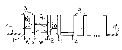
An infrared emitting semiconductor device having
a layer-shaped infrared emitting region with a superlattice
structure. The superlattice structure consists of thin alternating
narrow and wide wells separated by thin barriers. The narrow
well has one quasibound state E'0 while the wide well has two
states E0 and E1 with E0' being located between E0 and E1.
Under proper bias, an electron in state E0 can resonately tunnel
out of the well through the quasibound state E'0 to the first
excited state E1 of the next wide well. This electron can
then relax to the ground state E0 where it can resonately tunnel
to the next wide well and repeat the process. Infrared radiation
with its photon energy equal to E1-E0 is emitted as the electrons
relax from E1 to E0 in the wide wells.

Revendications

Note : Les revendications sont présentées dans la langue officielle dans laquelle elles ont été soumises.


Claims
1. A semiconductor device which can emit infrared
radiation in the mid-to far-infrared range comprising an active
semiconductor region consisting of alternating thin layers
of semiconductive material forming a superlattice structure
wherein the structure consists of alternating narrow and wide
wells separated by thin barriers, the narrow wells having a
width w' and wide wells a width w with the narrow wells having
only one quasibound state E'0 and the wide wells having two
states E0 and E1, the value of E0 being between E0
and E1.
2. A semiconductor device claimed in Claim 1, wherein
the superlattice structure is formed of AlxGa1-xAs-GaAs material
with x ? 1.
3. A semiconductor device as claimed in Claim 1
or 2, wherein the barrier layers have a width b where b has
a width such that the tunneling time between two adjacent wide
wells is faster than the radiative relaxation time.
4. A semiconductor device as claimed in Claim 2,
wherein the aluminium fraction x is about 0.45.
- 7 -

5. A semiconductor device as claimed in Claim 1, 2 or 4 wherein the width w is about
82 .ANG., the width w' is about 40 .ANG. and the width of the barrier layers is about 15 .ANG..
6. A semiconductor device as claimed in Claim 1, 2 or 4, wherein the first and last layer of
the superlattice structure are in contact with heavily N-type doped semiconductor material which
forms contact layers.
7. A semiconductor device comprising a superlattice structure comprising a plurality of
relatively narrow layers and a plurality of relatively wide layers of substantially undoped
semiconductor material, the narrow and wide layers being arranged alternately and being
separated by thin barrier layers, wherein each wide layer provides a quantum well having two
intersubband states having energy levels E0 and E1, and each narrow layer provides a quantum
well having only one state having an energy level E'0 which is approximately equal to
(E0 + E1)/2, the arrangement being such that under bias of the device electrons resonantly
tunnel through the barrier layers from a narrow layer to the energy level E1 in an adjacent wide
layer and from the energy level E0 in a wide layer to an adjacent narrow layer, and in the wide
layers electrons relax from the energy level E1 to the energy level E0 with emission of infrared
radiation having a wavelength in a range of about 2 to 10µm.
8. A semiconductor device as claimed in claim 7 wherein the superlattice structure
comprises AlGaAs-GaAs material.
9. A semiconductor device as claimed in claim 8 wherein each wide layer has a width of
about 82 .ANG., each narrow layer has a width of about 40 .ANG., and each barrier layer has a width of
about 15 .ANG..
10. A semiconductor device as claimed in claim 7, 8, or 9 and including contact areas of
heavily N-type doped semiconductor material between which the superlattice structure is
arranged.
- 8 -

Description

Note : Les descriptions sont présentées dans la langue officielle dans laquelle elles ont été soumises.


~99~
T ~ld Of The Invention
The presen-t invention relates -to a semiconductor
device with an infrared emitting active region which consists
of a layered structure oE semiconductor material formed of
a combination of thin layers having a superlattice s-tructure.
sackground Of The Invention
US Patent 4,644,378 describes one type of light-emitting
semiconductor device which produces radiation in the visible
and near-infrared portion of the spectrum. This device has
a light-emitting region formed by a layered structure with
very thin active layers of a first semiconductor material located
between and separated by very thin barrier layers of a second
semiconductor material which has a larger energy gap than that
of the first semiconductor material. These alternating very
thin layers form a superlattice structure. In this device,
the active layers are all of equal thickness having a thickness
of n monolayers. The barrier layers are also of equal thickness
having a thickness of m monolayers where n and m are integers
between 2 and 7 with the value of n + m - 12. The maximum
thickness of 7 monolayers is that at which the active layers
are still sufficiently thin to exhibit a strong quantum well
effect, while the barrier layers are thin enough -to produce
a pronounced zone folding effect. The active layers in this
device may be formed of GaAs with the barrier layers consisting
of AlAs.
US Patent 4,630,083 describes another type of light-emitting
semiconductor device with a laminated active layer consisting
of five GaAs layers about lOnm thick and four AlGaAs layers

~9~
about lOnm thick, where the GaAs layers are separated from
each other by one o the AlGaAs layers. The AlGaAs layers
have a larger band gap than the GaAs layers providing a quantum
well structure i.e. a superlattice structure. The GaAs ultrathin
5 layers service as quantum wells and the AlGaAs ultrathin layers
serve as barriers. Both US Patents 4,644,378 and 4,630,083
deal with transitions between conduction and valence bands
in superlattice structures.
Another type o~ device is described in Applied Physics
10 Letter, Vol. 51 of September 21, 1987 on page 934. This device
is a semiconductor photodetector with a superlattice structure,
in particular a 10 ~m radiation detector. This detector consists
of 50 periods of 70 A GaAs quantum wells separated by 133 A
Alo.36Gao.6~As undoped barriers. In this device, an electron
in the ground state of the quantum well can be raised to the
~irst excited state by photoexcitation resulting in an intsrsubband
transition in that layer. Under proper bias this electron
can tunnel out of that layer providing a photon generated current.
Another 10 ~m infrared detector is described in Physical Review
Letters, Vol. 59, No. 21, Nov. 23, 1987. This last-mentioned
device provides a structure where coherent tunneling o photoexcited
electrons through a double-barrier superlattice structure can
occur Each period in this laminated structure consists of
a 72 A thicker well of GaAs ~doped), a 39 A thinner barrier
of undoped A10 33Gao 67As, a 18 A thinner well of undoped GaAs
.r

~99~7~
and a 15~ A thicker barrier of undoped Alo.33GaO.67As- The
wider uncoupled wells have two states El=47meV and E2=183 meV
in the energy-band diagram whereas the narrow well has only
one state E 1=174 meV. Under forward bias where E 1 is
approximately aligned with E2 Of the adjacent period, the coherent
tunneling of a photoexcited electron from the wide well through
the state E 1 f the narrow well and out of the barriers is
possible. These two articles are directed to infrared detectors
having a superlattice structure.
Summary Of The Invention
An object of the present invention is to provide
a new type of infrared emitting semiconductor device which
emit in the mid-to-far infrared range (2 to 10 ~m or longer)
with a narrow emission spectrum where the wavelength which
is emitted can be adjusted by varying the device parameters.
A further object of the invention is to provide an
improved infrared emitter having a novel superlattice structure
which utili~es intersubband transitions and resonant tunneling
phenomena through double-barrier structure to generate infrared
radiation.
A still further object of the present invention is
to provide an infrared emitter with a special superlattice
structure which gives several improvement factors to make the
photoemission process favourable and efficient.
--3--

~29~7~
A preferred embodiment of the invention comprises
an infrared-emitting semiconductor device with an ac-tive region
consisting of alternating thin layers of sem:iconductive materia:Ls
forming a fini-te superlattice structure wherein the structure
consists of alternating narrow and wide wells separated by
thin barriers in which the narrow well has only one quasibound
state E'o while the wide well has two states Eo and El.
In a further preferred embodiment, the superlattice
structure is formed of AlxGal_xAs-GaAs material with x being
less than or equal to 1.
Brief Description Of The Drawings
The invention will now be described in more detail
with reference to the accompanying drawings, wherein:
Figure 1 is a cross-sectional view of an edge of
an infrared emitting semiconductor device according to the
present invention,
Figure 2 is an energy-band diagram of the structure
under no bias and
Figure 3 is an energy-band diagram of the structure
under sufficient bias to emit infrared radiation.
Description Of The Preferred Embodiment
The layered structure of a semiconductor device according
to the present invention is shown in Fig. 1. The layers in
Fig. 1 constitute a superlattice structure having thin narrow
wells 1 and wide wells 2 separated by barrier layers 3. The
--4--

structure can be formed of AlGaAs-GaAs material with the narrow
well having a width w as shown in Fig. 2 and only one quasibound
state E'o. The wide well 2 has a width w and has two states
Eo and El where Eo is the ground state and El is the Eirst
excited state. The energy-band diagram of -the device is shown
in Fig. 2 under 0 bias with E o= (Eo + El)/2 by adjusting
the well widths, w and w. Heavily N-type doped contact layers
4 and ~ are provided at the top and bottom of the superlattice
structure as shown in Fig. 1 so that photon fields are confined
in the undoped superlattice structure.
Fig. 3 illustrates the energy-band diagram of the
device when it is biased into operation. Under operating conditions,
electrons are injected into the higher state El of the wide
well 2 by resonant tunneling through Eo' of the narrow well.
This type of injection process is efficient with the tunneling
probability being close to one. An electron in the higher
state El of a wide well 2 can relax to a lower state Eo emit-ting
a photon (hu) in the process. This relaxed electron at Eo
continues to tunnel resonantly to the next wide well where
it is again located at the higher state El and relaxes to the
lower Eo emitting another photon. This process continues from
wide wells to wide wells providing an inErared emitting device.
The width b of the barrier layers in the device are
adjusted to be thin enough so that the tunneling time through
a double-barrier structure between two adjacent wide wells
is somewhat faster than the radiative relaxation time. For

y~
an AlGaAs-GaAs structure with about a 10 ~m separation between
the ground state and the first excited state subbands, a radiative
relaxation time faster than about 0.1 ps is required. Compared
with simple superlattice structures, the present device provides
efficient and rapid electron transfers between -the active regions
formed by the wide wells 2. This favours the radiative emission
processes.
In a particular example of a 10 ~m infrared emitting
device formed of AlxGal_xAs-GaAs material, a chose of an alloy
wherè x=0.45 gives a barrier height of 0.31eV. A width w=82
A provides an Eo=0.042 eV and El=0.166 eV with a width w =40
A providing a single state E o=0.103 eV in the narrow well
so that E o ~ (El-Eo)/2. A barrier width b of about 15 A
permits a tunneling time through the double barrier between
two adjacent wide wells of less than 0.05 ps. Since the emitted
radiation hu has a wavelength of hc/(El-Eo), this particular
device will emit radiation in the 10 ~m range. The wavelength
of the emitted radiation can be varied between 2 to 10 ~m and
longer by varying the parameters of the structure.
Various modiEications may be made to the preferred
embodiment without departing from the spirit and scope of the
invention as defined in the appended claims.

Dessin représentatif
Une figure unique qui représente un dessin illustrant l'invention.
États administratifs

2024-08-01 : Dans le cadre de la transition vers les Brevets de nouvelle génération (BNG), la base de données sur les brevets canadiens (BDBC) contient désormais un Historique d'événement plus détaillé, qui reproduit le Journal des événements de notre nouvelle solution interne.

Veuillez noter que les événements débutant par « Inactive : » se réfèrent à des événements qui ne sont plus utilisés dans notre nouvelle solution interne.

Pour une meilleure compréhension de l'état de la demande ou brevet qui figure sur cette page, la rubrique Mise en garde , et les descriptions de Brevet , Historique d'événement , Taxes périodiques et Historique des paiements devraient être consultées.

Historique d'événement

Description Date
Inactive : CIB en 1re position 2020-04-03
Inactive : CIB attribuée 2020-04-03
Inactive : CIB expirée 2010-01-01
Inactive : CIB enlevée 2009-12-31
Le délai pour l'annulation est expiré 2008-04-28
Lettre envoyée 2007-04-30
Inactive : CIB de MCD 2006-03-11
Inactive : Demande ad hoc documentée 1998-04-28
Lettre envoyée 1997-04-28
Accordé par délivrance 1992-04-28

Historique d'abandonnement

Il n'y a pas d'historique d'abandonnement

Titulaires au dossier

Les titulaires actuels et antérieures au dossier sont affichés en ordre alphabétique.

Titulaires actuels au dossier
NATIONAL RESEARCH COUNCIL OF CANADA
HUI CHUN LIU
Titulaires antérieures au dossier
S.O.
Les propriétaires antérieurs qui ne figurent pas dans la liste des « Propriétaires au dossier » apparaîtront dans d'autres documents au dossier.
Documents

Pour visionner les fichiers sélectionnés, entrer le code reCAPTCHA :


Pour visualiser une image, cliquer sur un lien dans la colonne description du document. Pour télécharger l'image (les images), cliquer l'une ou plusieurs cases à cocher dans la première colonne et ensuite cliquer sur le bouton "Télécharger sélection en format PDF (archive Zip)" ou le bouton "Télécharger sélection (en un fichier PDF fusionné)".

Liste des documents de brevet publiés et non publiés sur la BDBC .

Si vous avez des difficultés à accéder au contenu, veuillez communiquer avec le Centre de services à la clientèle au 1-866-997-1936, ou envoyer un courriel au Centre de service à la clientèle de l'OPIC.


Description du
Document 
Date
(aaaa-mm-jj) 
Nombre de pages   Taille de l'image (Ko) 
Abrégé 1993-10-27 1 22
Dessins 1993-10-27 1 14
Revendications 1993-10-27 2 59
Dessins représentatifs 2003-03-18 1 6
Description 1993-10-27 6 185
Avis concernant la taxe de maintien 2007-06-10 1 173
Taxes 2003-04-24 1 26
Taxes 1998-04-13 2 101
Taxes 1999-03-07 1 31
Taxes 2001-04-02 1 31
Taxes 2002-04-09 1 28
Taxes 2000-01-12 1 28
Taxes 2004-03-28 1 28
Taxes 2005-04-20 1 23
Taxes 2006-04-06 1 25
Taxes 1997-04-09 3 121
Taxes 1996-03-27 2 64
Taxes 1995-04-17 2 79
Taxes 1994-04-18 4 345