Note : Les descriptions sont présentées dans la langue officielle dans laquelle elles ont été soumises.
~30~57
-- 1 --
This present lnvention relates to a digital com-
posite color video signal separating circuit with a
vertical correlation weighting function, and more par-
ticularly, to a composite signal separating circuit in a
S color television receiver.
In an existing color television sys-tem, a carrier
chrominance signal C is superimposed on a luminance
signal Y to provide a composite video signal. For
this reason, color television receivers need a circuit
adapted to separate the composite video signal into
the luminance signal Y and the carrier chrominance
signal C, that is a Y/C separating circuit.
Owing to recent advances in digital techniques,
conventional Y/C separating circuits of analog type have
been developed into digital Y/C separating circuits for
separating the luminance and chrominance signals after
conversion of the composite picture signal to digital
form.
For example, conventional analog Y/C separating
circuits use a low pass filter for separation in a hori-
zontal direction of the composite video signal, with the
result that the horizontal resolution of the luminance
signal is reduced considerably. To eliminate such a
drawback, Y/C separation circuits have been developed
which perform, after conversion of the composite color
signal to a digital signal, arithmetic operations
of the digital signal with respect to the vertical
S7
direction of a television picture by the use oE line
memories.
Fig. 5 shows a conventional digital Y/C separating
circuit.
An input circuit 401 is connected to receive a
digital composite color signal provided from an analog-
to-digital conversion circuit (not shown) which performs
the analog-to-digital conversion oE an analog composite
color signal by means of a clock signal with a frequency
of 4fsc (fsc=color subcarrier frequency), for example.
The digital composite color signal is applied to a line
memory 402, which delays the composite color signal by
910 samples, and an adder 405. The output of line
memory 402 is coupled to inputs of adders 405l 406 and
404 and a line memory 403.
Adder 405 calculates a difference between the input
digital composite color video signal and the delayed
digital composite color video signal from line memory
402 and then feeds the result to adder 407. Adder 406
calculates a difference between the one-scanning-line
delayed (910-sample-delayed) composite color signal
from line memory 402 and the two-scanning-line delayed
(2 x 910-sample-delayed) composite color signal from
line memory 404 and provides the result to adder 407.
An output signal of adder 407 has its unwanted compo-
nents removed by a bandpass filter 408 and is then led
to an output terminal 410 as a digital chrominance
13~0~:57
signal (C signal). This is because, in the NTSC system,
subcarriers on the upper or lower lines against a line
are opposite in phase to each other. The output of
bandpass filter 408 is coupled to a minus input of
adder 404 so that the luminance signal (Y signal) is
separated from the composite signal and taken from an
output terminal 409.
With the digital Y/C separating circuit, as de-
scribed above, the Y signal and C signal can be sepa-
rated with little degradation of the resolution of theluminance signal.
In the NTSC system which is one of existing color
television systems, a limitation on the horizontal band-
width of the chrominance signal is standardized, but no
vertical bandwidth limitation exists. Therefore, the
chrominance signal may mix with the luminance signal.
In the digital Y/C separating circuit, the leak of the
chrominance signal in the luminance signal may produce
dot crawl which degrades the picture quality. When an
oblique component in the luminance signal is high, the
luminance signal leaks in the chrominance signal,
resulting in cross-color.
The above problems will be discussed in detail with
reference to Fig. 6. Assume now that composite-signal
waveforms a, b and c on three scanning lines abruptly
vary between a and b in the vertical direction. In the
conventional digital Y/C separating circuit using line
~3(~57
-- 4
memories, subtractions are performed between the wave-
forms a and b and between the waveforms b and c, and the
results are added together. As can be seen from a wave-
form d, therefore, the vertical abrupt variations in the
composite-signal waveforms make the sufficient sepa-
ration of the C signal and the Y signal difficult~
As a result, the C signal will leak in the Y signal,
resulting in the dot crawl. Further, the Y signal will
also leak in the C signal, thereby producing the cross-
color.
As described above, the conventional digital Y/C
separating circuit using line memories can prevent the
degradation in the resolution of the luminance signal.
However, if the chrominance signal and the luminance
signal have a wide bandwidth, then the picture quality
will be degraded because of the cross-color and the dot
crawl due to the imperfect separation of the signals.
It is accordingly an object of the present inven-
tion to provide a new and improved digital composite
color video signal separating circuit with a vertical
correlation weighting function which can attain the
separation of luminance and chrominance signals without
the degradation of picture quality even when the
luminance signal is wide in bandwidth.
According to the present invention there is pro-
vided a digital composite color video signal separating
circuit comprising:
~3~C9ZS7
-- 5
first delay means connected to receive a digital
composite color video signal for delaying the digital
composite color video signal by a one-scanning-line
time;
second delay means connected to receive an output
signal from said first delay means for delaying the
output signal by the one-scanning-line time;
first correlation detecting means connected to
receive the digital composite color video signal and
the output signal from said first delay means for
detecting a correlation therebetween;
second correlation detecting means connected to
receive output signals from said first and second delay
means for detectins a correlation therebetween;
coefficient generating means connected to receive
correlation-detect outputs from said first and second
correlation means for generating first and second coef-
ficients corresponding to magnitudes of the correlation-
detect outputs;
first difference-signal detecting means connected
to receive the digital composite color video signal
and the output signal from said first delay means for
detecting a difference signal thereof;
second difference-signal detecting means connected
to receive the output signals from said first and second
delay means for detecting a difference signal thereoE;
first weighting means for weighting the difference
~3~ 7
-- 6 --
signal from said first difference-signal detecting means
with the Eirst coeEficient provided from said coeEfi-
cient generating means;
second weighting means for weighting the difference
signal from said second difference-signal detecting
means with the second coefficient provided from said
coefficient generating means; and
chrominance signal component outputting means for
adding together output signals from said first and
second weighting means to separate and output a chromi-
nance signal component contained in the digital compo-
site color video signal.
Other objects and advantages of the present inven-
tion can be understood through the following embodiment
by reference to the accompanying drawings, in which:
Fig. l is a block diagram illustrating a basic
arrangement of a digital composite color video signal
separating circuit of the present invention;
Fig. 2 is a block diagram of a digital composite
color video signal separating circuit according to an
embodiment of the present invention;
Fig. 3 is a diagram useful for explaining the
operation of the circuit of Fig. 2;
Fig. 4 is a diagram useful for explaining the
operation of -the circuit of the present invention;
Fig. 5 is a circuit diagram of a prior art digital
Y/C separating circuit; and
:~3~V257
Fig. 6 illustrates signal waveforms for explaining
problems in the prior art circuit.
A basic arrangement of the present invention will
first be described.
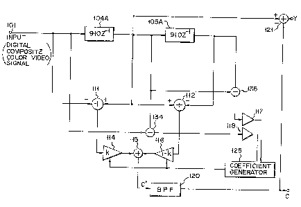
As shown in Fig. 1, the present invention uses a
signal from a first section 101 receiving a digital com-
posite color video input signal, an output signal of a
second section 104A which delays the signal from Eirst
section 101 by a time corresponding to one scanning line
(a one-scanning-line time), and an output signal of a
third section 105A which further delays the output
signal of second section 104A by the one-scanning-line
time. A signal representing a difference between the
input signal to first section 101 and the output signal
of second section 104A is taken out of an adder 111 and
then applied to a first coefficient multiplier 114. A
signal representing a difference between the output
signals of second and third sections 104A and 105A is
taken from an adder 112 and then applied to a second
coefficient multiplier 116. Further, a difference
signal of the input signal to first section 101 and the
output signal of second section 104A is derived from a
subtracter 134 and then applied to a first absolute-
value circuit 118. A subtracter 134 provides and
applies a difference signal of the ou~put signals of
second and third sections 104A and 105A to a second
absolute-value circuit 117. And, output signals of
13~25~
-- 8
first and second absolute-value circuits 118 and 117
are applied to a coefficient generator 125. Coefficient
generator 125 decides as to which of the absolute-value
outputs exhibits a higher vertical correlation, or
which of the absolute-value outputs indicates a smaller
interline difference, and increases the weighting coef-
ficient in one of first and second coeEficient multi-
pliers 114 and 116 that corresponds to the higher
vertical correlation. Output signals of first and
second coefficient multipliers 114 and 116 are added
together in an adder 115. The resultant sum signal is
used at least as a chrominance signal component C'
separated from the digital composite signal.
The luminance signal (Y) component can be derived,
like the prior art, from an adder 121 as a difference
signal of an output signal of a bandpass filter 120 con-
nected to receive the chrominance signal component C'
from adder 115 and the output signal from second section
104A.
The arrangement can avoid problems of the dot
crawl and the like because the weighting coefficient
for separation between lines on which the frequency of
vertical components in the luminance signal is low
(vertical correlation is high) is made larger than
that for separation between lines on which the frequency
of the vertical components in the luminance signal is
high.
13~025'7
An embodiment oE the present lnvention will be
described hereinafter.
Referring now to Fig. 2, an analog composite color
video signal applied to an input terminal 101' is sub-
jected to analog-to-digital (A/D) conversion in an A/D
converter lOlB responding to a clock signal of 4fsc pro-
vided from a clock generator lOlA, and then applied to
a unit delay element 102 adapted for one-clock-time
delay and an adder 110. An output signal of unit delay
element 102 is transmitted through a unit delay element
103, a delay element 104 adapted for 908-clock-time
delay, unit delay elements 131, 132, a 908-clock delay
element 105 and unit delay elements 106, 107 to an adder
113.
A first processing uni-t A is comprised of unit
delay elements 102, 102 and an adder 110. An output
signal of processing unit A is fed to a second process-
ing section B providing a time delay of one scanning
line. The second processing section B is comprised of
delay element 104 and unit delay elements 131 and 132
and adder 133. An output signal of second processing
section B is applied to a third processing unit C having
a time delay of one scanning line. The third processing
section C is comprised of delay element 105 and unit
delay elements 106 and 107 and adder 113.
An output signal from an intermediate output of the
first processing section A, that is, an output between
~3~
-- 10 --
unit delay elements 102 and 103 and an output signal
from an intermediate output of the second processing
section B, i.eO, an output between unit delay elements
131 and 132 are applied to an adder 111 to produce their
difference signal. The difference signal is applied to
a coefficient multiplier 11~ to be weighted by a control
signal from a coe~ficient generator 125 described later
and then applied to an adder 115.
An output signal from an intermediate output of the
second processing section B, specifically the output
between unit delay elements 131 and 132 and an output
signal from an intermediate output of the third pro-
cessing section C, specifically an output between unit
delay elements 106 and 107 are applied to an adder 112
to produce their difference signal. The difference
signal is applied to a coefficient multiplier 116 to be
weighted by a control signal from coefficient generator
125 and then applied to adder 115.
To detect two lines having a higher vertical corre-
lation therebetween among three scanning lines in onefield in the input video signal, the following processes
are performed.
The input signal to unit delay element 102 and the
output signal from unit delay element 103 are applied to
adder 1~0, and the resultant sum signal is applied to
an input of a subtracter 134. The other input of sub-
tracter 134 is supplied with a sum signal of the input
~3~(~2S7
signal to unit delay element 131 and the output signal
from unit delay element 132 provided from adder 133.
The sum signal is also applied to an input of a sub-
tracter 135 the other input of which is connected to
receive a sum signal of the input signal to unit delay
element 106 and the output signal from unit delay ele-
ment 107 provided from adder 113. The output signals of
- subtracters 134 and 135 are applied to absolute-value
circuits 117 and 118, respectively. The outputs of
absolute-value circuits 117 and 118 are coupled to
coefficient generator 125~
Coefficient generator 125 detects smaller one of
the absolute values provided from the absolute-value
circuits, that ls, two lines, among three lines, which
has a higher vertical correlation and then correspon-
dingly controls the weighting coefficient of coefficient
multiplier 114 or 116. In this case, the weighting
coefficient associated with the two lines having a
higher vertical correlation is made larger. When one
of coefficient multipliers 114 and 116 has a coeEficient
of k, the other has a coefficient of l-k. The output
signals of coefficient multipliers 114 and 116 are added
together in adder 115 and then applied to a bandpass
filter 120 for separation and extraction of the chromi-
nance signal C through an output terminal 124. The
chrominance signal C is applied to an adder 121 to be
subtracted from the output signal of unit delay element
~3~025'7
131. Thus, adder 121 separates the luminance signal Y
from the composite signal and provides it to an output
terminal 123. It is to be noted that the clock signal
oE 4fsc is also applied to delay elements 102-107, 131
and 132 from clock generator lOlA.
The operation of the embodiment ~ill be described
with reEerence to Figs. 2 and 3.
It is assumed that the digital composite color
video signal to input terminal 101 is sampled by clocks
of 4fsc as in the prior art which are synchronized with
the I and Q axes. If S3 is the digital composite color
video signal, Sl the output of unit delay element 102,
S4 the output of unit delay element 103, S7 the output
of delay element (line memory) 104, S0 the output of
unit delay elemen-t 131, S8 the output of unit delay
element 132, S5 the output of delay element 105, S2 the
output of unit delay element 106, and S6 the output of
unit delay element 107, then data arrangements on scan-
ning lines Ya, Yb and Yc will be indicated as shown in
Fig. 3.
Adder 110 performs an operation of S3 + S4 to
output signals on the scanning line Ya, and adder 133
performs an operation of S7 + S8 to provide signals on
the scanning line Yb. Adder 113 performs an operation
of S5 + S6 to provide signals on the scanning line Yc.
The outputs of adders 134 and 135 will be
Dl = Ya - Yb
:13~0.Z57
- 13 -
D2 = Yc - Yb
Coefficient generator 125 examines D1 and D2 to
provide the coefficient k represented by
k = f(Dl, D2)
The conversion can be realized by, for example,
k = D2 / (Dl + D2)
1 - k = Dl / (Dl + D2) (k < 1)
or by
k = f (Dl - D2)
The output signal C' of adder 115 representing the
chrominance signal component C will be given by
C' = k(S0 - Sl) + (1 - k) (S0 - S2)
The weighting coefficients k and l-k are determined by
an output signal of coefficient generator 125. The pur-
pose of control of the weighting coefficients is, as
shown in Fig. 4, to make small the weighting coefficient
for the operational output between two adjacent lines
(Ya, Yb; Yb, Yc) having a greater difference in lumi-
nance level (a lower vertical correlation) among three
scanning lines (Ya, Yb, Yc), while to make large the
weighting coefficient for the operational output between
the two adjacent lines (Yb, Yc; Ya, Yb) having a smaller
difference in the luminance level (a higher vertical
correlation). Owing to the control of the weighting
coefficients as described above -the dot crawl and the
cross-color can be reduced, improving the picture
quality.
~130~25Y~
- 14 -
As described above, -the present invention is
arranged to increase, in separating the chrominance
signal from the composite signal, a proportion of the
separated output (chrominance signal output) by the use
of signals on two adjacent lines having a hlgher ver-
t.ical correlation among signals on three scanning lines.
Therefore, the leak of the C signal into the ~ signal
and the reverse leak can be suppressed, providing high-
quality pictures.