Note : Les descriptions sont présentées dans la langue officielle dans laquelle elles ont été soumises.
~3V~7~
-1- RCA 84,965
DEFLECTION CURRENT CORRECTION CIRCUIT
This invention relates to an arrangement of a
television apparatus for varying a deflection current in
response to a control signal. The control signal may be
generated, for example, when the deflection current is not
synchronized to a synchronizing signal.
Typically, a control signal that is nominally at
a vertical rate controls a vertical sawtooth signal
generator of a vertical deflection circuit. The control
signal determines the period of a deflection current in a
vertical deflection winding that, in turn, determines the
amplitude of the vertical deflection current.
In a television apparatus that utilizes a control
signal generator such as, for example, an integrated
circuit (IC) TA7777 made by Toshiba, Japan, (the Toshiba
IC) for producing the control signal, the frequency of the
control signal may he lower during free running, or
unsynchronized operation of the vertical deflection circuit
than during synchroniæed operation. Free running operation
occurs when a vertical synchronizing signal is decoupled
from the control signal generator that generates the
aforementioned control signal. The synchronizing signal is
decoupled, for e~ample, during an interval in which a new
channel is selected for viewing. The lower frequency of
the control signal may cause the amplitude o~ the vertical
deflection current, if not corrected, to be larger than
during normal op~ration.
When an on-screen display feature (OSD) is
utilized in the television receiver, the video information
containing the charaGters to be displayed is applied to the
corresponding guns of a cathode ray tube (CRT) of the
receiver synchronously with the vertical control signal
that was mentioned before. During, for example, channel
change and/or during auto programming, the vertical
synchronizing signal is decoupled from the control signal
generator. This causes the amplitude of the vertical
deflection curxent to be larger. The synchronizing signal
is decoupled from the control signal generator in order to
13(~ 4Z
-2- RCA 84,965
reduce noise related disturbances during, for example, the
channel selection interval. The increased amplitude of the
deflection current, if not corrected, may result,
disadvantageously, in the repositioning of OSD characters
toward the top of the screen. Characters of the OSD near
the top of the screen may be moved partially or completely
o~f the CRT screen viewing area.
In accordance with an aspect of the invention, a
second control circuit is provided that is responsive to a
second control signal. The second control signal is
indicative of the occurrence of intervals when ~he first
control signal is at a lower frequency than during
synchronized operation, or unsynchronized to the vertical
synchronizing signal. The second control signal causes a
reduction in the amplitude of a sawtooth signal that is
produced in the sawtooth signal generator. Therefore, the
rate of change of the ~ertical deflection current is
reduced for maintaining its amplitude closer to that during
normal operation. Conse~uently, when the OSD characters are
displayed, the vertical deflection current, even though it
is at a lower frequency than in normal operation, is at a
level ~hat is close to that obtained during normal
operation. The result is that the OSD characters are
displayed close to their normal synchronized operation
positions.
~ n accordance with another aspect of the
invention, an arrangement responsive to a control signal
generates a deflection current in a deflection winding.
When the deflection current is synchronized to a
synchronizing input signal the contxol signal is at a first
state. When the deflection current is free running, the
control signal is at a s~cond state. The control signal
causes the amplitude of the deflection current to be
substantially the same when it is synchronized as when it
is free running.
In the Drawing:
~3007~Z
,--
-3- RCA 84,965
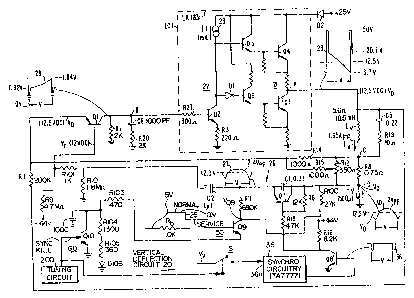
FIGURE 1 illustrates a vertical deflection
circuit with vertical current correction arrangement
embodying an aspect of the invention; and
FIGURES 2a and 2b illustrate waveforms useful in
explaining the operation of the circuit of FIGURE 1.
In the illustrated vertical deflection circuit 20
of FIGURE 1, for a television receiver or a video display
apparatus, a vertical deflection winding ~ is coupled to a
vertical amplifier output stage 21 at an output terminal A.
A current sampling resistor R8 is coupled to deflection
winding ~ at a terminal C, and a DC blocking and S-shaping
capacitor Cv is coupled to resistor R8 at a terminal D.
Vertical output stage 21 includes a top amplifier
transistor Q4 coupled to a ~25V DC supply via a diode D2
and a bottom amplifier transistor Q3 coupled to a ground
reference potential point through a resistor. A driver
stage 22 is coupled to output stage 21 for driving the
output stage at a vertical rate in a sawtooth manner to
gene~ate a sawtooth vertical deflection current iv in
vertical deflection winding Lv.
Drlver skage 22 includes an inverting amplifier,
driver transistor Q2, and a current source 23 coupled to
the collector o~ the tr~nsistor. Driver transistor Q2
drives t~p output transistor Q4 via a noninverting buffer
transistor Q5, and drives bottom output transistor Q3 via
an inverting stage Ul and a noninverting bufer transistor
Q6. The driver and output stages may be incorporated into
an integrated circuit, IC 1, such as the LA7831,
manufactured by Sanyo Corporation.
To generate a vertical sawtooth current iv in
vertical deflection winding ~, a vertical ramp generator
26 generates a downwardly going vertical ramp voltage 27
that is AC coupled by a capacitor C2 to the base of an
error amplifier transistor Ql. Error amplifier transistor
Ql inverts vertical ramp voltage 27 to develop a vertical
input voltage 28 across a collector load resistor Rl of
transistor Ql. Input voltage 28 is applied to an input
~,
~3~:)7~2
- -4- RCA 84,965
terminal B of driver stage 22 that is coupled to the base
of inverting amplifier transistor Q2 via a resistor R27.
Vertical input voltage 28 progressively increases
the conduction of driver stage 22 during the vertical trace
interval, progressively shunting more of current I1,
developed by current source 23, away from top output
amplifier Q4 and buffer Q5. During the first half of
trace, output transistor Q4 is conducting, to couple the
+25V supply to vertical deflection winding LV via diode D2.
A decreasing vertical deflection current iv flows in
deflection winding LV and cha.rges DC blocking capacitor Cv
from the +25V supply via transistor Q4~
During the second half of vertical trace, dri-~er
transistor Q2 has been made sufficiently conductive by
input voltage 28 to turn off top output transistor Q4 and
turn on bottom output transistor Q3. DC blocking capacitor
CV discharges to ground via vertical deflection winding LV
and transistor Q3, thereby generating the negative sawtooth
portion o~ vertical de~lection current iv.
To initiate the vertical retrace interval, input
voltage 28 turns off driver transistor Q2, thereby turning
off bottom output transistor Q3 and turning on top output
transistor Q4. Conventional vertical retrace circuitry,
not illustrated .in the FIGURES, pxovides for the retrace of
vertical de~lection current iv.
The operation of output stage 21, in response to
vertical input voltage 28, develops a vertical output
voltage 29 at output terminal A that is applied to vertical
deflection winding Lv. The DC level, V0, established at
output terminal A, also establishes substantially the same
DC level at terminals C and D. Vertical deflection current
iV generates an AC sawtooth voltage between terminals C and
D, across sampling resistor R8, and generates a parabolic
component 30 to the voltage VD developed across DC blocking
capacitor Cv.
A DC negative feedback loop from output terminal
A to input terminal B stabilizes the average DC operating
voltage level at terminal A. The DC voltage at terminal A
13~()7~z
-5- RCA 84,965
is coupled via terminal C to the emitter of error amplifier
transistor Q1 to establish the DC voltage of the emitter at
voltage level V0. Voltage level V0 is compared with a
reference voltage level Vr that is developed at the base of
transistor Ql by voltage dividing resistors R9, R101 and
R10. The level of input voltage 28 is controlled by the
conduction of transistor Ql for stabilizing the DC voltage
level V0 at an operating level that is approximately lVbe
above reference voltage level Vr.
AC negative feedback for scan linearization is
provided by coupling the AC sawtooth voltage developed
across sampling resistor R8 to the emitter of error
transistor Q1 via a voltage dividing network comprising
potentiometer R12 and resistors R14 and R15. The AC
sawtooth voltage at the emitter of error transistor Q1 is
compared against vertical ramp voltage 27 that is AC
coupled through capacitor C2 to the base of the transistor
in order to develop the AC component of i.nput voltage 28.
Deflection current amplitude is adjusted by adjusting the
wiper arm of potentiometer R12.
Ramp generator 26, that develops ramp voltage 27,
comprises an RC lntegrating network, capacitor C1 and a
resistor R11. During normal operation, resistor R11 has a
t~rmi~al that is coupled to ground via a series arrangement
of a transistor Q9, that is conductive during normal
operation, a resistor R103 and a transistor Q10, that is
also conductive during normal operation. A reset switch,
transistor Q7, is coupled across capacitor C1. Voltage VD
developed across DC blocking capacitor Cv is applied to the
integrating network of capacitor C1 and resistor R11. The
DC component o~ voltaye VD is integrated by capacitor C1 to
generate a downwardly-going ramp of voltage across resistor
Rll. The AC, parabolic component of voltage VD is
integrated by capacitor Cl to provide S-shaping of the ramp
voltage across resistor R11.
To initiate vertical retrace, ramp capacitor Cl
is discharged by making reset transistor Q7 conductive. A
vertical reset pulse 36, ~Jenerated by a vertical
13~ 2
-6- RCA 84,g65
synchronization circuitry 136 such as, for example, the
aforementioned Toshiba IC, is applied to the base of a
transistor Q8, making the transistor nonconductive during
the short reset pulse interval. The collector of
transistor Q8 is coupled to a +44V supply by a resistor
R16. The collector of transistor Q8 is DC coupled to the
base of reset transistor Q7 via a resistor R18. Negative
going reset pulse 36 is inverted by transistor Q8 and
applied to the base of transistor Q7, to turn transistor Q7
on and discharge capacitor Cl. The sharp increase in ramp
voltage 27 when capacitor C1 is discharged is coupled to
the base of error amplifier transistor Q1 and turns the
transistor off to initiate the vertical retrace interval.
A capacitor C5 in series with a xesistor R19
across deflection winding LV damps deflection winding
resonances. A resistor R7 is coupled between output
terminal A and the emitter of error amplifier transistor Q1
to compensate for horizontal rate pickup by vertical
de1ection winding Lv. A capacitor C6 in series with a
res.istor R20 is coupled between input terminal B and ground
to roll of~ the gain at higher frequencies to prevent
deflection circuit high fre~uency oscillation.
During service mode operation of the television
receiver, used, for e~ample, when color temperatuxe is to
be manually adjusted, or when degaussing is required, the
raster is collapsed ~ertically by disabling vertical
deflection circuit 20. Accordingly, a service mode
switching circuit 50 disables the generation of vertical
deflection current when the service mode of operation is
asserted. Service mode switching circuit 50 includes
service mode switching transistor Q9 having its collector
coupled to an end terminal of resistor Rll that is remote
from the junction between capacitors C2 and C1. A resistor
R100 is coupled between terminal D of capacitor Cv and the
collector of transistor Q9. The emitter of transistor Q9
is coupled to ground through resistor R103 and transistor
Q10.
~3007~2
. . .
-7- RCA 84,965
During the normal mode of television receiver
operation, a mode-switching signal 25, that may be
conventionally generated, is in the high state, maintaining
transistor Q9 in saturated conduction. Therefore, ramp
generator 26 operates in the manner described before.
To assert the service mode of television receiver
operation, mode-switching signal 25 is switched to the low
state to cutoff conduction in transistor Q9. With
transistor Q~ cutoff, the current path via resistor R11 for
charging capacitor C1 is opened. Therefore, capacitor Cl
can no longer be charged and the plate of capacitor C2 that
is coupled to capacitor Cl will be at the level of voltage
VD. Conse~uently, generation of ramp voltage 27 ceases.
Resistor R100 prevents leakage current from charging
capacitor Cl.
Due to the DC negative feedback provided by
resistors R14, R15 and R12, the DC voltage at each of
terminals A, C and D will be maintained at approximately
+12.5 volts, that is approximately e~ual to reference
voltage level Vr plus one Vbe voltage of transistor Ql.
Therefore, capacitor Cv will be maintained charged to
approximately ~12.5 volts during service mode of operation.
Conseguently, when normal mode of operation is resumed, the
txansient supply current via diode D2 is, advantageously,
smaller than if capaci~tor Cv were not already charged.
An AC feedback loop path between the input and
output of IC 1 includes capacitor Cl in parallel with
switching transistor Q7. Because transistor switch Q7
operates during both the normal and service modes of
operation, the frequency response characteristic of the AC
feedback loop is substantially the same in both modes of
operations. Therefore, advantageously, the frequency
response characteristic, once optimized for normal mode of
operation, is unlikely to cause instability in the AC
feedback loop during the service mode of operation.
When a user initiates a channel selection chan~e
command to a tuning circuit 200, a conventional OSD
character generator, not illustrated, is lctivated to
13~ 2
-8~- RCA 84, 965
generate channel number display at an edge of the screen.
Simultaneously, a control signal SYNC KILL is generated by
turning circuit 200 that causes a switch S to decouple a
vertical synchronizing signal Vv from a synchronizing
signal receiving terminal 136a of synchronizing circuitry
136. Decoupling signal Vv is desixable since signal Vv,
during a transition interval when the channel is changed
might contain noise that might adversely affect the
deflection currents. Conseguently, free running operation
occurs in circuitry 136 that causes the frequency of signal
36 to become lower.
FIGURES 2a and 2b illustrate waveforms useful for
explaining the operation of the circuit of FIGURE 1.
Similar s~mbols and numerals in FIGURES 1, 2a and 2b
indicate similar items or functions. As shown by the dash
line in FIGURE 2b, the interval between successive vertical
reset pulses 36 is e~ual to, for example, 296H during free
running operation, whe~e H is the horizontal period. In
contrast, such interval is equal to 262.5H in normal
operation. Therefor~, the amplitude of deflec~ion current
iv of FIGURE 1 havin~ a trace portion that is shown in
FIGURE 2a may becom~ larger during ~ree running operation,
if not corrected. Without correction, the level of vertical
deflection current iv at time tl during free running
operation that occurs when OSD characters be~in to be
displayed would be larger than during normal operation.
Therefore, the OSD characters that are to be displayed in
the vicinity of the top of the screen would move to the top
of the screen or even completely off the screen.
In accordance with an aspect of the invention,
signal SYNC KILL is coupled to the base of transistor Q10
of a correction circuit 60. Signal SYNC KILL causes
transistor Q10 to become nonconductive when free running
operation occurs in circuitry 136. Consequently, resistors
R104 and R105 of correction circuit 60 are interposed
between resistor R103 and ground. The result is that a
voltage VQg at the collector of transistor Q9 increases
from, for example, -tO. 4 volts, occurring during n~rmal
-` ~3~ 42
-9- RCA 84,965
operation, to +2.13 volts, occurring when signal SYNC KILL
is generated. The increase in voltage VQg is determined by
the aforementioned resistors that form a voltage divider
with resistor Rb, through the base-emitter junction of
transistor Q9. Resistor Rb couples through such voltage
divider signal 25 that is at approximately 5 volts to the
base of transistor Q9. Except during the previously
described service mode operation, signal 25 is at
approximately +5 volts.
The increase in voltage VQg causes the rate of
change of vertical ramp voltage 27 to decrease.
Consequently, the increase in amplitude of deflection
current iv due to the lower fre~uency of reset pulse 36 is
prevented. The result is that at time tl of FIGURE 2a,
occurring when the OSD characters begin to be displayed,
deflection current iv is at a level close to that during
normal operation. Therefore, advantageously, the
positioning of the OSD characters remains substantially
the same as in normal operation even though the deflection
current frequency is lower.