Note : Les descriptions sont présentées dans la langue officielle dans laquelle elles ont été soumises.
13~Z~
- 1 - 03LO-06090
CONTROL CIRCUITS, ELECTRONICALLY
COMMUTATED MOTO~ 8YSTEN~ AND MET~OD8
FIELD OF THE INVENTION
This invention relates in general to control
circuits and application systems for dynamoelectric
machines and other electrical systems and to methods of
their control and operation. More particularly, this
invention relates to control circuits for electrical
apparatus and systems such as electronically commutated
motor systems, electronically commutated motor systems
themselves and methods of control and operation.
13~1~Z~
03LO-06090
BACRGRO~JND OF THE INVENTION
Without limiting the intended applications of
the invention for all electrical systems which need
improved control circuits and methods of operation and
all applications generally to which the features and
advantages of the invention commend it, the background
of the invention is discussed in regard to a relatively
specific example of controls for electronically
commutated motors.
While conventional brush-commutated DC motors
may have advantageous characteristics, including
convenience of changing operational speeds, there may
be disadvantages such as brush wear, electrical loss,
noise and radio frequency interference caused by
sparking between the brushes and the segmented
commutator, which may limit the applicability of
such brush-commutated DC motors in some fields such
as the automotive and domestic appliance fields, for
JF~pd ~ ~ 03-LO-6090
GEN 9211 ~3U~ 0 PATENT
example. Electronically commutated motors, such as brush-
less DC motors and permanent magnet motors with electronic
commutat~on, have now been developed and generally are
believed to have the above discussed advantageous charac-
teristics of the brush-commutated DC motors without many of
the disadvantage~ thereof whl}e al80 having other important
advantagez. TheEe electronically commutated motors are
advantageously employed, for instance, in air conditioni~g
f~r coolin~ and warming of vehicular compartments and also
in laundering apparatus. While there are some losses
engendered by electronic switching of an electronically
commutated motor, these are negligible compared to brush
losses and rheo~tat losses in prior art variable speed
systems.
Some circuits and electronically commutated
motors are disclosed in coassigned Wright U.S. Patent
4,162,435, in coassigned Boyd U.S. Patent 4,52~,485, in
coassigned Boyd et al. U.S. Patents 4,540,921, 4,636,936
and 4,642,S36, in Alley U.S. Patent 4,2S0,544, Alley et al.
U.S. Patent 4,250,435, Bittin~ et al. U.S. Patent
4,500,821, in Young U.S. Patent 4,642,537 and Archer U.S.
Patent 4,686,436. While the aforementioned coassigned
patents, for instance, undoubtedly illustrated many
features, it is believed that the control circuits for
electronically commutated motors in general and for
other applications could be even further improved, as
well as the methods of control utilized therein.
Further improvements in control systems,
electronically commutated motor systems, and
30 methods of control and operation can
beneficially contribute to more wide-spread use of
such motors in their various applications. For
example, improvements directed to increased noise
JFHpd 03-LO-6090
GEN 921i 1 3~ O PATENT
immunity, fail-safe operation, economy of manufacture and
greater versatility of respon e to various signal condi-
tions generally would be desirable.
Summary of the Invention
A~mong the ob~ects of this invention are to pro-
vide improved control circuitry -or electrical systems,
improved electronically commutated motor systems, and
improved methods of control and operation which provide
increased noise immunity; to provide improved control cir-
cuitry for electrical systems, improved electronically
commutated motor systems, and improved methods of control
and operation having enhanced fail-safe features: to pro-
vide improved control circuitry for electrical systems,
improved electronically commutated motor systems, and
improved methods of control and operation having greater
versatility of response to various signal conditions; and
to provide improved control circuitry for electrical sys-
tems, improved electronically commutated motor systems, and
improved methods of control and operation that are reliable
and economical to manufacture.
Generally and in one form of the invention, a
control circuit is provided for an electronically commu-
tated motor which has a rotatable assembly and further has
a station~ry assembly with a plurality of wind$ng stages
having terminals for energization, and switching means for
applying a voltage to one or more of the terminals of the
winding stages at a time and commutating the winding stages
in a preselected sequence to rotate the rotatable assem-
bly. A preselected sequence of winding stages are left
correspondingly unpowered so that a plurality of the wind-
ing stages are unpowered at some time. The winding stages
JFHpd ,. 03-LO-6090
GEN 9211 ~3~ PATENT
generate back emf signals and also couple electrical sig-
nals from each energized winding stage to the unpowered
winding stages which signals can interfere with detection
of back emf for position sensing purposes. The control
circuit includes a first circuit for selecting at least two
of the unpowered winding stages which have electrical sig-
nals coupled to them that have a predetermined relationship
in polarity and magnitude. A second circuit produces an
electrical output from the voltages on the winding stage
terminals of the winding stages selected, so that the elec-
trical signals coupled from each energized winding stage
are substantially canceled when they have the predetermined
relationship while the back emf is preserved for position
sensing substantially free from interference from the elec-
trical signals that are coupled from each energized windingstage to the unpowered winding stages.
In general, another form of the invention is a
control circuit including a commutating circuit that
applies a voltage from the power source to energize an
electronically commutated motor so that a winding stage is
temporarily powered and another winding stage is temporar-
ily unpowered, terminates the application of voltage to a
temporarily powered winding stage in response to a first
control signal and advances in a commutation sequence in
response to a second control signal to effect rotation of
the rotatable assembly. Another circuit responds to the
terminal voltage of a temporarily unpowered winding stage
to produce a sensing output which i~ a function of angular
position of the rotatable asæembly. A first electrical
level is established to represent a first position of the
rotatable assembly at which a temporarily powered winding
stage is to be deenergized, and a second electrical level
represents a second position of the rotatable assembly at
which the commutating circuit is to advance in the
JFHpd , O 3-LO-6 0 9 0
GEN 9211 ~ PATENT
sequence. A comparing circui~ compares the sensing output
with the first and second electrical levels to produce the
first and second control signals for the commutating cir-
cuit when the first and second positions are respectively
reached by the rotatable assembly.
In qeneral, still another form of the invention
is a control circuit including a set of bistables for the
winding stages of an electronically commutated motor. Each
bista~le has a first state for powering a respective wind-
ing stage in response to a first control signal and a sec-
ond state for terminating the application of voltage to the
same winding stage in response to a second control signal.
Also included is further controlling circuitry for generat-
ing a sequence o~ electrical signals to determine which of
the bistables shall receive the first control signal and
which of the bistables shall receive the second control
signal, and the controlling circuitry is responsive to a
third control signal to advance in the sequence. Sensing
circuitry responds to the terminal voltage of at least one
temporarily unpowered winding stage to produce a sensing
output which is a function of angular position of the
rotatable assembly. A comparing circuit compares the sens-
ing output with first, second and third electrical levels
to respectively produce the first and second control sig-
nals for the bistables and the third control signal for thefurther controlling circuitry.
Generally, yet another form of the invention is a
control circuit with a sensing circuit responsive to the
terminal voltage of at least one winding stage for produc-
ing a sensing output which is a function of angular posi-
tion of the rotatable assembly. The sensing output has a
variable frequency which depends on the speed of the rotat-
able assembly. A comparing circuit compares the sensing
output with a first electrical level to produce a first
JF~pd 03-LO-6090
~EN 9 211 ~3~1z~a~) PATENT
control signal for commutation purposes. A second circuit
generates a varying second electrical level representing a
varying value beginning with an initial value, resets the
second electrical level to the initial value in response to
the first control signal and resumes generating the varying
second electrical level which thereby depends on the fre-
quency of the sensing output that results from the speed of
the rotatable assembly. The comparing circuit also com-
pares the sensing output with the second electrical level
to produce a second commutation control signal.
In general, an additional form of the invention
is a control circuit including a shift register circuit
having a serial input, a set of parallel inputs, a control
input to select the serial input or parallel inputs for
entry, and outputs for supplying a parallel digital signal
representing a commutation in the sequence. The shift
register circuit is to be protected from electrical inter-
ference which could cause the outputs to supply a parallel
digital signal unrepresentative of any commutation in the
se~uence. Another circuit supplies a parallel digital
signal representing a particular commutation in the
sequence to the set of parallel inputs of the shift regis-
ter circuit. The shift register circuit has its control
input connected to respond to at least one of the outputs,
and its serial input connected to respond to at least one
of the outputs so that if any unrepresentative parallel
digital signal appears at the outputs which does not repre-
sent any commutation in the sequence, the unrepresentative
parallel digital signal is replaced by another parallel
digital signal representing a commutation in the sequence
when the shift register circuit is next clocked.
Generally, another additional form of the inven-
tion is a control circuit for an electronically commutated
motor and is used with a position sensor for repeatedly
JFHpd 03-LO-6090
GEN 9211 ~3~z~ PATENT
generating a sensing signal generally representative of
rotat~on of the rotatable a~ embly. The con~rol circuit
has a circult for frequency dividing 06cillator pul~es tc
supply lower freguency pulses. The frequency dividing
circuit has a reset input for repeated resetting by the
sensing signal, so that when the rotatable assembly is
turning at least as fast as a predetermined spin rate the
sensing signal is generated at a repetition rate for reset-
ting that prevents the lower frequency pulses from being
supplied and otherwise allows the lower frequency pulses to
be supplied when the sensing signal is generated at a lower
repetition rate. Another circuit responds to the lower
frequency pulses when they occur to produce an electrical
signal generally representing an accumulated number of the
lower frequency pulses. A further circuit compares with a
predetermined value the electrical signal representing the
accumulated number of the lower frequency pulses, and sup-
plies a disabling signal for a predetermined period of time
for disabling commutation of the motor after the predeter-
mined value is reached by the electrical signal, to preventenergization of the motor during that predetermined period
of time.
In general, a further form of the invention is a
control circuit for apparatus to be powered by a power
source having a source voltage which is supposed to be in a
range between a lower voltage limit and a higher voltage
limit. The control circuit includes a first circuit for
deriving a first voltage from the source voltage as a first
function of the source voltage and a second circuit for
deriving a second voltage from the source voltage as a
second function of the source voltage, wherein the second
voltage is equal to the first voltage only at the lower
voltage limit and the higher voltage limit. A comparing
J~Hpd f ' 4C~ 03-LO-6090
GEN 9211 3L3~Z PA~ENT
circuit is connected to the first and second deriving cir-
cuits and compares the first and second voltages to produce
a control signal for the apparatus to be powered, the con-
trol signal indicating wheth~r the source voltage is within
or outside the range.
Generally, a yet further form of the invention is
a control circuit for an electronically commutated motor
that is to be compatible with alternative external control
devices indicating desired speed. The control circuit
includes a circuit for generating pulse width modulated
pulses to control switching devices for the motor, the
pulses modulated in width as a function of an analog speed
control signal. A second circuit supplies the analog speed
control signal with respect to a common to the circuit for
generating the pulse width modulated pulses. The second
circuit has a capacitor and an active device circuit with
an input resistively connected to a terminal for a voltage
source, the input also for connection to any of the exter-
nal control devices, and an output resistively connected to
the capacitor so that the capacitor develops the analog
speed control signal when the input of the active device
circuit is connected to any of the following external con-
trol devices: A) pulse generator with a duty cycle repre-
sentative of desired speed, B) variable voltage source
representative of desired speed, or C) variable resistance
representative of desired speed.
In general, a further additional form of the
invention is a control circuit for use with an electrical
load and a power source with a switching section therebe-
tween, wherein the power source bas a source voltage whichis subject to a transient substantially in excess of a
normal value of the source voltage. The control circuit
includes a first control section for producing a varying
first electrical signal for the switching section to
JFHpd O 3 -LO- 6 0 9 0
GEN 9211 ~L3~L;240 PATENT
repeatedly connect and disconnect ~he electrical load to
and from the power source in normal operation. ~urther
included is a second control section responsive to the
transient in the source voltage when the transient occurs
and connected to the first control section for overriding
the first control section so that the f irst electrical
si~nal is forced to a level to make the switching section
connect the electrical load to the power source for the
duration of the transient.
Generally, a yet further additional form of the
invention is a control circuit for use with an electroni-
cally commutated motor and solid state switches for apply-
ing a source voltage to one or more of the terminals of the
winding stages at a time, the solid state switches having a
saturation voltage depending on current flowing through
them when conducting. The control circuit includes a com-
mutating circuit for generating commutation pulses in a
preselected sequence to make the solid state switches con-
duct and commutate the winding stages in a preselected
sequence to rotate the rotatable assembly. The repetition
rate of the commutation pulses is related to the speed of
the rotatable assembly. Further circuitry responds to the
commutation pulses to supply a variable electrical level
which varies in magnitude as a function of the repetition
rate of the commutation pulses, the electrical level repre-
senting a current limit for the motor as a function of
motor speed. A disabling signal is produced for the commu-
tating circuit when the saturation voltage across the
switches exceeds the variable electrical level in magni-
tude, whereby current for the motor is limited as a func-
tion of motor speed.
The invention comprehends electronically commu-
tated motor systems improved to include control circuits as
described above and other improvements. Also, various
JF~pd `~, 03-LO-6090
GEN 9211 ~3~J~Z40 PATENT
methods of the invention inYolve steps for accomplishing
various aspects of control and operation of the circuits
described above.
Other objects and features will be in part appar-
ent and in part pointed out hereinafter.
Brief Description_of the Drawings
Fig. 1 is a block diagram of an electronic con-
trol circuit of the inventlon in an electronically commu-
tated motor system of the invention:
Fig. 2 is a schematic diagram of inventive cir-
cuitry in part of the system of Fig. l;
Fig. 3 is a set of voltage-versus-time diagrams
of back EMP waveforms for the motor of Figs. 1 and 2,
illustrating inventive operations of the control circuit of
Fig. 1 according to a method of the invention;
Fig. 4 is a voltage-versus-time diagram of inte-
grator output X in the circuits of Figs. 1 and 2, illus-
trating further inventive operations of the control circuit
of Fig. 1 according to a method of the invention:
Fig. 5 is a schematic diagram of further inven-
tive circuitry in part of the system of Fig. l;
Figs. 6A and 6B are a pair of voltage-versus-time
diagrams of waveforms of advancement capacitor voltage in
the circuit of Fig. 5, illustrating further inventive oper-
ations of the control circuit of Fig, 1 according to a
method of the invention;
Fig. 7 is a voltage-versus-time diagram of wave-
forms including advancement capacitor voltage, voltages
from Firing Angle and Termination Angle potentiometers, and
integrator output X at a low motor speed and a higher motor
speed in the circuit of Fig. 5, illustrating further inven-
tive operations of the control circuit of Fis. 1 according
11
JFHpd 03-LO-6090
GEN 9 211 13~1Z40 PATENT
to methods of the invention, the diagram having a second
vertical axis for rotor angular position corresponding to
the vertical axis for voltage:
Fig. 8 is a schematic diagram of further inven- !
tive circuitry in a commutation section of the system of
Fig. l;
Fig. 9 is a simplified electrical diagram of an
electronically commutated motor showing mutually coupled
signals from an energized winding into two unpowered wind-
ings, to illustrate an interference cancellation process ofa further preferred embodiment of the invention;
Pig. 10 is a schematic diagram of inventive cir-
cuitry for position sensing and other functions which
implements interference cancellation according to Fig. 9;
lS Fig. 11 is a set of voltage-versus-time diagrams
of back EMF waveforms for the motor of Figs. 1 and 2, hav-
ing the vertical axis sense of each waveform inverted rela-
tive to Fig. 3, and illustrating inventive operations of
the control circuit of Pig. 10 according to a method of the
invention;
Fig. 12 is a schematic diagram of an alternative
position counter of the invention using a shift regis,er
approach for increased immunity from electrical interfer-
ence, for use with the circuit of Fig. 10~
Pig. 13 is a schematic diagram of a blocked rotor
protective circuit of the invention and pulse width modula-
tion circuitry of the invention, for use with the circuit
of Pig. 12
Figs. 14 and 15 are voltage-versus-time diagrams
of output Q10 of a counter in the circuit of Pig. 13 illus-
trating further inventive operations:
Pig. 16 is a diagram of output Q10 of the counter
in the circuit of Fig. 13 versus motor rotation rate,
illustrating inventive operations:
JF~pd 13~ lZ40 03-Lo-6090
GEN 9211 ~ PATENT
Fig. 17 is a voltage-versus-time diagram of a
voltage YC2 in Fig. 13 representing an accumulation of
pulses from output Q10 in the circuit of Fig. 13 and illus-
trating further inventive operations, the time scale of
Fig. 17 being longer than that of Figs. 14 and 15;
~ig. 18 is a voltage-versus-time diagram, to the
same time scale as Fig. 17, of a disabling signal output
DISl/ in Fig. 13 and illustrating further inventive opera-
tions:
Fig. 19 is a schematic diagram of an under-
overvoltage circuit of the invention operating by methods
of the invention and for use with the circuitry of Fig. 13;
Fig. 20 is a diagram of voltage versus source
voltage of various voltages in the circuit of Fig. 19,
illustrating further inventive operations;
Fig. 21 is a diagram of voltage versus source
voltage of an under-overvoltage disabling output UVOV/ for
the circuit of Pis. 19, illustrating more inventive opera-
tions;
Fig. 22 is a schematic diagram of a universal
input speed control circuit of the invention operating by
methods of the invention and for use with the circuitry of
Fig. 19:
Figs. 23 and 24 are a flow diagram of method
steps of some preferred methods of operating the control
circuitry and electronically commutated motor system of the
earlier Figures;
Fig. 25 is a schematic diagram of inventive com-
mutation logic, inventive load dump transient protective
circuitry, and inventive autoprotective overcurrent sensing
circuitry operating by methods of the invention and for use
with the circuitry of Figs. 10, 12 and 13;
Fig. 26 is a schematic diagram of inventive power
supply circuitry operating by methods of the invention and
JFHpd 3~Z40 03-LO-6090
GEN 9211 PATE~T
for use with the circuitry of ~igs. 10, 12, 13, 19, 22 and
25; and
F~g. 27 is a flow diagram of method steps of some
preferred methods of operating the control circuitry and
electronically commut~ted motor system o Figs. 10 and 25.
Corresponding reference characters indicate cor-
responding parts throughout the several views of the
drawings. A symbol ~/~ herein represents the logical com-
plement of a digital logic signal wh~re the context indi-
cates.
Detailed DescriPtion of Preferred Embodiments
In Fig. 1 an electronically commutated motor 1 hasa stationary armature or assembly 2 with a core 3 and
energizable wye-connected winding stages 4 such as the three
lS winding stages also shown in Figs. 1 and 2 of Canadian Patent
1,199,997, issued January 28, 1986. The winding stages 4 are
arranged to establish a predetermined number P o~ magnetic
poles, where P = 8, for instance. A permanent magnet rotor
5, illustratively having 8 magnets with alternating north and
south poles facing the stationary assembly 2, is adapted to
rotate as a rotatable assembly in response to the magnetic
poles estab~lished by the winding stages. (An alternative
motor with inside-out construction, not shown, has an
exterior permanent magnet rotor and an interior stator with
the winding stages wound thereon.)
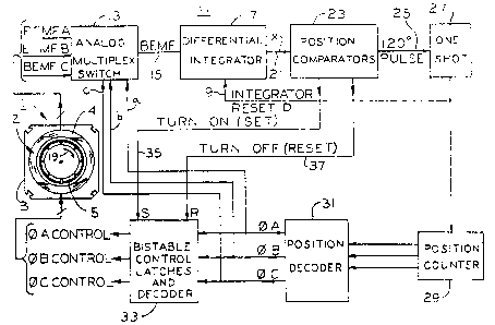
A control circuit 11 in Fig. 1 is connected to
the motor 1 to form an electronically commutated motor
system. Control circuit 11 has an analog multiplexer 13
connected to the winding stages 4 that switches a selected
one or more sensing lines for back EMF (counter electromotive
force) designated BEMF A, BEMF B, and BEMF C. The
14
JF~pd 03-LO-6090
GEN 9211 ~3-~J1240 PATENT
analog multiplexer 13 operates in response to three posi-
tion control signals OA, OB, and OC on respective lines a,
b, and c. The one or more selected sensing lines from
analog multiplexer 13 are switched to a BEMF path 15 to a
differential integrator 17. The integrator 17 is reset by
an integrator reset signal D on a line 19 at each commuta-
tion. The output of the inteqrator 17 is a voltage X which
varies as a function of angular position 19 of the rotata-
ble assembly 5 of the electronically commutated motor 1.
The output of integrator 17 is supplied on a line
21 to position comparators 23. There, it is determined
when commutation should advance in a sequence of commuta-
tion by supplying a pulse on a line 25 to a one shot cir-
cuit 27. The one shot circuit 27 produces a pulse which
acts as reset signal D on line 19 to reset the integrator
17. This same pulse D is also provided to a position
counting circuit 29 which provides three outputs to a posi-
tion decoder circuit 31. The position decoder circuit 31
supplies the position control si~nals OA, OB, and OC as
three decoded outputs for the analog multiplexer 13 and for
a further bistable circuit 33 that has more decoding cir-
cuitry and a set of control latches, or flip-flops. Bista-
ble circuit 33 provides control signals OA Control, OB
Control, and OC Control for switching the winding stages 4
and thereby energizing motor lr
The latches in bistable circuit 33 are set and
reset in response to TURN ON signals on a set S line 35 and
TURN OFF signals on a reset R line 37. The TURN ON and
TURN OFF signals are provided from position comparators
circuit 23. In this way the initiation and termination of
control signals OA Control, OB Control, and OC Control are
precisely and adjustably determined by means of circuits 23
and 33.
GEN 9211 13~:1Z40 03-Lo-6090
In Fig. 2 examples of analog multiplexer 13 and
differential integrator 17 of Fig. 1 are detailed wlth
their connections to winding stages 4. Individual winding
stages 4A, 4B, and 4C are connected together at a neutral
S 4N which is connected to a power supply or source (not
shown) of a voltage B~. Each of the winding stages 4A, 48,
and 4C have respective winding stage ~erminals 4AT, 43T,
and 4CT, where it is to be understood that Uterminal~
refers to a conductive portion at an end of a windin~
stage, and does not necessarily denote a separate electri-
cal component. A snubber circuit 45 partially dissipates
and partially returns power to supply voltage B+ from the
terminals of winding stages 4A, 4B and 4C when commutation
occurs. An example of snubber circuit 45 is described in
connection with Fig. 10.
A set of switches 43A, 43B, and 43C are connected
respectively between the winding stage terminals 4AT, 4BT,
and 4CT and a common w~ich completes a return to the souroe
of voltage. The switches connected to the winding stages
in this way provide a half bridge configuration. In this
way when any of control signals OB CONTROL, OA C~NTROL and
OC CONTROL on lines B, A, and C goes high, the correspond-
ing electronic switch 43B, 43A, or 43C is made conductive
and energizes its corresponding winding stage 4B, 4A, or
4C.
The winding stage terminals 4AT, 4BT, and 4CT are
also connected to corresponding voltage dividers 47A, 47B,
and 47C for back EMF sensing. A suitable voltage division
ratio is provided to make the outputs of the voltage divid-
er.s compatible in level with integrated circuitry. BackEMF signals BEMF A, BEMF B, and BEMF C are thus supplied on
correspondingly marked lines to three analog switches 13A,
13B, and 13C which operate as analog multiplexing circuit
13. Analog switches 13C, 13A, and 13B are controlled by
16
JFHpd ~3~. ~1240 03-LO-6090
GEN 9211 ~ PATENT
signals OC, OA, and OB of ~ig. 1 on lines c, a, and b
respectively. Only one of the switches in the analog mul-
tiplexer 13 is activated at any given time for an unpowered
winding stage in the embodiment of F~g. 2, while none, one
S or two of lines B, A and C may be high simultaneously to
control switches 43B, 43A and 43C.
The outputs of the three analog switches 13A,
13B, and 13C are connected together to a resistor 49 which
is connected to the inverting ~_n input of a differential
operational amplifier 55. Operational amplifier 55 is
connected to amplify the difference be~ween the back EMF
voltage at the output of the analog multiplexer 13 and a
voltage which is proportional to the voltage B+ at neutral
4N by the same proportion as voltage dividers 47A, 47B, and
47C provide for the voltages at terminals 4AT, 4BT and
4CT. A voltage divider 51 provides the voltage division
for the neutral voltage from source voltage B+ which is
connected through the voltage divider 51 and a resistance
network 53 to the non-inverting ~+~ input of the operation-
al amplifier 55. A Zener regulated voltage VREF is sum-
med by resistance network 53 with the approximated neutral
voltage from voltage divider 51 to bias the input voltage
about halfway between ground and supply voltage Vcc for
operational amplifier 55 so that the input common mode
voltage is within the operating range of amplifier 55.
The output of operational amplifier 55 is resis-
tively connected to the inverting ~-~ input of a second
operational amplifier 57 which is connected as an integrat-
ing amplifier with the amplifier 57 having an integrating
capacitor 59 connected between the output and ~he inverting
input. The inverting input is also connected by an analog
switch 61 to a positive voltage Vcc that exceeds VREF
for resetting purposes. Analog switch 61 is made conduc-
tive when integrator reset voltage D goes high on line 19.
JF~pd 3~z 03-LO-6090
GEN 9211 1 40 PATENT
Operational amplifier 57 is also supplied with the Zener
regulated voltage VREp at its non-inverting ~+a input to
reference it compatibly with the operational amplifier 55.
A potentiometer 63 trims the offset voltage for integrating
amplifier 57 so that with zero differential voltage on the
input side of the integrator, integration is negligible in
either direction. Output X of the integrator operational
amplifier 57 supplies position comparators 23 of FigO 1 as
described later hereinbelow in connection with Fig. 5. In
this way, motor 1 has winding stages 4 connected at a neu-
tral 4N. A voltage divider 51 for the neutral 4N provides
a voltage generally proportional to the voltage on the
neutral to integrator 17 to produce sensing output X.
Analog switches 13A-C act as an example of an electroni-
cally controlled switch means responsive to the electrical
signals from a circuit (e.g. 31) for controlling them.
Switches 13A-C selectively connect at least one unpowered
winding stage at any given time to the integrator 17 for
producing sensing output X.
Fig. 3 shows waveform diagrams correcponding to
the voltage at neutral 4N less the voltages at terminals
4AT, 4BT, and 4CT respectively. In Fig. 3 the voltages are
120 electrical degrees apart and have identical waveforms.
Each waveform is high when its winding stage is energized
by switch 43A, 43B or 43C to make its terminal voltage
low. Each waveform is low during an unpowered period when
the corresponding winding stage is unpowered and the ter-
minal voltage exceeds the neutral voltage. Substantially
linear ramp segments join the low and high voltage seg-
ments. The actual positions on the horizontal time axis
which the various electrical degree positions occupy and
the number of cycles of waveforms which occur in a given
period of time depend on the speed of the rotatable assem-
bly.
18
GEN 9211 i3~Z40 03-LO-6090
In this embodiment the voltage (back emf) during
an unpowered period is utilized for position sensing pur-
poses. Zero electrical degrees (0) and 180 points on the
ramps correspond to particular angular positions of the
rotor where the terminal voltage of the winding stage 4A is
equal to the neutral voltage (iOe., where the back emf is
zero), and the actual number of these angular position6
spaced around the circular bore of the motor depends on the
number of poles of the motor.
For purposes of the embodiment of Fig. 2, each
360 degree repetition period in Fig. 3 is divided or parti-
tioned into three 120 segments for Firing Range, Turn Off
Range and Sense respectively. The Firing Range commences
60 electrical before a zero electrical degree 0 point is
reached by the rotatable assembly. An instant or position
ON for first actual application of voltage to a winding
stage is established anywhere in the Firing Range, such as
a few degrees after the 0 point as shown. An instant or
position OFF for termination of voltage to a winding stage
is established anywhere in the Turn Off Range, such as
about 150 as shown. The winding stage is unpowered during
the entire 120 of the Sense period, which is used in this
embodiment for obtaining back EMF for position sensing
purposes.
Circuits 17, 23, 27, 29 and 31 of Fig, 1 estab-
lish the timing of the various operations in Fig. 3 to
properly select winding stages by analog multiplexer 13 for
voltage sensing and to make bistable circuit 33 apply volt-
age and terminate voltage to the appropriate winding stages
at desired times. ~uring each 120 segment the control
circuit 11 measures the back EMF of one motor winding,
energizes the second winding and turns off the third wind-
ing. In this way, the back EMF from one winding is used to
control the other two windings.
19
JFE~pd .. ~, 03--LO-6090
GEN 9 211 ~ J 1;~40 PATENT
This illustrative form of method o~ partitioning
allows the turn on (firing) angle for a particular winding
stage to be selected to occur within an adjustment range of
+60 from the back EMF zero crossing of that winding
stage. The turn off angle is independently adjustable from
+60 to 180 referenced to the back EMF zero crossing. In
other words, the circuit advantageously provides indepen-
dent controi of the turn on and turn off angles of energi-
zation of the winding stage~. Note that these selections
can allow two pha~es to be energized simultaneously (over-
lapped firing) or can allow some dead time wherein all
three windings are deenergized. With speed feedback, an
example of which is described later hereinbelow, the firing
angle is advantageously changed dynamically as a function
of speed. The ability to control these angles dynamically
opens another degree of freedom to optimize electronically
commutated motor performance parameters such as torque
ripple, e~ficiency, speed and power.
In Fig. 4 integrator output signal X rises posi-
tive. Signal X has a first generally parabolic-curved part
65 resulting from integration of part 66 of the linear ramp
in the Sense period of Fig. 3. Then signal X has a second
generally linear ramp portion 67 resulting from integration
of a generally constant or flat portion 68 of the back EMF
in the Sense period of Fig. 3.
In Fig. 5 signal X is supplied to a comparator 71
at its non-inverting ~+~ input. When signal X rises to a
predetermined level V120 established by a potentiometer
73 at the inverting ~-- input terminal of comparator 71,
~0 then comparator 71 supplies an output high to one shot
circuit 27 causing that circuit 27 to produce a pulse D
having a predetermined duration as illustrated in Fig. 4.
The duration of pulse D is established by a resistor 77 and
capacitor 79 in Fig. 5 associated with one shot circuit
J~Hpd 13~1Z40 03-LO-6090
GEN 9211 PATENT
75. A re~ulated voltage VR is provided for potentiometer
73 by means of a Zener diode 81 and a resistor 83 connected
between common and a terminal for voltage B+.
Further in Fig. 5, two additional comparators 91
and 93 compare the signal X with a Turn On voltage level
VON established by a potentiometer 95 at its wiper or
adjustable point, and a Turn Off voltage level VOFp
established and adjustable independently by a potentiometer
97. Thus, when integrator output X, which is provided to
non-inverting inputs of comparators 91 and 93, exceeds the
Turn Off level VOFF then the output of comparator 91 goes
high. When integrator output X exceeds the Turn On level
VON established by potentiometer 95, the output of com-
parator 93 goes high.
In the embodiment of Figs. 2 and 5, the opera-
tional process thus starts with the analog multiplexer
selecting that motor winding stage which is entering its
Sense period wherein it is not energized and will not be
energized during the 120 Sense period. The selected back
EMF signal is then integrated to remove (by averaging)
mutually coupled noise resulting from the switching in the
other windings and to yield a voltage which is related to
angular position. This ~position~ voltage is compared with
three reference voltages as discussed above to yield three
comparator signals. One signal marks the 120 period, one
marks the turn on or firing angle and the third marks the
turn off angle. ~ach time the 120 marker occurs, it trig-
gers the one shot 27 which advances position counter 29 of
Fig. 1 and rese~s the integrator 17. One version of the
position counter 29 is a two bit counter which has three
states. The binary counter outputs are decoded by position
decoder 31 to provide three signals which mark the particu-
lar 120 segment of the back ENF being operated on. Only
one of the three is active at one time. These signals are
21
GEN 9211 13~i240 03-LO-6090
asserted to the analog multiplexer 13 to select the proper
motor winding stage for sensing and to provide control
windows for turning on and off the three winding stages 4A,
43 and 4C.
A Set output for initlating pulse energization
for each latest winding stage is produced by an AND-gate
101. A Reset output for termination of the pulse energiza
tion of each winding stage to be deenergized is supplied by
an AND-gate 103. AND-gate 101 has a first input connected
to the output of VON comparator 93, and AND-gate 103 has
a first input connected to the output of VOpF comparator
91. An inverter 105 is connected from the D output of
one-shot 27 to a second input of each of AND-gates 101 and
103. AND-gates 101 and 103 are enabled by inverter 105 at
all times except when the D output of one-shot 27 is high.
This embodiment does not recognize any occasion for initia-
tion or termination of winding stage energization during
the D output, and so the presence of inverter 105 enhances
reliability and noise immunity. Thus, when integrator
output X exceeds the Turn On level VON established by
potentiometer 95, comparator 93 output goes high and AND
gate 101 output goes high to produce the Set signal. When
output X exceeds the Turn Cff level VOFF established by
potentiometer 97, the output of comparator 91 goes high
producing a high Reset output from AND-gate 103.
Integrator 17 of Fig. 1 thus acts as an example
of a means responsive to the terminal voltage of a tempo-
rarily unpowered third winding stage for producing a sens-
ing output which is a function of angular position of the
rotatable assembly. Other circuits besides an integrator
could also exemplify such means. Potentiometers 95, 97 and
73 act as an example of a means for establishing a first
electrical level representative of a first position of the
rotatable assembly at which voltage is to be applied to a
GEN 9211 13C~lZ4~ 03-LO-6090
second winding stage, a second electrical level representa-
tive of a se~ond position of the rotatable assembly at
which voltage to a first winding stage is to be terminated,
and a third electrical level representative respectively of
a third position of the rotatable asse~bly a~ which a com-
mutating circuit (e.g. in Fig. 8) is to advance in
sequence. Further, comparators 93, 91 and 71 act as an
example of a means for comparing the sensing output with
the first, second and third electrical levels to produce
first, second and third control signals (e.g. Set, Reset,
and D) for the commutating circuit when the first, second
and third positions are respectively reached by the rotata-
ble assembly.
A further advantageous speed variable operation
is provided by a circuit 131 of Fig. 5 for making circuit
11 of Fig. 1 a speed compensated firing circuit. Circuit
131 changes the firing angle (angular position of the rotor
at which the turn on signal is generated to energize a
winding stage) as a preadjustable function of speed to
yield better motor performance. Fine angle compensation as
a function of speed is also possible using this circuit
131, which provides independent adjustment of turn on
angle, turn off angle, and advancement control of these
angles as speed increases. For example, higher speed and
shaft power are obtained in some motor contexts by advanc-
ing the firing angle determined by voltage VON as the
speed increases. This means that voltage VON should
decrease as speed increases, as provided by circuit 131.
In circuit 131 a capacitor 133 produces a ramp
voltage Vc in response to a PNP transistor 135 acting as
a current source. The capacitor 133 is connected between
the collector of transistor 135 and common. The base of
transistor 135 is held at an approximately constant voltage
by means of a voltage divider 137 connected across zener
23
JF~pd :13~:1240 03-Lo-60gO
GEN 9211 PATENT
diode 81. The emitter of transistor 135 is connected by a
variable resistor 139 to zener diode 81. In this way, a
constant current level, provided by transistor 135 acting
as a charging circuit, is adjustable by variable resistance
139, and voltage Vc across charging capacitor 133 ramps
up linearly.
Each time one-shot 27 produces signal D to
advance in the commutation sequence, the capacitor voltage
VC is reset to zero by discharging capacitor 133 in
response to the signal D whereupon the charging circuit
135, 139 resumes charging capacitor 133. As the capacitor
voltage rises, so does the turn on voltage VoN~ As the
motor runs faster the capacitor is reset more often causing
the peak capacitor voltage to be less. This causes the
angle of energization to advance as speed increases.
It should be noted that advancement angle and
angle advance herein are distinct concepts from advancing
in sequence. Advancing in se~uence continually changes
signal patterns in control circuit 11 for different winding
stages as the rotatable assembly or rotor turns. Advance-
ment angle as used herein is an angle difference in elec-
trical degrees between the physical rotor position for zero
back emf and a rotor position for which the control circuit
11 is set to initiate energization of a latest winding
stage. Angle advance as used herein is a relative advance-
ment angle between the physical rotor position for energi-
zation of a winding stage at low speeds and a rotor posi-
tion for which the control circuit 11 is set to initiate
energization of a latest winding stage at a given speed.
Capacitor 133 with its voltage Vc is further
connected to the base of a PNP buffer transistor 141 con-
nected in a common collector configuration as a high impe-
dance buffer circuit connected across capacitor 133 for
producing a buffer output that at least initially rises
24
JFHpd 13(~1~4~) 03--LO-6090
GEN 9 211 PATENT
with capacitor voltage Vc. A selector switcb 143 has its
movable member connected to the lower voltage end of poten-
tiometers 95 and 97. In a Speed Independent mode switrh
143 connects the potentiometers 95 and 97 to common.
S Potentiometers 95 and 97 supply the voltages VON and
VOFF as preadjustable constant voltage levels independent
of the speed of motor 1 by voltage-dividing the regulated
voltage of Zener diode 81 in the Speed Independent mode.
In a Speed Variable mode of selector switch 143
the lower voltage ends of potentiometers 95 and 97 are
connected to the emitter of buffer transistor 141. The
collector of transistor 141 is connected to common~ A
zener diode 145 is connected across the emitter and collec-
tor of buffer transistor 141 and acts to limit the buffer
output provided it reaches a predetermined level VH.
Each potentiometer 95 or 97 acts as a voltage division
means connected between the power source and capacitor 133,
with comparators 93 and 91 having their inverting inputs
connected to the ad~ustable points cf potentiometers 95 and
97 respectively.
As shown in Figs. 6A and 6B the Turn On level
VON and Turn Off level VOFF developed by potentiometers
95 and 97 vary with motor speed in the Speed Variable mode,
while the 120 degree level V120 remains the same. For
example, in Fig 6A the emitter voltage of transistor 141
increases with the ramp voltage Vc across capacitor 133
of Fig. 5 until the emitter voltage reaches a relatively
high level at zener voltage VH of zener diode 145,
because a substantial period of time is consumed in turning
the rotatable assembly 5 of motor 1 of Fig. 1 through a
full 120 electrical. Therefore, the Turn On and Turn Off
voltage levels are relatively high in Fig. 6A at slower
speeds. Zener diode 145 thus restrains the electrical
~3~1~4~
JF~pd 03-LO-6090
GEN 9211 PATENT
level of the emitter voltage from varying beyond a prede-
termined value provided it reaches the predetermined value
before the control signal D next occurs. In this way, the
emitter voltage reaches and is limited to the predetermined
value at speeds of the rotatable assembly less than a pre
determined sp~ed.
On the other hand, at higher speeds as shown in
Fig. 6B, a shorter length of time is required to turn the
rotatable assembly through 120 and there is insufficient
time for capacitor 133 to develop a voltage as high as
VH. Instead, a lower peak voltage VL is developed, and
VL varies with speed. The charge on capacitor 133 of
Fig. 5 is thereupon discharged by a discharging NPN tran-
sistor 151 which has its collector and emitter connected
across capacitor 133 and which is turned on through a base
resistor 1~3 each time signal D from one shot 27 goes
high.
As just discussed, the lower voltage ends of
potentiometers 95 and 97 only reach the voltage VL and
they develop lower ON and OFF voltages of Fig. 6B which are
equal to
VON = VC + kl(VR vc) (1)
VOFF = VC + k2(VR vc) (2)
where VON is the Turn On voltage, VOFF is the Turn Off
voltage, Vc is the voltage across capacitor 133 at a
given time, VR is the zener voltage of zener diode 81,
and kl and k2 are the preadjusted voltage division con-
stants for potentiometers 95 and 97 respectively.
Since potentiometers 95 and 97 are independentlY
adjustable, The Turn On voltage can either exceed or be
exceeded by the Turn Off voltage. When the Turn On voltage
26
JFElpd ~3~1240 03-Lo-6090
GEN 9211 PATENT
exceeds the Turn Off voltage, one winding stage is deener-
gized before the next one is energized, leaving a time
period or gap when none of the winding stages are ener-
gized. When the Turn On voltage is exceeded by the Turn
Off voltage, one winding stage is energized before the next
one is deenergized, leaving a time period of overlap when
two of the winding stages are energized.
Circuit 131 of Fig. 5 thus generates a varyiny
electrical level representing a varying value beginning
with an initial value. Transistor 151 responds to the
control signal D for resetting circuit 131 so that the
electrical level is returned to the initial value, where-
upon circuit 131 resumes generating the varying electrical
level. That level thereby depends on the frequency of the
sensing output X that results from the speed of the rotata-
ble assembly. The comparators 93 and 91 compare the sens-
ing output X with the electrical level from each of poten-
tiometers 95 and 97 to produce Set and Reset control
signals for the commutating circuitry.
Two circuits like 133, 135 and 139 can be pro-
vided for potentiometers 95 and 97 respectively, for inde-
pendent adjustment of angle advancement or retardation per
unit of speed change. Still other embodiments can use a
single potentiometer in place of potentiometers 95 and 97
to produce a voltage which is provided to comparators 91
and 93 as both the OFF and ON voltage.
Fig. 7 further illustrates the operations of the
Speed Variable mode. A charging curve of capacitor voltage
VC ramps up to a plateau at voltage VH. Corresponding
curves for potentiometer 95 voltage VON per ~quation (1)
and potentiometer 97 voltage VOFF per Equation (2) have
generally higher initial ramps and final voltage plateaus
than voltage Vc but have smaller ramp slopes. Superim-
posed on the curves for VOFF and VON are two alternate
JFHpd 13~1240 03-LO-6090
GEN 9211 PATENT
curves of integrator output X for an example of a high
speed and a low speed respectively.
At a low speed as shown in Fig. 7, the integrator
output XLOw rises from zero, intersects the plateau level
of VON at time LToN~ then intersects the illustra-
tively higher plateau level of VOFF at time LToFF~
and eventually reaches constant voltage level V120
~potentiometer 73 of Fig. 5) at a time LT120. At a
high speed the inteqrator output XHIG~ rises much more
rapidly from zero, intersects the ramp portion of VON at
time HToN~ then intersects the illustratively higher
OFF at time HTOFF, and soon reaches
constant voltage level V120 at a time HT120.
Due to the integration of back EMF by integrator
17, the output XHIG~ or X~ow is directly related to the
electrical degrees of rotor an~ular position, as indicated
by the parallel vertical axes labeled ~Electrical Degrees~
and ~Voltage~ in Fig. 7. The Firing An~le of the motor for
purposes of Fig. 7 is regarded as the rotor angular posi-
tion in electrical degrees corresponding to the voltageplateau level of Turn On voltage VoN~ In other words, at
slow speeds, each winding stage is energized at the rotor
angular position represented by the Firing Angle. At
increasingly higher speeds, however, the intersection of
the integrator output X moves leftward along the plateau of
VON and down the ramp part of VoN/ so that energization
of each winding stage is initiated at progressively earlier
angular positions of the rotor. At the rotor speed which
produces the example integrator output XHIGH, an angle
advance aON represents the difference between the Firing
Angle and the actual angle at which energization is initi-
ated at that rotor speed.
A Termination Angle of the motor is herein
regarded as the rotor angular position in electrical
28
JP~pd ~3~1Z40 03-LO-6090
GEN 9211 PATENT
degrees corresponding to the voltage plateau level of Turn
Off voltage VOFF. (Strictly speaking the Termination
Angle is 120 plus the Y axis value of electrical degrees
corresponding to voltage VOFF in Fig. 7.) At slower
speeds, each winding stage is deenergized at the rotor
angular position represented by the Termination Angle. At
increasinqly higher speeds, and analogously to firing, the
intersection of the integrator output X moves leftward
along the plateau of VOpF and down the ramp portion of
VOFF, so that energization of each winding stage is ter-
minated at progressively earlier angular positions of the
rotor relative to the Termination Angle. At the rotor
speed which produces the integrator output XHIGH, a ter-
mination angle advance value aOFF represents the differ-
ence between the Termination Angle and the actual anqle atwhich energization is terminated at that rotor speed.
It is desirable to make the advancement or angle
advance change in a controlled manner with rotor speed.
For example, in some applications it is desirable to make
the advancement or angle advance increase relatively slowly
with increase of speed at lower speeds and to increase more
rapidly with increase of speed at the higher speeds. In
one embodiment a tachometer circuit detects the speed,
feeds it to a lookup table which supplies a value of
advancement (or else firing angle advanced by the angle
advance) which then is fed for summation (or directly) to
the comparator 93 input. In another embodiment a motor
current sensor detects the current (which represents the
torque loading) and the tachometer circuit detects the
speed. Both the speed and torque information are fed to
the lookup table (implemented either in custom-designed
hardware or in software in a computer) which supplies the
value of advancement (or else firing angle advanced by the
29
JF~pd 13~ 4C~ 03-Lo-6090
GEN 9211 PATSNT
angle advance) which then is fed for summation (or direct-
ly) to the comparator 93 input. In other embodiments, a
resistance-capacitance charging circuit provides a voltage
which is used to modify the potentiometer output to the
comparator. In the embodiment shown in the drawings, for
~nstance, a line~r ramp charging circuit with zener cla~p
prov~des the appropriate fir1ng ~nyle for low speeds and
then increases the advancement at the higher speeds. Por
even more pronounced rate of increase of advancement at the
higher speeds, a charging exponential (Cl + C2e~t/RC)
curve for VON and VoFp is obtained by eliminatiny tran-
sistor 135 and voltage divider 137. In this latter embodi-
ment~ capacitor 133 is charged directly from variable
resistance 139 to economically obtain a charging exponen-
tial curve. In still another embodiment a computer istriggered by one shot 27 to produce a series of digital
values which are converted to analog form by a digital-to-
analog converter to produce any curve desired. It is con-
templated that other embodiments within the inventive scope
also produce desired advancements as a function of speed
and/or torque so that the needs of particular motor appli-
cations are met.
In Fig. 5, variable resistor 139 provides a fine
adjustment of the angle advance as speed increases. In the
discussion hereinbelow, the angle advance is analyzed gen-
erally for a relatively broad class of embodiments and the
function of variable resistor 139 is derived as a special
case.
Assume a relationship X(A) between the integrator
output X and actual rotor position A in electrical àegrees,
where position A equals the product of rotor speed w multi-
plied by time t. For illustration, the relationship X(A)
is assumed linear in the region of intersection with the
ramping parts of VOFF and VON in Fig. 7. The slope of
JF~pd ~3~1Z40 03-LO-6090
GEN 9211 PATENT
the integrator output graphed as a function of time in ~ig.
7 varies as a function o~ speed w. However, the derivative
of integrator output with respect to angle A can be assumed
constant with a value sl.
s At slower speeds, comparator 91 senses when the
following equation is satisfied
X(Ao) ~ V~ + kl(VR-V~) (3)
where Ao is the Firing Angle and V~ is the limit as
time goes to infinity of a voltage Vc(t) provided to
potentiometer 95 in Speed Variable mode.
At higher speeds, comparator 91 senses the inter-
section of integrator output X with the VON output as
follows:
(Ao aON) Vc(t) + kl(VR-Vc(t)) (4)
where aON is angle advance and Vc is capacitor 133
voltage or some substitute produced by other means such as
a computer. Subtracting Equation (4) from Equation (3)
yields
X(Ao)-xlAo-aoN) = (l-kl)(VH VC( )
Since X(A) is linear in the range of interest, the expres-
sion on the left side of Equation (5) is the constant s
multiplied by angle advance aON. Substituting and
rearranging yields an equation for angle advance aON:
ON ((l kl)/sl)V(t) (6)
where aON is angle advance, kl is the voltage division
constant of the potentiometer, sl is the slope of the
31
JF~pd 13~1240 03-~0-6090
GEN 9211 PA~ENT
relation of integrator output X to rotor position in elec-
trical degrees, and V(t) is a voltage function of time of
intersection where V(t) = VH-Vc(t). This voltage func-
tion V(t) is entirely general and does not depend on par-
ticular circuitry of circuit 131~ E~uation (6) is thusdescriptive of microprocessor-based firing advance cir-
cuits, capacitor-based circuits as in Fig. 5 and other
embodiments. The time t of intersection is inversely
related to speed w according to the relationship
( O aON)/w (7)
where Ao is Firing Angle and aON is the angle advance.
In practicing the invention in this aspect, the
skilled worker either assumes the function V(t) to be lin-
ear or decaying exponential in time as described above, or
maps V(t) by measurements as described next.
A laboratory measuremer.t method for mapping the
function V(t) uses the control circuit (such as the embodi-
ment of Fig. 5 in Speed Independent mode) to determine the
desired advance angle values at several speeds w of the
motor. At each speed solve for t using eguation (7) and
solve for V by rearranging equation (6) as
ONsl/(l kl) (8)
The corresponding values of V and t thus obtained map the
function V(t) which then is generated by analog circuitrY
designed to model it or by a microprocessor programmed to
generate it. Where it is desired to include motor torque
as well as motor speed in the determination of the angle
advance aON, the torque dependence of the Firing Angle is
determined by measurements which then are implemented in a
lookup table for the value kl.
32
JF~pd ~ 3~i ~Z~ o 3-LO-6090
GEN 9211 PATENT
In the special case of circuit 131 of Fig. 5, the
resistance R of variable resistor 139 is related to the
slope (herein 52 volts per second) of the capacitor 133
voltage Vc in Pig. 5. This slope is given by
S2 = VR/~RC) ~g)
where VR is the zener voltage of zener diode 81, R is the
effective resistance including variable resistor 139 in
series with capacitor 133, and C is the capacitance of
capacitor 133. The voltage across capacitor 133 is given
by
VC ' S2t (10)
where 52 is slope and t is time in seconds.
Substituting Equation (10) into Equations (1) and
(2), the Turn On and Turn Off voltages are given by
VON = (l-kl)52t + klVR (11)
VOFF = ll-k2)S2t + k2VR (12)
Finally, substituting E~uations (9) and (10) with (5) and
rearranging yields
aON ((l-kl)Jsl)(VH - VRt/RC) (13)
where t is given by Equation 7.
In Fig. 8 commutation circuitry for operating
winding stages 4 of Fig. 1 includes counter 29, decoder 31,
and latches and decodins circuitry 33. Co~nter 29 is
illustratively realized by a 3-state circuit comprised of a
13~ 0
JFHpd 03-LO-6090
GEN 9211 PATENT
first JK flip-flop 161 and a second JK flip-flop 163.
Flip-flops 161 and 163 both have signal D connected to
their clock CK inputs. The Q output of flip-flop 161 is
connected to its K input. The Q output of flip-flop 163 is
connected to its own R input and to the J input of flip-
flop 161. A not-Q output of flip-flop 161 is connected to
a J input of flip-flop 163. The set S and reset ~ inputs
of fl$p-flops 161 and 163 are all tied to common and are
inactive. Thus, for example, if the flip-flops 161 and 163
initially have their Q outputs low (first counter state
00), then their not-Q outputs are high. When signal D
clocks both flip-flops, the high not-Q output of flip-flop
161 is supplied to the J input of flip-flop 163 setting the
Q output of flip-flop 163 high (second counter state 10).
Clocking the flip-flops a second time with signal D causes
the now-high Q output of flip-flop 163 at input J of flip-
flop 161 to set the Q output of flip-flop 161 high. Simul-
taneously, the Q output of flip-flop 163 is reset low
because of the high at the K input of flip-flop 163 at this
time (third counter state 01). Clocking the flip-flops a
third time with signal D resets the Q output of flip-flop
161 because of the high at the K input of flip-flop 161 at
this time, returning the flip-flops to first counter state
00 .
A decoding network comprised of the three AND-
gates 165, 167, 169, and inverters 171 and 173 produces
outputs a, b, and c from AND-gates 169, 167, and 165
respectively. AND-gates 169, 167, and 165 respectively
decode the first (00), second (10) and third counter state
(01) to produce a high output a, b, c when each state
occurs. One and only one of these a, b, c outputs is high
during each arc of rotation of the motor from commutation
to commutation, and the output which is high remains high
34
GEN 9211 ~3V1240 03-LO-6090
throughout the entirety of a given arc between commuta-
tions.
A set of bistables (~S flip-flops or latches)
181, 183 and 185 initiate and terminate energization pulses
and establish their pulse width on lines A, B, and C to the
circuit of Fig. 2. Each bistable 181, 183 and 185 has a
first state (high) for powering a respective winding stage
4A, 4B or 4C in response to the Set control signal and a
second state (low) for terminating the application of volt-
age to the respective winding stage in response to theReset control signal. Counter 29 and decoder 31 act as a
control for generating ~ sequence of electrical signals at
outputs a, b, c to determine which of the bistables
receives the Set control signal and which of ~he bistables
receives the Reset control cignal. The counter 2g responds
to signal D as a third control signal to go to the next
state and make outputs a, b, c advance in the sequence upon
each occurrence of signal D.
In Fig. 8, AND-gates 191, 193, and 195 are all
enabled at a first input by the Set control signal. AND
gates 191, 193, and 195 are also respectively connected at
a second input to outputs b, c, and a from AND-gates 167,
165, and 169 respectively. As discussed hereinabove, only
one of these AND-gate outputs a, b, and c is high at any
one time. Therefore, only one corresponding bistable 185,
lal, or 183 becomes set during any one sequence interval
for the appropriate winding stage which is to be ener-
gized.
Similarly, the Reset control signal enables AND-
gates 201, 203 and 205 at the same time but only one ofthose AND-gates 201, 203, and 205 is qualified by an output
c, a, or b respectively. In this way, a flip-flop lBl,
183, or 185 which was set just prior to the present
sequence interval is reset in the present interval. Thus,
JF~lpd 1.3c:1~Z4(~ 03-LO-6tl90
GE~ 9211 PATENT
output a allows the Set signal to set the line C latch and
allows the Reset signal to reset the line B latch. Output
b allows the Set signal to set the line A latch and allows
the Reset signal to reset the line C latch. Output c
allows the Set signal to set the line B latch and allow~
the Reset signal to reset the line A latch, whence the
sequence repeats. Over a series of intervals, a repeating
sequence of pairs of the bistables have one bistable in
each pair set and the other bistable in each pair reset.
Thus, the circuitry of Fig. 8 acts as an example
of a commutating means for applying a voltage from a power
source to energiæe the motor so that a winding stage is
temporarily powered in response to a Set control signal in
a first sequence interval and another winding stage is
temporarily unpowered, initiating energization of another
winding stage in response to another occurrence of the Set
control signal in the next sequence interval and terminat-
ing the application of voltage to the temporarily powered
winding stage in response to a Reset control signal and
advancing in the sequence in response to a sequence control
signal (e.g. signal D) to effect rotation of the rotatable
assembly. Independently adjustable potentiometers 9S and
97 of Fig. 5 vary the first and second electrical levels
for Turn On and Turn Off relative to each other so that at
least two of the winding stages either variably overlap in
a time period of energization or variably in time terminate
the voltage applied to one of the winding stages before a
time when the second of the two windin~ stages has voltage
applied to it. In other words, depending on the setting of
the potentiometers (or of fixed voltage dividers which can
be used), two of the winding stages may be energized at
once during an overlap period in the half-bridge circuit of
Fig 2, or there may be a gap in energization when none of
the winding stages is energized.
3~
JF~pd ~ ~ 03-LO-6090
GEN 9211 3~4~ PATENT
Fig. 9 illustrates a noise cancellation process
of the invention applied in a motor with winding stages 4A,
4B, and 4C connected together at neutral 4N which is con-
nected to supply volta~e B+. Two of the winding stages 4B
and 4C are caused to be unenergized when a switch S is
applying pulse width modulation (PWM) to winding stage 4A.
As a result, the PWM switching by switching element S
induces a noise voltage or interfering PWM signal into the
unpowered winding stages 4B and 4C. This PWM signal
appears at the terminals 4BT and 4CT of winding stages 4B
and 4C. The back EMF voltages for position sensing at
winding stage terminals 4BT and 4CT are 120 out of phase
with each other, while the PWM signals are substantially
the same at wind$ng stage terminals 4BT and 4CT.
lS Therefore, it is advantageously recognized herein
that the voltages at winding stage terminals of a pair of
winding stages which are unenergized at a given time can be
subtracted from each other to achieve a noise cancellation
in the control circuitry. This subtraction does not sub-
stantially affect the back EMF voltage which is of interest
for rotor position sensing purposes, yielding a back EMF
output aEMF(OUT) according to the equation
BEMF~OUT) = BEMF(120) - BEMF(0) (9)
By integrating the back EMF of one motor winding
2~ relative to a second winding, mutually coupled PWM and
other noise can be virtually eliminated, allowing even more
reliable back ~MF detection (position information) at low
speeds. The form of back EMF sensing thus obtained is
called differential phase back EMF sensing or differential
integration herein. ~t is believed that circuitry based on
this process is less susceptible to integrator offsets
(position error) caused by mutually coupled PWM noise at
JFHpd 1301 Z4~ 0 3 -L o- 6 o 9 o
very low motor speeds and facilitates starting of the motor
by providing more accurate position information substan-
tially free of mutually coupled interference.
In Fig. 10 a position sensing circuit (compare
with the circuit of Fig. 2J illustrates an embodiment
implementing this noise cancellation process. Motor 1 with
its winding stages 4A, 4B and 4C has its winding stage
terminals 4BT, 4AT and 4CT c~nnected to respective voltage
dividers 47B, 47A, and 47C as in Fig. 2. An analog switch
matrix 211 has a set of six analog switches that are made
conductive in pairs by respective high levels of outputs a,
b, and c when each of these occur. An operational ampli-
~ier 213 is connected to switch matrix or assembly 211 by a
pair of lines SENSE POS. (Sense Positive) and SENSE NEG.
(Sense Negative). It is noted that in the embodiment of
~ig. 10, the three analog switches that are connected to
the SENSE NEG. line and marked a, b, and c in the switch
matrix 211 are analogous to the analog switches 13A, 13B
and 13C of Fig. 2. The remaining three analog switches
that are connected to the SENSE POS. line in Fig. 10 repre-
sent a further improvement for differential phase back EMF
sensing.
For example, when output a is high, switch matrix
211 connects voltage divider 47C to line SENSE POS. to a
non inverting ~plus~ input of operational amplifier 213.
Also at this time, switch matrix 211 connects voltage
divider 47A to line SE~SE NEG. to the inverting ~minus~
input of operational amplifier 213. Winding stage B is
suitably energized during all or part of the time when
output a is high. Similarly, when output b is high, volt-
age dividers 47A and 47B are respectively connected to
SENSE POS. and SENSE NEG. ~inding stage C is suitably
enerqized during all or part of the time when output b is
high. Further, when output c is high, voltage dividers 47B
38
JFHpd ~l3C~1240 03-LO-6090
GEN 9 211 PATENT
and 47C are respectively connected to SENSE POS. and SENSE
NEG. Winding stage A is ~uitably energlzed during all ox
part of the time when ou~put c is high. In this way, the
operational amplifier 213 acts as a differential amplifier
which is always connected in the appropriate sense to a
pair of winding stages which are not energized at a given
time and which are symmetrically arranged with respect to
the third windinq stage so that the PWM signals induced
into them are substantially the same in magnitude and
polarity,
In Fig. 10 a further operational amplifer 215 has
an integrating capacitor 217 connected between its output
and minus input. The inverting (-) input of amplifier 215
is resistively connected to the output of differential
amplifier 213. The non-inverting "plus~ input of integra-
tor 215, 217 is connected to a regulated voltage supply 219
which has a Zener diode 221 and a resistor 223 connected
between common and a source of supply voltage Vcc. A
filter capacitor 225 is connected across Zener diode 221
and the voltage developed by Zener diode 221 i~ supplied
both to the plus inputs of integrator amplifier 215 and
resistively to the plus input of operational amplifier
213. As in Fig. 2 an electronic switch 61 is actuated by
the signal D to reset the integrator 215, 217 at each com-
mutation. The output of integrator amplifier 215 is resis-
tively connected to a line for supplying the integrator
output voltage X. Together operational amplifiers 213 and
215 act as a differential integrator. Thus, the switch
matrix 211 connects a pair of the motor winding stages to
the differential integrator, changing the particular pair
selected as the sequence of control progresses. One of the
winding stages in a particular selected pair is connected
to the inverting or Sense Negative input and the other is
connected to the noninverting or Sense Positive input. In
39
JFHpd 03-LO-6090
GEN 9211 13~3:1Z40 PATENT
a three winding motor application, the remaining winding is
energized.
As thus described, the differential integrator
integrates the difference between the back EMFs of any two
selected motor windings. By lntegrating the diffeeence,
the mutually coupled noise from the energized winding is
canceled as illustrated in Fig. 9. The integrator output X
is a voltage repre~entative of rotor angular position.
After integration the resultant siqnal is compared to a
reference voltage which represents an angle of desired
commutation of the motor and a pulse is produced by one
shot 27 each time this angle is reached, to provide proper
timing for resetting the integrator 17 and clocking posi-
tion counter 29. The position counter, another embodiment
of which is shown in Fig. 12, per~orms two tasks. It is
responsible for the analog switch matrix timing and it
provides the signals necessary for firing the motor winding
stages. Each time a commutation pulse occurs, the position
counter advances to the next state. The output of the
position counter selects each winding stage in sequence for
commutation.
As discussed hereinabove, the control circuitry
of Figs. 5 and 8 allow variable times of Set and Reset
relative to sequence intervals during which back EMF sens-
ing occurs. In a three winding motor, SOMe of the timesettings might provide only one unenergized winding in
certain time periods for use by the PWM signal cancellation
circuitry of Fig. 10 although the PWM signal cancellation
process utilizes two unenergized winding stages. Accord-
ingly, the circuitry of Fig. 10 is preferably automaticallydisconnected, isolated or otherwise rendered insensitive to
the source voltage energizing any winding stage during any
period when only one unenergized winding is available such
JF~pd ~ 03-LO-6090
GEN 9211 13 PATENT
as during an energization overlap period when potentiome-
ters 9~ and 97 of Fig. 5 are adjusted to provide overlap.
The circuit of Fig. 10 is also advantageously
usable with the circuits of Figs. 5 and 8 when potentiome-
ters 9~, 97 ~nd 73 of Fig. 5 are adjusted in Speed Indepen-
dent mode ~o that turn-on voltage VON is ~et equ~l to
voltage V120, and turn-off voltage VOFF is set less
than or e~ual to the other two voltages. If potentiometer
73 is omitted and the turn-on level ~rom potentiometer 95
is connected as both VON and V120 to comparators 93 and
71, both the Speed Independent and Speed Variable modes are
advantageously available for use with the Fig. 10 circuit.
Also, as shown in subsequent Figs. 12 and 25, circuitry in
other embodiments is suitably provided to hardwire a commu-
tation process by which only one winding stage at a time is
energized, thus guaranteeing that two unenergized winding
stages are available for position sensing.
In further features shown in Fig. 10 a set of
identical switching units 221A, 221B, and 221C switch wind-
ing stages 4. For example, switching unit 221B has aninput line B resistively connected to the gate of a power
field effect transistor (PET) 223. A resistor 225 is con-
nected between the gate and the source of FET 223 and the
source is connected to common. A drain terminal of FET 223
is connected to winding stage terminal 4BT. FET 223 is
protected from transients by a Zener diode 227 and a diode
229 connected in series between the drain and gate of FET
223. In this way, when gate line B goes high, FET 223 is
turned on allowing energization of winding stage 4B. The
other winding stages 4A and 4C are energized analogously.
Further in Fig. 10, a battery 230 is shown as a
typical automotive power source of a voltage B+, details of
alternator and voltage regulator and other automotive elec-
trical circuitry being suppressed for clarity. A relay 231
41
J FElpd 1 0 3 -LO- 6 0 9 0
GEN 9 211 130 Z4~ PATENT
has a coil 233 connected through a diode 235 to voltage
B+. A free wheeling diode 237 is connected across relay
coil 233. An ~PN transistor 239 is connected b~tween relay
coil 233 and common. In this way, when a signal T is pro-
vided to the base of transistor 239~ the coil 233 of relay
231 is energized closing contacts 241 and connecting supply
voltage B+ to neutral 4N of the winding stages 4. A snub-
ber circu~t has three dlodes 243, 24S and 247 respectively
connected from winding stage terminals 43T, 4AT, and 4CT
10 respectively to a common point 251. A capacitor 253 is
connected between point 251 and common, and a resistor 255
on the order of several ohms is connected between neutral
4N and point 251. A load dump transient circuit LDT has an
input connected to point 251 and is further connected for
protective control purposes as shown in Fig. 25 discussed
later herein.
In this way Fig. 10 shows a control circuit for
an electronically commutated motor with a plurality of
winding stages having terminals for energization, and
switches for applying a voltage to one or more of the ter-
minals of the winding stages at a time and commutating the
winding stages in a preselected sequence to rotate the
rotatable assembly, leaving a preselected sequence of wind-
ing stages correspondingly unpowered so that a plurality of
the winding stages are unpowered at any time. The winding
stages generate back emf signals and also couple electrical
signals from each energized winding stage to the unpowered
winding stages which signals can interfere with detection
of back emf for position sensing purposes. Switch matrix
211 selects at least two of the unpowered winding stages at
any given time which have electrical signals coupled to
them that have a predetermined relationship in polarity and
magnitude. In the present embodiment, the relationship is
42
JF~pd ~ ~ 03-LO-6090
GEN 9 211 ~ 4~ PATENT
equality, although in other embodiments using various wind-
ing configurations and connection schemes, other relation-
ships such as proportionality in magnitude with polarities
either same or opposite are contemplated. Switch matrix
211 has electronically controlled analog switches for
selectively connecting to a given winding stage either of
two inputs of operational amplifier 213 to maintain the
same polarity of the back emf across those two inp~ts for
position sensing purposes. Operational amplifier 213 pro-
duces an electrical output as a function of the differenceof the voltages on the winding stage terminals of the wind-
ing stages selected, so that the electrical signals coupled
from each energized winding stage are substantially can-
celed when they have the predetermined relationship while
the back emf is preserved for position sensing substant$al-
ly free from interference from the electrical ignals that
are coupled from each energized winding stage to the
unpowered winding stages. Integrator 215, 217 integrates a
function of the difference of the voltages on the winding
stage terminals of a pair of the winding stages selected so
that the back emf is integrated substantially free of
interference from electrical signals coupled from the ener-
gized winding stages and the integrated output is generally
representative of the angular position of the rotatable
assembly.
Fig. 11, which shows back EMF waveforms for a
three winding stage salient pole electronically commutated
motor, further illustrates the differential integration
concept. Each of three back E~F wave forms are partitioned
into three 120 segments or time intervals per cycle.
These segments are designated Sense Positive, Sense Nega-
tive, and PWM Time. The PWM Time is the segment allowed
for a particular winding stage to be energized to produce
motor torque. During the Sense Positive and Sense Negative
JF~pd 03-LO-6090
GEN 9211 13~24~ PATENT
segments, various identified pairs of motor windings are
not energized and are used to sense position. When a par-
ticular winding is passing through the Sense Positive time,
it is automatically connected by switch matrix 211 to the
noninverting S~5 input of a differential integrator. Sim-
ilarly, when a winding passes through the Sense Negative
segment it is automatically connected by switch matrix 211
to the inverting ~ n input of the differential integrator.
At all times there is one Sense Positive and one Sense
Negative winding, i.e., one winding in its Sense Positive
segment and another winding in its Sense Negative segment.
The mutually coupled noise, or mutual noise, which shows up
in the Sense Positive interval of one winding will also
show in the Sense Negative interval of another wind ing .
The differential measurement technique subtracts back EMF
of a Sense Positive winding from the back EMF of a Sense
Negative winding and integrates the result. During the
subtraction process the mutual noise which appeared on both
windings is canceled, eliminated and prevented from inter-
fering with the position sensing process, leaving only thetrue back EMF to be integrated. Reversing the motor
amounts to reversing the connections of two winding stages
such as 4A and 4B at their terminals 4AT and 4BT, and Fig.
11 describes such reversed connection when the letters A
and B are transposed thereon.
In Fig. 12 alternative counter 29 circuitry for
increased immunity from electrical interference is illus-
trated. In circuit context, comparator 71 compares inte-
grator output X with voltage V120 and feeds one shot 27,
which in turn produces signal D when output X reaches
V120. Signal D, which is generally representative of
rotation of the rotatable assembly, is supplied through an
OR gate 301 to a clock CLK input of a shift register 303,
JFBpd 13~1Z40 03--Lo-6090
GEN 9211 PATENT
which is the nucleus of the counter. Comparator 71, one-
shot 27, and OR gate 301 act as an example of a means for
clocking the shift register mea~s, which further has a
start circuit 291 connected to a second input of OR gate
301 for generating a series of 2 ~ertz pulses for starting
the motor.
Shift re~ister 303 has Q outputs Q0, Ql, and Q2
which are respectively connec~ed to lines b, c, and a for
control purposes as shown in other drawing figures herein.
The Q outputs supply a parallel digital signal representing
a commutation in the sequence. The counter circuit based
on shift register 303 resists electrical interference which
could otherwise cause the outputs to supply and disadvan-
tageously propagate a parallel digital signal unrepresenta-
tive of any commutation in the sequence. The lines b, c,
and a are also supplied to a logic gate circuit 305 consis-
ting of a set of AND-gates. The AND-gates are enabled and
disabled by pulse widtb modulated pulses supplied by a PWM
circuit 307 to produce switching control outputs on lines
C, Ar and B respectively for the Fig. 10 switches 221C,
221A and 221B to commutate the motor. Gate circuit 305 and
PWM circuit 307 are also representative of circuits having
similar functions shown in portions of Figs. 5, 8, 13, 19
and 25.
Output Q0 of shift register 303 in Fig. 12 is
connected by an inverter 309 to a serial input J of shift
register 303. Shift register 303 also has parallel inputs
DP0, DPl and DP2, as well as a control input P/S ~parallel/
serial) for enabling the DP parallel inputs (P/S high) or
the J serial input (P/S low) for data entry. For example,
when input P/S is low tne output of inverter 309 is entered
as the least significant bit into one end of shift register
303.
JF~pd ~ 4() 03-Lo-6090
GEN 9211 ~ 3 PATENT
When the voltage at the P/S input is high then a
parallel digital signal is entered at DP inputs DP0, DPl,
and DP2 as a parallel digital signal 001. Wiring as shown
to Vcc and common from the DP inputs thus acts as a type
of means for supplying a parallel digital signal represent-
ing a particular commutation in the sequence to the set of
parallel inputs of the shift register. Inputs DP0 and DP1
are tied low to common and thus have zero inputs. Input
DP2 is tied high to Vcc and thus receives a ~one~ input.
In this way, one of the input bits has a first logic state
and two further input bits have the complementary logic
state in a fixed form with one bit high and the two further
bits low.
Output Ql which is connected to line c is also
connected to the P/S input. Therefore, when output Ql is
high and the shift register 303 is clocked at input CLK,
the signal 001 is loaded at the DP inputs of the shift
register. Otherwise, shift register 303, when clocked, is
loaded from serial input J. As thus described, the P/S
control input of shift register 303 is connected to respond
to at least one of the outputs (e.g. Ql) and the serial
input is connected to respond to at least one of the out-
puts via inverter 309 so that if any unrepresentative par-
allel digital signal appears at the Q outputs which does
not represent any commutation in the sequence, the unrepre-
sentative parallel digital signal is replaced by another
parallel digital signal representing a commutation in the
sequence when shift register 303 is next clocked.
A Reset input of shift register 303 is connected
to a Power On Reset circuit 311 which has a capacitor 315
connected between supply voltage Vcc and the Reset
input. A resistor 317 is connected between Reset input and
common, and a diode 319 is connected across resistor 317
with its cathode connected to the Reset input of shift
46
J~pd 03-LO-6090
,EN 9211 ~ 3~ PATENT
register 303. The Power On Reset circuit 311 resets the Q
outputs of shift register 303 low when power from a power
source is interrupted and resumes.
The operation oÇ this counter circuit is illus-
trated in five ~harts shown as part of Fig. 12. The char~s
show the states of outputs QO, Ql, and Q2 of shift register
303 in columns. Sucessive columns show the changes in the
output states as time progresses. For example, in the
topmost chart when the output QQ, Ql, Q2 is 100 and shift
register 303 is clocked, the P~S input is low (Ql low) and
the QO output (1) is inverted by inverter 309 and entered
into the shift register serially as a zero. The clocking
by OR gate 301 also moves up the previous QO and Q1 (10)
into the Ql and Q2 positions causing the new output of
shlft register 303 to be 010. With Ql now high, the P/S
control input is high (parallel loading activated), and the
next clock signal output from OR gate 301 causes shift
register 303 to enter the 001 (Ql=Ot Q2-0, Q3-1) parallel
digital signal hardwired at the DP inputs, as shown in a
third column of the chart. Ql is thus low, making P/S low
(serial loading activated). The QO low is inverted by
inverter 309, and a one (1) is entered upon next clocking,
with a resulting output 100, completing the sequence.
A particular advantage of the shift register
circuit shown is its ability to clear itself of conditions
that have all zeroes, or two or three ones, in the output
triplet QO, Ql, and Q2. For example, in the second chart
if noise causes production of an improper output 101, Ql is
low and the QO high output is inverted by inverter 309 and
entered as a zero at the least significant digit. Forward
shifting results in a Q output 010, thus clearing the
improper state QO = Q2 = 1 and allowing the sequence to
continue thereafter without error propagation.
JFHpd 03-LO-6090
GEN 9211 1301Z40 PATE2~T
In still another example, the noise produces an
improper state 011. Since Ql is high, parallel loading of
allowed state 001 occurs on the next clock cycle and the
sequence continues thereafter without error propagation
either. The same result pertains if improper state 110 or
111 occurs, since Ql is hi~h. A 000 state due to resetting
or interference is succeed~ed by the 100 state since QOS0 is
inverted and entered serially to produce 100.
In this way, the shift register counter circuit
of Fi~. 12 advantageously recovers within one clock pulse
of any incorrect or inoperative state which may occur.
This circuit thus is highly noise resistant and useful for
electron$cally commutated motor control and other purposes.
Fig. 13 shows a protective control circuit for
detecting a locked rotor or blocked or overloaded rotor
condition in automotive blower and other applications. 20
kiloHertz clock pulses CLK/ (from an oscillator shown in
Fig. 19) are provided to a corresponding CL~/ low active
input of a binary counter 331 that frequency divides the
pulses to supply lower frequency pulses at output Q10 as
well as the start pulses at output Q14. Output Q10 pro-
vides frequency division of 21, or 1024, and thus the 20
kHz. clock pulses are divided down to about 20 Hz. Output
Q14 provides frequency division of 16R to produce nominally
2 Hertz start pulses at about 1.2~ Hertz. Signal D from
one shot 27 of Fig. 12 repeatedly resets counter 331.
The repetition rate F in ~ertz of the signal D is
F ~ R x (P/2) x N / 60 (14)
where R is the motor speed in RPM (revolutions per minute),
P is the number of magnetic poles in the motor and P/2 is
the number of pairs of magnetic poles, and N is the number
of winding stages.
48
JFHpd ~ ~ 03-LO-6030
GEN 9 211 ~3~ PATENT
In one example motor, back EMP iS readily detect-
able at ro~or speeds of 200 RPM and higher, and also a
persistent condition of speed less than 200 RPM would indi-
cate a torque overlo~d or blocked rotor condition. Accord-
ingly, the embodiment of Fig. 13 uses counter 331 to detectspeed less than a particular amount (or absence of signal D
if that occurs) as well as a circuit 333 to determine
whether the underspeed is persistent. I so, circuit 333
provides a disable signal to a PWM conditioning circuit
335.
In this way, when the rotatable assembly of the
motor is turning at least as fast as a predetermined spin
rate such as 200 RPM, signal D is generated at a repetition
rate F for resetting that is high enough to prevent the
lower frequency Q10 pulses from being supplied (see Fig.
14) and otherwise allow~ the Q10 pulses to be supplied when
signal D occurs at a lower repetition rate (see Fig. 15).
For example, at 200 RPM, the repetition rate F from the
above equation is about 33 Her~z in a six pole motor with
three winding stages. The period of signal D at 33 Hertz
is less than the period of Q10 (at 20 Hertz) which would be
generated if the counter 331 were allowed to run freely.
Therefore, output Q10 is effectively disabled at normal
rotor speeds.
In general, the desired output Q index ~here 10
decimal) is calculated as the first integer Q satisfying
the following inequality
Q GREATER THAN log2[120 x f / (S x P x N)] (15)
where f is clock frequency, S is predetermined spin rate or
speed threshold for detection, P is number of poles and N
is number of winding stages.
49
JFHpd 03-LO-6090
GEN 9;!11 '~L3~ 4~ PATENT
Given a Q index value, the exact value of the
predetermined spin rate threshold or speed S i8
S ~ 120 x f / (P x N x 2Q) (16)
Put still another way, and using Equation (14)
s for F, the frequency division provided by counter 331 is
2Q, and
2Q # f / F at threshold speed S (17)
In this way, counter 331 provides frequency divi
sion of the oscillator pulses by a factor at least equal to
the ratio of the repetition rate f of the oscillator pulses
to the repetition rate F of the sensing signal D at the
predetermined spin rate of the motor above which the lower
frequency pulsee are prevented (see Fig. 16). Put another
way, counter 331 provides frequency division of the oscil-
lator pulses by a factor of two-to-power-Q (2Q) where the
power Q at least equals the logarithm-to-the-base-2 of the
ratio of the repetition rate of the oscillator pulses to
the product of the predetermined spin rate (in Hertz) with
the number of pole pairs and the number of winding stages.
Circuit 333 of Fig, 13 responds to the lower
frequency pulses from output Q10 when they occur to produce
an electrical signal YC2 generally representing an accu-
mulated number of the lower frequency pulses. Fig~ 17
shows a rising ramp 337 of increase in Vc2 when Q10
pulses (demagnified in scale for clarity) are present. A
resistance-capacitance ~RC) charging network in circuit 333
has a first capacitor 341 connected from output Q10 to a
resistor 343, which resistor is connected via a diode 345
to an accumulating capacitor 347. The RC network as shown
is connected between the frequency dividing counter 331 and
JF~pd 13~1Z40 03-LO-6090
GEN 9211 PATENT
the inverting (-) input of a comparator 349. As show~ in
Fig. 17, the Q10 pulses charge the capacitor 347 in the RC
charging network to a volta~e representing an accumulated
number of the lower frequency pulses when they occur.
Diode 345 in Fig. 13 is part of a diode network
350 that also includes clamp diodes 351 and 3~3 to common
and Vcc respectively, as well as an isolating diode 355
connected between the output DISl/ of comparator 349 and
diode 345. The anodes of diodes 355 and 345 are connected
together. The diode network 350 also has a hysteresis
diode 357 connected between the output of comparator 349
and its noninverting (~) input with the diode anode to the
input. Further, a diode 3S9 has its cathode connected to
the output of comparator 349, and its anode connected to a
line PWM-IN for disabling PWM when the output DIS1/ of
comparator 349 goes low (see Fig. 18).
A voltage divider 361 establishes a reference
voltage V0 representing a predetermined value or number
of accumulated ~10 pulses which represent a persistent
underspeed condition. Comparator 349 has its inverting
input connected to capacitor 347 of the RC network for
sensing actual accumulation of Q10 pulses which have
charged it, and its noninverting input connected to voltage
divider 361. Diode 357 connects the comparator output to
the voltage divider 361 to reduce the reference voltage
V0 when the disabling output low from the comparator
occurs. The diode network 350 further interconnects the RC
network and the comparator 349 output to isolate capacitor
347 in the RC network from counter 331 when the disabling
signal DISl/ low is produced.
Output DISl of comparator 349 goes low when
voltage Vc2 has reached the predetermined value for accu-
mulation represented by reference voltage V0. At such
time, a discharging resistor 363 in Fig. 13 discharges the
J~Hpd 03--LO-6090
GEN ~ 211 PATENT
~3~l2~0
capaci~or 347 over a predetermined period of time (e.g.
1-20 seconds) to the reference voltage V0 which has now
been reduced by action of hysteresis diode 357.
Fig. 17 shows exponential decay of voltage Vc2
down to a 0.7 volt diode drop of diode 357 during this
predetermined pe~iod of time labeled DISABLE TIME during
which comparator output disabling signal DISl~ remains low
in Pig. 18.
Thereupon the comparator output DISl/ goes high
in Fig. 18 and thus ceases to produce the disabling sig-
nal. Isolating diode 355 in Fig. 13 becomes back-biased
and the RC network is again chargeable by any Q10 pulses
from counter 331. Also, hysteresis diode 357 becomes back-
biased from supply voltage Vcc through a pullup resistor
365, causing voltage V0 to return to its full reference
value provided by voltage divider 361. In this way compar-
ator 349 acts as an example of a means for comparing with a
predetermined value an electrical signal representing an
accumulated number o~ lower frequency pulses, and for sup-
plying a disabling signal for a predetermined period of
time for commutating circuitry after the predetermined
value is reached by the electrical signal, to prevent ener-
gization of the motor during that predetermined period of
time.
PWM circuit 335 in Fig. 13 conditions PWM input
provided on line PWM-IN by means of a NAND gate 371. NAND
gate 371 has a first input resistively connected to line
PWM-IN, another input connected to an overcurrent detector
OVC that provides it a low active output OC/ through a
fast-charge, slow-discharge RC circuit 373, and a third
input connected to the output of a second NAND gate 375.
NAND gate 375 has one input connected to the output of NAND
gate 371 and another input connected to the clock pulse
line CLX/. Output PWM from the circuit 335 is supplied by
JF~pd 03-LO-6090
GEN 9211 PATENT
~3U~Z~O
an inverter 377 which has its input connected to the output
of NAND gate 371. NAND gates 371 and 375 cooperate as an
RS flip-flop which synchronizes the PWM with the transi-
tions in the clock pulses and prevents multiple cycles of
PWM in the same clock cycle. A disabling output DISl/ from
the blocked rotor circuit 333 immediately cuts off output
PWM. An active low output OC/ from overcurrent circuit OVC
cuts off output PWM only after a time delay provided by
circuit 373.
In Fig. 19 an under-overvoltage protective cir-
cuit 401 is associated with a pulse width modulator compar-
ator 403 and its clock oscillator 405. Clock oscillator
405 produces a square wave output CL~/ and a sawtooth out-
put for the inverting (-) input of comparator 403. An
analog speed command signal is provided to the noninverting
(+) input of comparator 403. Comparator 403 produces a
square wave output modulated in width in proportion to the
analog level of the speed signal. The electronically com-
mutated motor apparatus of Figs. 1, 2 and 10 is suitably
powered by a power source such as a battery 230 of Fig. 10
providing a source voltage B+ which is to be in a desired
range between a lower voltage limit VLL and a higher
voltage limit V~L. A voltage BB, wh~ch is one diode drop
below B+ by action of diode 235 of Fig. 10, is provided to
the under-overvoltage circuit 401 of Fig. 19. If the
source voltage goes out of range, a comparator 407 produces
an output low, which prevents any PWM output from compara-
tor 403 on line PWM-IN from controlling the motor switching
when the source voltage is outside the range.
Advantageously, under-overvoltage circui~ 401
detects a voltage out-of-range condition with only the one
comparator 407. Remarkably, two separate comparisons are
not required. This operation is facilitated by a pair of
JFE~pd 03-LO-6090
~EN 9 211 PATENT
~3~ ~24~
circuits 409 and 411 that feed the inverting and noninvert-
ing inputs of comparator 407 respectively.
As shown in Fig. 20, first circuit 409 of Fig. 19
derives a first voltage VX ~om the source voltage as a
first function of the source voltage. Voltage VX varies
with a first slope SLl sub~tantially linearly with the
voltage of the power source to a value VMB whereupon the
voltage VX varies with a second slope SL2 greater than the
first slope SLl. Second circuit 411 derives voltage VY
from the source voltage as a second function of the source
voltage. Voltage VY is relatively low and less than VX for
source voltage up to a first value V2L and thereafter
increases with the source voltage to a second value VML
and then is substantially constant for source voltages
above VML. Put another way, voltage VY is relatively low
for source voltage up to value V~L and varies with a
slope SL3 substantially linearly with the source voltage to
value VML and then varies as a function of source voltage
with a slope SL4 which is less than slope SL3.
Voltage VY is arranged to be equal to the voltage
VX only at the lower voltage limit V~L and the higher
voltage limit V~L where the voltage curves VX and VY
intersect. Comparator 407 compares the first and second
voltages VX and VY to produce low active control signal
UVOV/ for the apparatus to be powered.
As shown in Fig, 21, signal UVOV/ indicates that
the source voltage is within the range when UVOV/ is high,
or outside the range when UVOV/ is low. Since voltage VX
exceeds voltage VY when the source voltage is outside the
range between the lower and higher voltage limits VLL and
VHL, output UVOV/ of comparator 407 goes low. When the
source voltage is within the range between the lower and
higher voltage limits VLL and VHL, VY exceeds VX and
comparator 401 produces UVOV/ inactive high.
JFHpd 03-LO-6090
GEN 9211 PATENT
~3~
First deriving circuit 409 includes a voltage
divider 415 having resistors 417 and 419 connected across
the power source. Resistor 419 is connected at one end to
circuit 411 via a signal common (triangle common with ~s~
designation) and connected at another end to comparator
407. A zener diode 421 is connected across resistor 417.
Voltage divider 41S essentially programs the voltage VX
until the voltage difference across resistor 417 reaches
the zener voltage of diode 421 whence voltage VX rises at
essentially 45 degrees, unity slope SL2, as shown in Fig.
20.
Second deriving circuit 411 includes a zener
diode 423 and a resistor 425 connected between the power
source terminal for Vcc and signal common. Voltage Vcc
is produced by a supply circuit from voltage BB in Fig.
26. As a function of voltage B+, voltage Vcc rises with
essentially unity slope SL3, as shown in Fig. 20, until a
nominal regulated plateau level of Vcc is reached by
action of the circuit of Fig. 26. A zener voltage Vz423
of zener diode 423 of Fig. 19 is selected to be less than
the plateau level of voltage Vcc in Fig. 20.
In Fig. 19, the anode of zener diode 423 and one
end of the resistor 425 are connected to the noninverting
input of comparator 407. The voltage across resistor 425
is essentially zero until the voltage Vcc exceeds the
zener voltage of diode 423, whence voltage VY rises at
essentially 45 degrees, unity slope SL3, as shown in Fig.
20. Above voltage VML, voltage VY flattens out and has a
voltage level approximately e~ual to the plateau level of
Vcc less the zener voltage of diode 423.
In Fig. 22 a control circuit 50l produces the
analog speed signal for PWM comparator 403 of Fig. 19.
Comparator 403 generates pulse width modulated pulses to
control the switches 43A-C of Fig. 2 or 221A-C of Fig. 10,
JFHpd 03-LO-6090
GEN 9 211 PATENT
~3~Z40
and the pulses are modulated in width as a function of the
analog speed signal to make the electronically commutated
motor l rotate at a speed dependent on the energization
applied to the winding stages u~der control of the circuit
501. Control circuit 501 is advantageously compatible with
any of the following alternative exter~al control devices;
A) pulse generator with variable duty cycle to indicate
desired speed, B) variable voltage source to indicate
desired speed, or C) variable resistance to indicate
desired speed.
Advantageously, circuit 501 has an input inter-
face circuit 503 with an active device such as a PNP tran-
sistor 505 having its collector connected to signal com-
mon. Transistor 505 base and emitter are both resistively
connected by resistors 507 and 509 to a terminal for supply
voltage V2 of Fis. 26. Another resistor 511 is connected
across transistor 505 emitter and collector.
Normally, pulses from circuit A or control volt-
age from voltage control B is merely buffered onto the
emitter of transistor 505 through a diode 513 connected to
the base of transistor 505 from any of the circuits A-D.
~owever, diode 513 and transistor 505 become back-biased in
case an excessive voltage is supplied by circuit A or volt-
age control B, and the voltage on the emitter of translstor
505 is limited to a ceiling level equal to the voltage
which would appear by voltage division across resistor 511
from resistor 509 in the absence of the transistor 505 (or
in case the transistor were to fail open).
A variable resistor C also can program the volt-
age level at the emitter of transistor 505 because of thepresence of resistor 507 which with resistor C divides down
the supply voltage V2 and activates transistor 505 for
speed control purposes. Thus the base input of interface
503 is resistively connected to a supply voltage terminal
JFElpd 03-LO-6090
GEN 9211 l;:~lZf~O PATENT
by resistor 507 for further augmenting the un~versal com-
patibility of circuit 501.
When circuit A controls speed, averaging of the
emitter voltage duty cycle is performed by a capacitor 521
of sufficient capacitance for averaging purposes. Capaci-
tor 521 is connected to signal common and connected to the
emitter of transistor 505 by a jumper 523 and a resistor
525. The capacitor 521 voltage acts as the analog signal
SP~ED SIGNAL. If transistor 505 were to fail shorted, a
speed signal is still developed across capacitor 521 by
virtue of two voltage dividing resistors 527 and 529 across
supply voltage V2, with capacitor 521 connected across
resistor 529. Resistor 525 advantageously isolates tran-
sistor 505 from capacitor 521 in the fail short contingen-
cy, and otherwise resistor 525 couples the emitter voltageto capacitor 521 and participates in resistance-capacitance
(RC) avera~ing with capacitor 521.
In this way the capacitor 521 develops the analog
speed control signal with respect to signal common when the
base of the transistor 505 is connected to any of the fol-
lowing external control devices: A) pulse generator with
variable duty cycle to indicate desired speed, BJ variable
voltage source to indicate desired speed, or C) variable
resistance to indicate desired speed.
Further included in circuit 501 is an inverter
531, an inverter output resistor 533, and a jumper 535
connected to capacitor 521. Jumpers 535 and 523 selective-
ly connect either the transistor 505 or the inverter 531 in
the control circuit 501 so that capacitor 521 further
develops the proper analog speed control signal when the
base input of transistor 505 is connected to a pulse gener-
ator D as external control device with a variable duty
cycle inversely related to the desired speed. In use,
jumper 523 is connected and jumper 535 is disconnected, or
JF~pd 03-LO-6090
GEN 9211 PATENT
~1240
vice versa. In other words, jumpers 535 and 523 selective-
ly connect capacitor 521 resistively either to the emitter
of transistor 505 or to the output of inverter 531 depend
ing on whether capacitor 521 is to develop the analog speed
control signal in direct or inverse relationship respec-
tively to the external i~put.
An aspect of the univer~al compatibility also
benefits from the presence of a resistor 537 connected from
voltage Vcc to the input of inverter 531 and another
resistor 539 connected from the input of inYerter 531 to
the base input of transistor 505 and the anode of diode
513. The resistors 537 and 539 provide coupling to invert-
er 531 and accessibility to supply voltage Vcc so that
not only voltage source 8 but also variable resistor C can
be used for speed control purposes such as when they are
provided with speed dials marked for speed control in a
sense inverse or complementary to the marking that would be
used when transistor 505 is the interface. Also, diode 513
protects the input of inverter 531 from inadvertently
excessive input voltages.
Pulse circuits A and D can be hardwired
circuits, or microprocessor based controllers as
discussed in u. S. Pat~nt 4,763,347, issued August 8,
1988. Automotive blower motor control is believed to
be one of many suitable applications for the circuitry
described in the present application as a whole, and
the automotive blower system application is discussed
in greater detail next.
In one type of blower system a fan moves air over
a heat exchanger to condition the air and thereby heat or
cool a compartment by blowing conditioned air to it. An
electronically commutated motor 1 has a stationary armature
or assembly with a core and at least two energizable wye-
connected winding stages such as the three winding stages
58
JF~pd 03-LO-6090
GEN 9~11 PATENT
13gl~
shown in Figs. 1 and 2. The wi~ding stages are arranged to
~stablish a predetermined number of magnetic poles. A
permanent magnet rotor as shown in Fig. 1 is coupled to the
fan. An alSernative motor has an exterior permanent magnet
rotor and an inte~ior stator with the winding stages wound
thereon.
A temperature sensor senses an ambient tempera-
ture T~ within the compartment. A temperatu~e con~rol acts
as a level setting means for variably setting a desired
level of temperature T for the compartment. The tempera-
ture sensor and temperature control are both connected to a
vehicle computer, which is a microcomputer mounted sturdily
for rugged vehicular use.
The vehicle computer is programmed as
described in Fig. 8 of U.S. Patent 4,763,347 to derive
a first pulse width modulated series of pulses VCONT.
This first series of pulses VCONT has a first duty
cycle which varies as a funciton of the difference
between temperature TA and the desired level of
temperature T which is set by the temperature control.
When the heat exchanger is the evaporator of an
automotive air conditioner and the desired temperature
T exceeds the ambient temperature TA, the first duty
cycle is low or nil. On the other hand, when desired
temperature T is set below ambient temperature TA, the
duty cycle illustrati~ely becomes greater in proportion
to the difference between T and TA.
The pulses VCONT are a pulse width
modulated series of pulses which initially begin
either with a long segment having a low logic level (0%
duty cycle) or with a long segment having a high logic
level (100% duty cycle). Duty cycle is herein
regarded as the ratio of time-on or time high to a
preestablished repetition period of the series of
pulses. A pulse width or time-on period of each
59
JF~pd 03-LO-6090
GEN 9 211 PATENT
~3U~LZ~
succeeding pulse of VCONT varies depending on the motor
speed which the microcomputer commands.
For purposes of some embodiments, a 0% duty cycle
or a 100% duty cycle is not representative of any motor
speed command. Then when the duty cycle lies between pre-
determined limits such as 5-95%, the pulse width modulation
(PWM) is interpreted as indicat~ng a motor speed propor-
tional to the du~y cycle of the pulse width modulation.
In Figs. 23 and 24, a process of operating the
control circuitry described earlier hereinabove is shown in
flow diagram form. Operations commence with a START 601,
and oscillator pulses are produced in a step 603. Then a
step 605 energizes at least one winding stage of an elec-
tronically commutated motor by applying PWM pulses to
switches connected to the motor.
Next in a step 607 selectlon of one or more wind-
ing stages for back emf sensing occurs. In the noise can-
celling method, at least two of the unpowered winding
stages are selected at any given time which have electrical
signals coupled to them from each powered winding stage
wherein the signals have a predetermined relationship in
polarity and magnitude.
In step 609 an electrical sensing output is pro-
duced from the voltages on the winding stage terminals of
the winding stages selected, so that interfering electrical
signals coupled from each energized winding stage are
substantially canceled when they have the predetermined
relationship while the back emf is preserved for position
sensing substantially free from interference from the elec-
trical signals that are coupled from the energized windingstages to the unpowered winding stages. (Alternatively,
the sensing output is derived from the terminal voltage of
a single temporarily unpowered winding stage.) The sensing
JFHpd 03-LO-6090
GEN 9211 PATENT
~L3~s~
output is inte~rated or otherwise derived to be a function
of angular position of the rotatable assembly.
In a step 611 a first electrical level is estab
lished to be representative of a first position of the
rotatable assembly at which advancing in a sequence of
commutation is to occur. Second and third electrical
levels are also established in a step 613 to be representa-
tive of a second position of the rotatable assembly at
which a temporarily powered winding stage is to be deener-
gized and third position at which a temporarily unpoweredwinding stage is to be energized. Any of the fLrst, second
and third electrical levels are varied, such as by begin-
ning with an init~al value, generating the variable level
such as a ramp, and then in a later step 621 resetting each
varying electrical level to the initial value and resuming
the generating step on a later pass. Each varying electri-
cal level thereby depends on the frequency of the sensing
output that results from the speed of the rotatable assem-
bly.
After step 613, the sensing output is compared in
a step 615 with the second and third electrical levels to
produce first and second control signals when the second
and third angular positions are respectively reached by the
rotatable assembly.
In a step 617 commutation control is performed by
a set of bistables for the winding stages. Each bistable
has a first state for powering a respective winding stage
in response to the second control signal and a second state
for terminating the application of voltage to the same
winding stage in response to the first control signal. A
sequence of electrical signals (e.g. a, b, c) are generated
~o determine or select the __stable which shall receive the
first control signal and wh ch of the bistables shall
JF~pd 03-LO~6090
GEN 9211 PATENT
~3U~2~
receive the second control signal. The first control sig-
nal resets a selected bistable to ~erminate tbe applicaticn
of PWM voltage to a temporarily powered winding stage. The
second control signal resets another selected bistable to
initiate the application of PWM voltage to an unpowered
winding stage.
In the next step 619, the sensing output is com-
pared with the first electrical level, and when that level
is reached, operations advance in the seguence a, b, c to
effect rotation of the rotatable assembly. Then in step
621, as discussed above, the second and third electrical
levels are reset to their initial values when a varying
process for them is employed for speed-dependent angle
advance and other purposes.
At point 623 a shift routine is provided and
continued in Fig. 24, such as by employing a shift register
having a serial inpu~, a set of parallel inputs, a control
input to select the serial input or parallel inputs for
entry, and outputs for supplying a parallel digital signal
representing a commutation in the sequence.
In step 625 of Fig. 24 a parallel digital signal
representing a particular commutation in the sequence is
supplied to the set of parallel inputs of the shift regis-
ter. Then in a step 627 the control input of the shift
register is supplied with at least one of the outputs and
the serial input is supplied with a signal depending
$nversely on at least one of the outputs. A step 629
clocks the shift register so that if any unrepresentative
parallel digital signal appears at the outputs of the shift
register which does not represent any commutation in the
seguence, the unrepresentative parallel digital signal is
replaced by another parallel digital signal representing a
commutation in the sequence when the shift register is
clocked.
JF~pd 03-LO-6090
GEN 9211 PA~NT
~3~J~2~
A step 631 involves repeatedly frequency dividing
the oscillator pulses to supply lower frequency pulses, and
repeatedly resetting the process in response to the sensing
signal, so that when the rotatable assembly is turning at
least as fast as a predetermined spin rate, the sensing
signal is generated at a repetition rate for resetting that
prevents the lower frequency pulses from being supp~ied and
otherwise allows the lower frequency pulses to be supplied
when the sensing signal is generated at a lower repetition
rate.
Next a step 633 accumulates the lower frequency
pulses when they occur to produce an electrical signal
generally representing an accumulated number of the lower
frequency pulses. If in a test step 635 the number of
accumulated pulses is excessive, operations branch to a
step 637 to reset the accumula~ed value. A step 639 then
supplies a disabling signal for the commutating circuit for
a predetermined period of time to prevent energization of
the motor during that predetermined period of time.
If the accumulated value in step 635 is not
excessive, operations instead go to an under-overvoltage
routine. Here, a step 641 derives a first voltage from the
source voltage as a first function of the source voltage
and then a step 643 derives a second voltage from the
source voltage as a second function of the source voltage,
wherein the second voltage is equal to the first voltage
only at a lower voltage limit and a higher voltage limit.
A test step 645 compares the first and second voltages to
produce a control signal for the apparatus to be powered,
the control signal indicating whether the source voltage is
within or outside the range. If the voltage is outside the
range (Vl greater than V2), then operations loop back to
step 641 preventing energization of the ~otor or other
63
JFHpd 03-LO-6090
GEN 9211 PATENT
~3Ul~O
zpparatus to be powered until the source voltage is within
the range.
After either step 639 or step 645, a step 647
resi-~tively supplies an input of an active device circuit
means from a terminal for a voltage source, the input also
for connection to any of various external speed or torque
control devices. Next a step 649 averages an output of the
active device circuit means to produce an analog speed or
torque control signal when the input of the active device
circuit means is connected to any of the following external
control devices: A) pulse generator with variable duty
cycle representing desired speed, B) variable voltage
source representing desired speed, or C) variable resis-
tance representing desired speed.
A step 651 then generates pulse width modulated
pulses to control switches for the motor, the pulses modu-
lated in width as a function of the analog speed control
signal. If operations are to continue, as determined by a
test step 653, then they go to a RETURN 655 and loop back
to step 607 of Fig. 23; otherwise an END 657 of Fig. 24 is
reached.
In Fig. 25, a load dump transient (LDT) protec-
tion circuit prevents excessive voltages from an automotive
power system from harming the electronically commutated
motor control circuit 11 generally. In an automobile, the
battery voltage B+ is usually on the order of 12 volts DC.
The battery is charged by an alternator driven by the
engine. The battery voltage is used to power various elec-
tronic accessories including a heating and air conditioning
blower motor such as motor 1 of Fig. 1. When the battery
is being charged from a very low charge and is disconnected
suddenly, the alternator output voltage experiences a tran-
sient voltage condition due to stored energy in the alter-
nator. This is referred to as a load dump transient. The
64
J~Hpd 03--LO-6090
GEN 9~11 PATENT
~3~)~2~0
load dump transient voltage illustratively may reach up to
80 volts for a duration ranging from 300 milliseconds to
500 milliseconds. Even if the control circuit 11 for the
motor could be constructed of electronic components rated
for this transient voltage relatively higher than the nor-
mal battery voltage, the components would almost certainly
be more expensive than components rated for some lower
voltage approaching battery voltage.
The LDT circuit herein provides an advantageous
and economical alternative to the use of expensive compon-
ents rated to withstand the transient voltage. The LDT
circuit allows the use of power components rated at 2 lower
voltage than the load dump transient voltage. When the
power switching components are referenced to a terminal
such as the negative terminal of battery voltage or alter-
nator, for instance, and used to control the power through
a motor winding stage or any other load which is connected
in likewise manner, they can be turned for the duration of
the transient to dissipate it in the load if the transient
exceeds or is anticipated to exceed the rated voltage of
the components. This is accomplished by sensing the volt-
age across the power components (transistor, MOSFET, etc.)
or any other voltage related to the voltage across the
power components and turning on the power switching compon-
ents for the duration that the transient exceeds the safevalue of the voll:age for the power components. The energy
of the transient voltage is thus absorbed in the load
~e.g., motor winding stage) and the power components do not
have to be rated at full transient voltage. Solid state
power switching devices, which may represent a substantial
cost factor in control circuit 11, thus need not be rated
at a high voltage equal to the transient voltage, and
instead the LDT circu t opens the way for use of more
JF~pd 03-LO-6090
GEN 9211 PATENT
2~0
economical power switchlng devices in automotive applica-
tions including brush type motor controls, electronically
commutated motor controls and solenoid drives.
The LDT thus acts as a type of a control circuit
for use with an electrical load and a power source with a
switching device therebetween, the power source having a
source voltage which is subject to a transient substantial-
ly in excess of a normal value of the source voltage. A
first circult in the control produces a varying first elec-
trical si~nal for the switching device to make the switch-
ing device repeatedly connect and disconnect the electrical
load to and from the power source in normal operation. A
second circuit responds to the transient in the source
voltage when the transient occurs and is connected to the
lS first circuit to override the first circuit so that the
first electrical signal is forced to a level to make the
switching means connect the electrical load to the power
source for the duration of the transient.
The circuitry of Fig. 25 is described in further
detail in connection with the Fig. 10 circuitry associated
with winding stages 4. The voltage across capacitor 253 of
Fig. 10 is about the same as voltage B+ at neutral 4N.
When the voltage across capacitor 253 exceeds a desired set
point or predetermined level (e.g. 40 volts in one embodi-
ment), a zener diode 711 of Fig. 25 conducts. Zener diode711 is connected to a voltage divider having resistors 713
and 715 between diode 711 and common. The resistor 715 is
also connected to the noninverting (+) input of a compara-
tor 717. Comparator 717 also has an inverting (-) input
connected to a second voltage divider 719 which derives a
reference voltage from supply voltage Vcc. A bypass capac-
itor 721 is connected from voltage Vcc to common. A resis-
tor 723 connected between the output of comparator 717 and
its noninverting input provides hysteresis for comparator
66
JF~pd 03-LO-6090
vEN 9211 PATENT
~30~LZ~O
717. A pullup resistor 725 is connected between comparator
717 output and vcc.
When the voltage across capacitor 253 exceeds the
desired set point and zener diode 711 conducts, the voltage
S at the noninverting (+) input of comparator 717 exceeds the
reference voltage from divider 719 at the inverting (-)
input of the comparator 717. Consequently, the output of
comparator 717 becomes high, indicative of a load dump
transient condition.
Commutation pulses with PWM for lines B, A and C
of Figs. 10 and 25 are derived in Fig. 25 from control
lines a, c and b of Fig. 12 respectively by gating circui-
try 731 of Fig. 25. Circuitry 731 is more complex than
circuit 305 of Fig. 12 to accommodate load dump transient
(LDT) protection and an autoprotective driver circuit for
overcurrent sensing. The circuitry of Fig. 13 with output
line PWM is suitably used as the PWM input in Fig. 25 for a
series of AND gates 733, 735 and 737. These AND gates also
have respective inputs for lines a, c and b of Fig. 12.
The AND gates 733, 735 and 737 have outputs respectively
connected to inputs of three NOR gates 743, 745 and 747.
Each NOR gate 743, 745 and 747 has another input connected
to the output of comparator 717 in the LDT circuit. Con-
sequently, when the output of the comparator 717 goes high,
it overrides all the signals from the AND gates 733, 735
and 737 and forces all three outputs of the NOR gates 743,
745 and 747 low. The outputs of the NOR gates 743, 745 and
747 are respectively connected to inputs of three inverters
753, 755 and 757 which have their outputs connected to
lines B, A and C respectively to the FET switch circuits
221B, 221A and 221C of Fig. 10. Consequently, when the
outputs of the NOR gates are low, the outputs of the
inverters on lines B, A and C become high, which turn on
all of the power FETs and the load dump transient energy is
67
JF~pd 03-LO-6090
GEN ~211 PATENT
13~
absorbed by the load, in this case the motor winding stages
4 of Fig. 10. The voltage across capacitor 253 of Fig. 10
falls as the transient is absorbed, so that the comparator
717 output of Fig. 25 eventually goes low, and normal com-
mutation by the AND gates, NOR gates and inverters of Fig.25 resumes.
An autoprotective driver circuit 761 of Fig. 25
is discussed next. Overcurrent protection with a current
sensing resistor in series with the power circuit to the
motor is a workable approach for current sensing, but it is
believed that an alternative improved approach, called an
autoprotective driver herein, is desirable to improve cir-
cuit efficiency and economy. In the autoprotective driver,
each FET power switch such as 223 of Fig. 10 is advanta-
geously protected by detecting involuntary desaturation.In a preferred embodiment, an uncomplicated circuit and
method of sensing the involuntary desaturation recognize
that as the current through power switch 223 increases, the
saturation voltage across the switch increases~ This volt-
age is detected when the voltage across the FET 223 exceeds
a predetermined level. A comparator circuit or a 2ener
diode detector or other comparing circuits are suitably
used for this purpose and to turn off the drive to the
power switch when the excessive voltage is detected.
~Involuntary desaturation~ as used herein gener-
ally refers to an excessive rise in voltage across the
power switch due to excessive current therethrough during
drive conditions. On the other hand, ~voluntary desatura-
tion~ herein generally refers to a rise in voltage across
the power switch when drive is off, as when back EMF across
an unpowered winding stage is present. Accordingly, it is
desirable to also provide a preventive circuit 763 to pre-
vent production of an excessive-current condition signal
68
JF~pd 03-LO-6090
GEN 9211 PATENT
~3~
when no winding stage is powered, since voluntary desatura-
tion is occurring.
In protective circuit 761, a NAND gate 765 pro-
duces low-active overcurrent disabling signal OC/ for PWM
circuit 335 of Fig. 13, for instance. One input of NAND
gate 765 is connec~ed to wire-ORed low-active open-
collector outputs of a set of comparators 767A-C equal in
number to the number of winding stages. Each of the com-
parators 767A-C has an inverting input connected to a cir-
cuit 769 that produces a dynamically variable electricallevel representing current limit as a function of speed (or
in other embodiments, torque or a combination of speed and
torque). Each of the comparators 767A-C has its noninvert-
ing input resistively connected to a respective terminal
4AT, 4BT, 4CT of the winding stages. A protective network
has diodes 771A-C connected from each noninverting input to
a zener diode 773. Since the winding stage terminals 4AT,
4BT, 4CT are connected to the FET switches 221A-C of Fig.
10, comparators 767A-C sense the saturation voltage of each
FET switch that is conductive. Due to the wire-OR connec-
tion of the comparators 767A-C, their output line to NAND
gate 765 is low if any FET switch is on and has saturation
voltage which is not excessive. Back EMF sensed from
terminals of the unpowered other winding stages does not
effect the level on the output line unless all of the
winding stages are unpowered. However, if any FET switch
is conductive and has excessive saturation voltage due to
overcurrent, then its corresponding comparator in the set
767A C is high, and all of the comparators 767A-C have
output high, enabling NAND gate 765 and producing overcur-
rent output OC/ low. Thus, when the saturation voltage
across a switching FET exceeds the variable electrical
level from circuit 769 in magnitude, current for the motor
is limited as 2 function of motor speed.
69
JFHpd 03-LO-6090
GEN 9 211 PATENT
~3`~1Z4()
NAND gate 763 has three inputs respectively con-
nected to the outputs of NOR gates 743, 745 and 747 in the
commutating logic. NAND gate 763 operates when the commu-
tation pulses are absent or. lines B, A, C for preventing
production of the disabling overcurrent signal OC/ by NAND
gate 765. NAND gate 763 supplies a low preventing signal
to NAND gate 765 via a fast discharge, slow-charge
resistance-capacitance network 775 when all of lines B, A,
C have the same level (low) for making solid state switch-
ing devices such as the FETs 221A-C nonconductive. In this
way, false overcurrent OC/ lows are prevented when volun-
tary desaturation is present.
Circuit 769 supplies the dynamically variable
overcurrent reference level to comparators 767A-C. Circuit
769 has a voltage divider of resistors 775 and 776 con-
nected to a supply terminal for the source voltage Vcc
and a capacitor 777 connected across the resistor 776 part
of the voltage divider. A coupling capacitor 778 and
resistor 779 are connected between line a of the commutat-
ing logic and capacitor 777. A diode 780 is connected withits anode to common and cathode to capacitor 778 and resis-
toz 779. In this way capacitor 777 is charged from the
commutation pulses on line a. If the commutation pulses
are absent, capacitor 777 has a voltage indicative of a
preset overcurrent level established by voltage divider
resistors 775 and 776. T~le voltage across capacitor 777
increases as a direct function of repetition rate of com-
mutation pulses supplied to it from line a. In this way,
capacitor 777 bas a motor-speed-dependent voltage repre-
senting a speed-dependent overcurrent level or limit for
the motor.
Fig. 26 shows a power supply circuit 781 for
producing voltages Vcc, V2 and T from voltage BB (diode
dro? below B+) in response to presence of a speed control
JF~pd 03-LG-6090
GEN 9211 13~240 PATENT
voltage VCONT. When VCONT is present, a first transistor
782 charges a capacitor 783 (unless VCONT goes high and
remains high). Voltage across capacitor 783, turns on a
second transistor 785 and a third transl~tor 786. Transis-
tor 786 connects voltage BB to output T to activate therelay 231 of Fig. 10. Transistor 786 also provides energi-
zation for a zener diode 787, the voltage across which is
provided to the base of a fourth transistor 788. Transis-
tor 788 has its collector connected to voltage BB, and its
emitter connected to a filter capacitor 789 and to the
output line for voltage Vcc there produced. A lower
regulated voltage level V2 is provided by a resistor 790
and a zener diode 791, where the V2 output is the voltage
across zener diode 791. The anode of zener diode 791 is
connected to signal ground. Capacitor 789 is connected
between the emitter of transistor 788 and power ground. A
resistor 792 on the order of ten ohms connects power ground
and signal ground. In this way, ground loop voltages
developed by power current in motor 1 and elsewhere in an
automotive electrical system are isolated and prevented
from interfering substantially with lower level signal
voltages or currents.
Fig. 27 shows steps in a method of operating
circuitry like that of Fig. 25 and Fig. 10 that has solid
state switching devices between an electrical load and a
power source in which overcurrents and load dump transients
are to be prevented. The switching devices have a satura-
tion voltage depending on current flowing through them when
conducting.
Operations commence with a START 801 and proceed
to a step 803 for producing a varying first electrical
signal for the switchins devices to make them repeatedly
connect and disconnect the electrical load to and from the
JFHpd 03-LO-6090
sEN 9211 PATENT
~ 3~Z~)
power source in normal operation. For example, in an elec-
tronically commutated motor system, commutation pulses are
generated in a preselected sequence to make the solid state
switching devices conduct and commutate the winding stages
in the preselected sequence to rotate the rotatable assem-
bly. The repetition rate of the commutation pulses is
generally directly related to the speed of the rotatable
assembly.
In a next step 805, a variable electrical level
is made to vary in magnitude as a function of the repeti-
tion rate of the commutation pulses. The electrical level
is used to represent a current limit for the motor as a
function of motor speed.
A test step 807 determines whether a power source
transient such as a load dump transient exists. If so,
operations proceed to a step 809 to override step 803 when
the transient occurs by forcing the drive for the switches
to a level to make the switches connect the electrical
motor load to the power source for the duration of the
transient. Operations loop back from step 809 to 807 until
the transient is ended.
When the transient is no longer present, opera-
tions branch from test step 807 to another test step 811 to
determine whether the saturation voltage across any of the
Z5 switches exceeds the variable electrical level derived in
step 805. If so, an overcurrent exists at the motor speed
presently occurring, and operations branch to a step 813 to
suspend or circumvent commutation step 803 by entering a
tight loop back to test step 807. Thus, when the satura-
tion voltage across the switches exceeds the step 805 speeddependent level in magnitude, current for the motor is
limited as a function of motor speed because step 803 is
not executed.
JF~pd 03-LO-6090
~EN 9211 PATENT
~L3~ LZ~(~
When the transient is absent and the overcurrent
is no longer present, operations proceed from step 811 to
any further tests which are advisably implemented in a test
step 815 If other tests are not passed, operations branch
back to step 813 to suspend commutation. Otherwise, opera-
tions proceed to a step 817. If operations are to continue
on, then they loop to step 803 to continue to drive the
motor load, else they branch to an END 819. It should be
apparent that the operations of Pig. 27 can be merged with
those of Figs. 23 and 24 or executed in parallel with
appropriate interrupts to the process of Pigs. 23 and 24.
Since Figs. 23, 24 and 27 are representative of
operations which can be programmed as software for operat-
ing a microcomputer, as well as representing operations in
hardware, it is to be understood that various computer
embodiments are also within the scope of the invention.
The exemplifications set out herein illustrate
preferred embodiments of the invention in one form thereof,
and such exemplifications are not to be construed as limit-
ing the scope of the invention in any manner.
In view of the above, it will be seen that theseveral objects of the invention are achieved and other
advantageous results attained.
As various changes could be made in the above
constructions without departing from the scope of the
invention, it is intended that all matter contained in the
above description or shown in the accompanying drawings
shall be interpreted as illustrative and not in a limiting
sense.