Note : Les descriptions sont présentées dans la langue officielle dans laquelle elles ont été soumises.
~1 30~3~;6
I. TITLE
COMMANDER NODE METHOD AND APPARA~US FOR ASSURING ADEQUATE
ACCESS TO SYSTEM RESOURCES IN A MULTIPROCESSOR COMPUTER SYSTEM
II. BACKGRO~ND OF THE INVENTION
The invention relates to computer systems and, more
particularly, to computer systems having multiple processors
interconnected by a bus and having the capability to initiate
an access command to a resource.
Modern computer system have multiple processors, mem-
ory resources, and input/output (I/O) devices interconnected by
a common bus to achieve high total computational power. Such
construction can provide very powerful systems capable of
executing many millions of instructions per second. However,
the interconnection of multiple processors can create difficul-
ties when multiple processors simultaneously attempt to access
memory or I/O resources. For example, problems can develop
when several processors each attempt a read-modify-write (RMW)
operation. In an RMW operation, one processor retrieves data
from a memory location, performs an operation on the data, and
writes the modified data back to the original memory location.
Unpredictable results affecting system integrity can occur if
one processor has started an RMW operation for one memory loca-
tion, and a second processor attempts an RMW operation for the
same memory location~in the time period between the "read"
operation of the first processor's RMW operation and the
"write" portion of that RMW operation.
One way to prevent multiple processors from per-
forming RMW operations on the same memory locations is to pro-
vide an exclusive access command such as an "interlock read"
command. This involves the use of a "lock" indicator, such as
a lock bit, which is set when the "read" portion of an RMW
operation is performed and which is reset after the "write"
portion of the RMW operatlon is completed. A second processor
3~
~ 66822-51
attempting to initiate an RMW operation on a location in memory
when the lock hit is set will cause the memory to return lock
status information. The lock status information indicates to
the processor that the second interlock read command was not
accepted by the memory.
The interlock read operation alleviates problems
caused by multiple processors each attempting to perform an RMW
operation. Processors are granted equitable access to the bus
for such interlock read operations by arbitration processes
using, for example, a round-robin algorithm. However,
performance bottlsnecks can st111 occur. For example, under
certai.n bus traffic conditions, a specific processor may
repeatedly encounter locked memory locations and will be unable
to obtaln needed acess to memory resources in a timely manner.
Such problems are reduced by providing multiple lock bi~s for a
memory module with each lock bit associated with a portion of
the memory module rat.her than with the whole memory module.
Such mult:Lple lock bits provide finer "grarlularity" of
interlocked read operations on a memory module, tying up a
smaller portion of memory after an interlock read operation. A
system including multiple lock bits is described in U.S. patent
4,858,116 which issued on August 15, 1989.
This solution also permits a higher success rate of
RM~ oparations, thus improving system throughput. However,
under certain conditions, selected processors can still
encounter memory access problems. Bus arbitration can assist
nodes to obtain adequate access to the system bus by providing
such nodes with equitable access to the system bus. However,
under certain conditions, such equitable bus access does not
insure adequate access to the memory itself. For example, two
or more processors performing interlock read commands at the
same time can become synchronized with in~erlock read commands
A
1.3~;~
- 2a - 66822-51
from other nodes in such a way that certain processors only
present commands to the memory at times when memory has been
locked by other nodes, such that those processors are
effectively denied access to the memory resource.
A
3~ 35~
A second example involving prolonged denial of system
resources on a multiple processor system is when multiple pro-
cessors ~ttempt to access an I/O bus at a higher rate than an
I/O adapter can serve such requests. The input queue of the
I/O adapter thus rapidly fills, resulting in "no acknowledge"
(NACK) indications to processors attempting to subsequently
access the I/O bus.
Although the preceding discussion has emphasized the
operation of 2 computer system employing processor nodes, memo-
ry nodes, and I/O nodes, a more general discussion of such a
system is in the terms of commander nodes, that is, nodes which
init;ate a transaction on a bus, and responder nodes, that is,
nodes which respond to a transaction initiated by a commander
node. At various times, a sin~le device can function as either
a commander node or a responder node.
I I . SUMMARY OF THE I NVENT I ON
It ;s therefore an object of the present invention to
provide a colNnander node which is granted adequate access to
system resources.
It is a further object of the present invention to
provide a commander node generating interlock read commands
which is granted adequate access to memory resources.
It is a further object of the invention to provide a
commander node in which access comrnands are inhibited when
another node is denied adequate access to system resources.
Additional objects and advantages of the invention
will be set forth in part in the description which follows, and
in part will be obvious from the description, or may be learned
by practice of the invention. The objects and advantages of
the invention may be realized and attained by means of the in-
strumentalities and combinations particularly pointed out in
the appended claims.
The present invention overcomes the problems and dis-
advanta~es of the prior art by responding to a resource denial
indication received by a processor to limit generation of
commands which would place additional demands on a system re-
source until the resource can provide adequate service to the
processor which received the resource denial indication.
.35~
To achieve the objects and in accordance with the
purpose of the invention, as embodied and broadly described
herein, there is provided a m~ltiple node data processing sys-
tem for assuring equitable access to a node resource by other
nodes, connected to a bus, generatinq access commands to gain
access to the resource node. The system comprises a resource
node functioning as a responder node. The resource node in-
cludes means for processing the access commands and means for
transmitting a resource denial indication ~hen the processing
means is prevented from responding to the access commands. The
system also comprises a plurality of nodes each functioning as
a commander node, and each including means for transmitting
said ac~ess commands over the bus to the resource node. Means
are provided in one of the nodes responsive to the resource
denial indication for asserting a lockout activator when access
commands from the commander node have received inadequate re-
sponse by the resource node according to a predetermined lock-
out assertion criterion.
The system further comprises a lockout indicator con-
necte~ to one of the commander nodes and operable, in response
to the assertion of the lockout activator, between an asserted
condition when the lockout activator is asserted, and an
unasserted condition; and lockout check means for monitoring
the lockout indicator and for preventing generation of access
commands to the resource node according to a predetermined
access gating criteria when the lockout indicator is in the
asserted condition.
The accompanying drawings, which are incorporated in
and constitute a part of this specification, illustrate one
embodiment of the invention, and, together with the descrip-
tion, serve to explain the principles of the present invention.
IV. BRIE~;F l:)ESCRIPTION OF THE DRAWINGS
Fig. 1 is a block diagram of a data processing system
embodying the present invention;
Fig. 2 is a block diagram of a node coupled to the
bus in the data processing system of Fig. 1
1.356
--5--
Fig. 3 is a representative timing diagram showing
timing signals used in the data processing system of Fig. 1;
, Fig, 4 is a block diagram of the data interface 61
used in the nodes of Figs. l and 2;
Fig. 5 is a block diagram of the arbiter in the data
processin~ system of Fig, 1;
Fig. 6 is a timing diagram showing signals appearing
on the system bus of Fig. l during an interlock read transac-
tion;
Fig. 7 is a block diagram of a processor node in the
data processing system of Fig. 1;
Fig. 8 is a block diagram of a memory node in the
data processing system of Fig. 1;
Fig.9 is a block diagram of a lockout check circuit
in the processor node of Fig, 8; and
Fig. 10 1s an example o a series of access command
transactions illustrating the present invention,
V. DETAILED DESCRIPTION OF 1'HE PREFERRED EMBODIMENT
Reference will now be made in detail to a preferred
embodiment of the invention, an example of which is illustrated
in the accompanying drawings,
A, System Overview
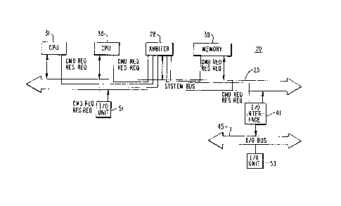
Fig, 1 shows an example of a data processing system
20 which embodies the present invention. The heart of system
20 is a system bus 25 which is a synchronous bus that allows
communication between several processors, memory subsystems,
and I/O systems. Communications over system bus 25 occur syn-
chronously using periodic bus cycles. A typical bus cycle time
for system bus 25 is 64 nsec.
In Fig. l, system bus 25 is coupled to two processors
31 and 35, a memory 39, one I/O interface 41 and one I/O unit
51. I/O unit 53, is coupled to system bus 25 by way of I/O bus
45 and I/O unit interface gl.
A central arbiter 28 is also connected to system bus
25 in the preferred embodiment of data processing system 20.
Arbiter 28 provides certain timing and bus arbitration signals
directly to the other devices on system bus 25 and shares some
signals with those devices,
13~1~.35~
--6--
The implementation shown in Fig. l is one which is
presently preferred and should not necessarily be interpreted
as limiting the present invention. For example, I/O unit 53
could be coupled directly to system bus 25, and arbiter 28 need
not operate in the manner described for the present invention.
In the nomenclature used to describe the present
invention, processors 31 and 33, memory 39, and I/O interface
41, and I/O device 51 are all called nodes. A "node" is
defined as a hardware device which connects to system bus 25.
According to the nomenclature used to describe the
present invention, the terms "signals" or "lines" are used in-
terchangeably to refer to the names of the physical wires. The
terms "data" or "levels" are used to refer to the values which
the signals or lines can assume.
Nodes perform transfers with other nodes over system
bus 25. A "transfer" is one or more contiguous cycles that
share a common transmitter and common arbitration. For exam-
ple, a read operation initiated by one node to obtain informa-
tion from another node on system bus 25 requires a command
transfer from the first to the second node followed by one or
more return data transfers from the second node to the first
node at some later time.
A "transaction" is defined as the complete logical
task being performed on system bus 25 and can include more than
one transfer. For example, a read operation consisting of a
command transfer followed later by one or more return data
transfers is one transaction. In the preferred embodiment of
system bus 25, the permissible transactions support the trans-
fer of different data lengths and include read, write (masked),
interlock read, unlock write, and interrupt operations. The
difference between an interlock read and a regular or
noninterlock read is that an interlock read to a specific loca-
tion retrieves information stored at that location and re-
stricts access to the stored information by subsequent
interlock read commands. Access restriction is performed by
setting a lock mechanism. A subse~uent unlock write command
stores information in the specified location and restores
`" 13~)~.3S~
access to the stored infor~ation by resetting the lock mecha-
nism at that location, Thus, the interlock read/unlock write
operations are a form of read-modify-write operation.
Since system bus 25 is a "pended" bus, it fosters
efficient use of bus resources by allowing other nodes to use
bus cycles which otherwise would have been wasted waiting for
responses. In a pended bus, after one node initiates a trans-
action, other nodes can have access to the bus before that
transaction is complete. Thus, the node initiating that trans-
action does not tie up the bus for the entire transaction time.
This contrasts with a non-pended bus in which the bus is tied
up for an entire transaction. For example in system bus 25,
after a node initiates a read transaction and makes a command
transfer, the node to which that command transfer is directed
may not be able to return the requested data immediately.
Cycles on bus 25 would then be available between the command
transfer and the return data transfer of the read transaction.
System bus 25 allows other nodes to use those cycles.
In using system bus 25, each of the nodes can assume
different roles in order to effect the ~ransfer of information.
One of those roles is a "commander" which is defined as a node
which has initiated a transaction currently in progress. For
example, in a write or read operation, the commander is the
node that requested the write or read operation; it is not nec-
essarily the node that sends or receives the data. In the pre-
ferred protocol for system bus 25, a node remains as the com-
mander throughout an entire transaction even though another
node may take ownership of the system bus 25 during certain
cycles o~ the transaction. For example, although one node has
control of system bus 25 during the transfer of data in re-
sponse to the command transfer of a read transaction, that one
node does not become the commander of the bus. Instead, this
node is called a "responder."
A responder responds to the commander. For example,
if a commander initiated a write operation to write data from
node A to node B, node 3 would be the responder. In addition,
in data processing system 20 a node can simultaneously be a
commander and a responder.
~ 3~ 3S6
Transmitters and receivers are roles which the nodes
assume in an individual transfer. A "transmitter" is defined
as a node which is the source of information placed on system
bus 25 during a transfer. A "receiver" is the complement of
the transmitter and is defined as the node which receives the
information placed on system bus 25 during a transfer. During
a read transaction, for example, a commander can first be a
transmitter during the command transfer and then a receiver
during the return data transfer.
When a node connected to system bus 25 desires to
become a transmitter on system bus 25, that node asserts one of
two request lines, CMD REQ (commander request) and RES REQ (re-
sponder request), which are connected between central arbiter
28 and that particular node. In general, a node uses its CMD
REQ line to request to become commander and initiate transac-
tions on system bus 25, arsd a node uses its RES REQ line to
become a responder to return data or message to a commander,
Generally, central arbiter 28 detects which nodes desire access
to the bus ti.e., which request lines are asserted). The arbi-
ter then responds to one of the asserted re~uest lines to grant
the corresponding node access to bus 25 according to a priority
algorithm. In the preferred embodiment, arbiter 28 maintains
two independent, circular queues: one for the commander re-
quests and one for the responder requests. Preferably, the re-
sponder requests have a higher priority than the commander re-
quests and are handled before the commander requests.
The commander request lines and responder request
lines are considered to be arbitration signals. As illustrated
in Fig. 1, arbitration signals also include point-to-point con-
ditional grant signals from central arbiter 28 to each node,
system bus extend signals to implement multi-bus cycle trans-
fers, and system bus suppression signals to control the
initiation of new bus transactions when, for example, a node
such as memory is momentarily unable to keep up with traffic on
the system bus.
Other types of signals which can constitute system
bus 25 include information transfer signals, respond signals,
~:30~.356
g
control signals, console/front panel signals, and a few miscel-
laneous signals. Information transEer signals include data
signals, function signals which represent the function being
performed on the system bus during a current cycle, identifier
signals identifying the commander, and parity signals. The re-
spond signals generally include acknowledge or confirmation
signals from a receiver to notify the transmitter of the status
of the data transfer.
Control signals include clock signals, warning sig-
nals, such as those identifying low line voltages or low DC
voltages, reset signals used during initialization, node fail-
ure signals, default signals used during idle bus cycles, and
error default signals. The console/front panel signals include
signals to transmit and receive serial data to a s~stem con-
sole, boot signals to control the behavior of a boot processor
during power-up, signals to enable modification of the erasable
PROM of processors on system bus 25, a signal to control a RUN
LIGHT on the front panel, and signals providing battery power
to clock logic on certain nodes. The miscellaneous signals, in
addition to spare signals, include identification signals which
allow each node to de~ine its identification code.
Fig. 2 shows an example of a node 60 connected to
system bus 25. Node 60 could be a processor, a memory, an I/O
unit or an I/O interface. In the example shown in Fig. 2, node
60 includes node specific logic 65, a node bus 57, and a system
bus interface 6~ containing a data interface 61 and a clock
decoder 63. Preferably, data interface 61, clock decoder 63,
and node bus 67 are standard elements for nodes connected to
system bus 25. The node specific logic 65, which uses differ-
ent integrated circuits from system bus interface 64, prefer~
ably includes, in addition to the circuitry designed by a user
to carry out the specific function of a node, standard cir-
cuitry to interface with the node bus 67. In general, data
interface 61 is the primary logical and electrical interface
between node 60 and system bus 25, clock decoder 63 provides
timing signals to node 60 based on centrally generated clock
signals, and node bus 67 provides a hiyh speed interface
between data interface 61 and node specific logic 65.
~3~.3~i6
-10-
In the preferred em~odiment of node 60 and system bus
interface 6~ shown in Fig. 2, clock decoder 63 contains control
circuitry for forming signals to be placed on system bus 25 and
processes clock signals received from central arbiter 28 to
obtain timing signals for node specific logic 65 and data
interface 61. Since the timing signals obtained by clock
decoder 63 use the centrally generated clock signals, node 60
will operate synchronously with syste~ bus 25.
Fig. 3 is a timing diagram showing one bus cycle, the
clock signals received by clock decoder 63, and certain of the
timing signals generated by clock decoder 63. The clock sig-
nals received by clock decoder 63 inclùde a Time H signal, a
Time L signal, and a Phase signal às shown in Fig. 3. Time H
and Time L are inverses of the fundamental clock signals and
the Phase signal is obtained by dividing the fundamental clock
signal by three. The timing signals generated by clock decoder q
63 include C12, C23, C3~, C45, CS6 and C61, all of which are
shown in Fig. 3. Those timing signals required by data inter-
face 61, which occur once per bus cycle, are provided to data
inter~ace 61, and a complete set of timing signals, including
equivalent ones of the timing signals provided to data inter-
face 61, is buffered and provided to the node specific logic
65. The purpose of buffering is to insure that node specific
logic 65 cannot adversely effect the operation of the system
bus interface 6~ by improperly loading the timing signals.
Clock 63 uses the cloclc signals to create six subcycles for
each bus cycle and then uses the subcycles to create the six
timing signals CXY, where X and Y represent two adjacent
subcycles which are combined to form one timing signal.
Each node in the sytem bus has its own corresponding
set of timing signals generated by its clock decoder 63. While
nominally the corresponding signals occur at exactly the same
time in every node throughout the system, variations between
clock decoder 63 and other circuitry in multiple nodes intro-
duce timing variations between corresponding signals. These
timing variations are commonly known as "clock skew."
5~
--11--
Fig. 4 shows a p~eferred embodimen~ of data interface
61. Data interface 61 contains both temporary storage cir-
cuitry and bus driver circuitry to provide a bidirectional and
high speed interface between each of the lines of node bus 67
and each of the lines of system bus 25. As shown in Fig. 4,
data interface 61 preferably includes storage elements 70 and
72 and system bus driver 7~ to provide a communication path
from node bus 67 to system bus 25. Data interface 61 also in-
cludes storage element 80 and node bus driver 82 to provide
communication path from sys~em bus 25 to node bus 67. As used
in the description of data interface 61, the term l'storage ele-
ment" refers generally to bistable storage devices such as
transparent latch or a master-slave storage element, and not to
a specific implementation. Persons of ordinary skill will rec-
ognize which types cf storage elements are appropriate.
As shown in Fig. ~, storage element 70 has an input
connected to receive data from node bus 67 and an output con-
nected to the input of storage element 72. The output of stor-
age e].ement 72 is connected to an input of system bus driver 74
whose output is connected to system bus 25. Storage elements
70 and 72 are controlled by node bus control signals 76 and 78,
respectively, which are derived from the timing signals gener-
ated by clock decoder 63. Storage elements 70 and 72 provide a
two-stage temporary storage for pipeLining data from node bus
67 to system bus 25. Different numbers of storage stages can
also b~ used.
System bus driver 74 is controlled by system bus
driver enable 79. According to the state of the system bus
driver enable 79, the input of system bus driver 7~ either is
coupled to its output, thereby transferring the data at the
output of storage element 72 to system bus 25, or decoupled
from that output. When system bus drive enable 79 decouples
the~input and output of the system bus driver 74, system bus
driver 7~ presents a high impedance to system bus 25. The sys-
tem bus drive enable 79 is also generated by clock decoder 63
in accordance with clock signals received from system bus 25
and control signals received from the node speciic logic 65.
5~
-12-
Storage element 80 has an input terminal connected to
system bus 25 and an output terminal connected to an input of
node bus.driver 82. The output of node bus driver 82 is con-
nected back to node bus 67. Storage element 80, preferably a
transparent latch, is controlled by a system bus control signal
85 which is deri~ed from the timing signals generated by clock
decoder 63. A node bus drive signal 87 contr-ols node bus driv-
er 82 similar to the manner in which system bus drive signal 79
controls system bus driver 7~. Thus, in response to node bus
driver signal 87, node bus driver 82 either couples its input
to its output or decouples its input from its output and pro-
vides a high impedance to node bus 67.
In order to explain how clata is transferred over sys-
tem bus 25, it is important to understand the relationship
between system bus drive enable 79 and control signal 85. In
the present embodiment, this relationship is shown in Fiy. 3.
System bus drive enable 79 is nominally driven from the begin-
ning to the end of a bus cycle. The new data become available
for receipt from system bus 25 at some time later in the bus
cycle after driver propagation and bus settling time has oc-
c~rred. In the present embodiment, storage element ao is a
transparent latch. Control signal ~5 is logically equivalent
to clock C45. The bus timing assures that system bus 25 data
is available for receipt sometime prior to the deassertion of
control signal 85. Storage element 80 stores bus data that is
stable at least a set-up time prior to the deassertion of con-
trol signal 85 and remains stable a hold time after the
deassertion of control signal 85.
Node bus 67 is preferably a very high speed data bus
which allows bidirectional data transfer between the node spe-
cific logic 65 and system bus 25 by way of data interface 61.
In the preferred embodiment of node 60 shown in Fig. 2, node
bus 67 is an interconnect system consisting of point-to-point
connections between the system bus interface 64 and the node
specific logic 65. In accordance with the present invention,
however, there is no requirement for such point-to-point inter-
connection,
~3~ 56
--13--
F;g. 5 shows a preferred embodiment of the central
arbiter 28 which is also connected to system bus 25. Central
arbiter 28 provides the clock signals for system bus 25 and
grants ownership of the bus to the nodes on system bus 25.
~entral arbiter 28 preferably includes an arbitration circuit
90, a clock circuit 95, and a oscillator 97. Oscillator 97
generates the fundamental clock signals. Clock 95 provides
timing signals for arbitration circuit 71 and the basic Time H,
Time L, and Phase clock signals for timing on system bus 25.
Arbitration circuit 71 receives the commander and responder re-
quest signals, arbitrates conflicts between nodes desiring
access to system bus 25, and maintains the queues referred to
above for the commander and responder requests. Arbitration
circuit 71 also provides certain control signals to clock 95.
B. Discussion of In~erlock_Operations
As briefly discussed above, a number of different
types of transactions are allowed on bus 25. In each case, the
transaction is composed of one or more separate transfers from
one node to another. When the responder node successfully re-
ceives a command transfer during one or more bus cycles, it
generates an acknowledge confirmation at the beginning of the
s~cond bus cycle after each cycle of the transfer. Such
acknowledgement signals do not indicate successful execution of
the command contained in the original transfer, but merely in-
dicate that the transfer was successfully placed in an input
queue in the desired responder node. The transactions relevant
to the present invention will be briefly described below.
A read transaction is used to move data in four-byte,
eight-byte, sixteen-byte, or thirty two-byte blocks from a spe-
cific location in a responder node managing a region of address
space to a commander node. In the preferred embodiment, memory
and I/O operations are referenced to a common address space. A
responder node can be either a memory node, a processor node,
or an I/O node.
Interlock read transactions are similar to read
transactions. However, the exact effect of an interlock read
transaction depends on the state of lock tags in the responder
~.3~ ;6
-14-
node. Lock tags prevent access to locations or groups of loca-
tions in address space. The effect of lock tags can be under-
stood by visualizing address space of system 20 as appearing
across a metallic "blackboard." Lock tags operate like magnet-
ic tags removeably placed on top o~ locations or groups of lo-
cations on the address space "blackboard." If the location in
address space specified in an interlock read transaction is
already covered with a lock tag, that is, if the specified
address space is "locked," the responder node responds to the
interlock read request with a "locked" response message and no
data is returned. This signifies to the commander that the lo-
cation in address space specified in the interlock read command
is not accessible. This locked response message is transmitted
to the commander after the responder node services the
int-erlock read command and after the responder node can gain
access to bus 25. Thus, the commander receives the locked re-
sponse message at an unspecified time after the command trans-
fer of the interlock read transaction.
If the specified location is not loclced, that is, not
associated with a lock tag, information stored in the address
specified in the interlock read command is returned in a re-
sponse message to the commander node which generated the
interlock read command. The responder node also attaches a
lock tag to the location in address space specified in the
interlock read command, thus denying access to the specified
location in address space to subsequent interlock read
commands.
The unlock write transaction is the complement to the
interlock read transaction. When a commander node successfully
completes the read and modify location in a read-modify-write
operation, it must ~nlock the location in address space which
it temporarily locked by an interlock read command. The com-
mander accomplishes this operation by performing an unlock
write transaction to the specified location in address space to
write the appropriately modified data into the specified loca-
tion. The responder node processes the unlock write command by
unlocking the address space and writing the data as requested.
The lock tag is then cleared.
1 356
-15-
The message transmitted over bus 25 during an
interlock read command transfer includes data on sixty four
data lines. That data contains a four-bit command field, a
two-bit length field which specifies the number of words to be
transferred from e.g., memory 39 to processor node 31, and a
thirty-bit address field which specifies the address location
in memory 39 from which data is desired to be read. Other
lines of system bus 25 carrying information during an interlock
read command include four function lines carrying a four-bit
function code indicating a command transfer, six ID lines
carrying a six-bit code identifying the commander node which
initiated the interlock read command, and three parity lines.
As briefly discussed above, system bus 25 includes
respond signals which are used by a receiver to indicate suc-
cess~ul reception of information placed on the bus by a trans-
mitter. In the preferred embodiment, the respond signals in-
clude three identical wire-ORed confirmation (CNF) lines.
Three lines are provided since it is extremely important to the
integrity of bus transactions that a commander know exactly
what a responder has done in response to each command, particu-
larly in the case of an interlock command or a write to an I/O
register. Therefore, a receiver will send either a acknowledge
(ACK) confirmation by asserting all three CNF lines or a no
acknowledge (NACK) confirmation by not asserting all three CNF
lines. Error correction logic is provided in the receiver to
determine the true CNF status if all three CNF lines are not
received by the receiver at the same logic level.
An ACK confirmation indicates that a responder has
accepted information from one cycle of command transfer or that
a commander has accepted information from one cycle of a re-
sponse message. A read command transfer cycle resulting in an
ACK confirmation indication indicates that the responder will
return a read response message at some later time.
A NACK confirmation returned on the CNF lines indi-
cates that no receiver has accepted the information from that
bus cycle of the command transfer. This could be for three
reasons: (1) a parity error has occurred on the system bus 25,
13~ 3~;~
-16-
(2) the receiver was temporarily unable to accept the command,
for example, when the receiver's input queue is full, or (3)
there is no responder node corresponding to the specified
address.
The confirmation indications corresponding to a bus
cycle are placed on the CNF 1 ines by the receiver node at the
beginning of the second cycle after cycle of the bus cycle.
An example of an interlock read transaction will be
described in connection with Figure 6. The horizontal axis at
the top of Figure 6 indicates successive bus cycles on bus 25.
The labels appearing vertically along the left side of Figure 6
indicate groups of lines contained in bus 25, that is, function
lines, data lines, ID lines, confirmation lines, and arbitra-
tion lines. The entries in the matrix formed by the horizontal
and vertical axes of Figure 6 describe the type of data
appearing on the specified bus lines during the specified bus
cycles.
At bus cycle 0, a first commander node, for example,
node 31 of Figure 1, asserts its CMD REQ arbitration request
line (one of the point to point lines connected to arbiter 28
and shown in Fig. 1) to arbiter 28. Figure 6 thus indicates a
"cmdr #l" request present 011 arbitration lines of system bus 25
at cycle 1. Assuming that no other node of higher priority is
simultaneously requesting access to the bus, processor 31
obtains bus access on cycle 1 and transmits a message into sys-
tem bus 25.
~ uring cycle 1 information placed on the function
lines of bus 25 indicates that the information on the bus is
command (cmd) information. The data placed on data lines of
bus 25 consist of comnland and address (c/a) data identifying
the current transaction as an interlock read transaction and
specifying the address in memory 39 from which data is to be
returned to processor 31. The ID lines during bus cycle 1 con-
tain the identification code of processor (commander/cmdr) node
31 currently transmitting on bus 25.
During bus cycle 2, no information is ?laced on
bus 25 in connection with the present interlock read
transaction.
~3~ 56
--17--
At the beginning of bus cycle 3, which is two cycles
(i.e., a predetermined time) after initiation of the interlock
read transaction, ~emory node 39 transmits an ACK confirmation
on the confirmation lines of bus 25 if memory 39 successfully
received the command transfer transmitted during bus cycle 1.
Memory 39 then places the commancl message in the input queue of
memory 39,
The end of bus cycle 3 constitutes the end of the
first ~ransfer in the interlock read transaction. Due to the
pended nature of transactions on bus 25, the time when the re-
quested information will be returned from memory 39 to
processor 31 is not precisely defined. The response time
depends on the length of time required by memory 39 to process
the request and the amount of time necessary for system bus 25
to handle additional traffic on bus 25 generated by other
nodes. The unspecified nature of the time between the two
transfers of an interlock read transaction is indicated by the
dotted line in Figure 6 between bus cycles 3 and 4. Thus,
although subsequent information is indicated by Figure 6 to
occur over bus cycles 4 through 7, it is to be understood that
this is only a specific example of the timing involved in an
interlock read transaction and that the second transfer of such
transaction could occur in any subsequent cycle of bus 25.
Memory 39 processes the interlock read command by re-
moving the interlock read transfer message from its input queue
in turn and examining the address information contained in the
transfer, The information is compared to address values stored
in lock tags to be more completely described. If there is a
match between the stored address values and the address infor-
mation of the interlock read transfer, this is an indication
that the desired address location has been locked by a previous
interlock read command. Memory 39 then generates a locked re-
~ponse message including a "locked" function code, along with
other information required for a response message, in an output
queue of memory node 39.
If the comparison of address values stored in lock
tags with the interlock read transfer address information does
~3~ 5~
-18-
not yield a "hit," that is, if the transferred address does not
correspond to any stored address, memory node 39 constructs a
response message consisting of a valid read response node such
as "good read data" (~rdO) code for functions lines, the con-
tents of the specified address location for the data lines, and
the commander identification code of the commander node which
initiated the interlock read command for the ID lines. This
response message is loaded into the output queue of memory node
39.
When memory 39 has processed the interlock read
transaction and generated a response message within its output
queue in a manner to be more completely described, memory 39
asserts its RES REQ request line (another point-to-point line
shown in Fig. 1) to arbiter 28. The arbitration lines thus
carry a responder request (resp) indication as shown in Figure
6 at bus cycle 4. Assuming that no other nodes have higher
priority at this time, arbiter 28 grants memory 39 access to
bus 25 during bus cycle 5. Memory 39 transmits the response
message including "good read data" (grdO) signal onto function
lines of system bus 25, eight bytes (i.e. 64 bits) of data over
the data lines of system bus 25 from the memory locations
specified by the address field of the initial transfer from
processor 31 to memory 39, and the ID of processor 31 onto the
ID lines of bus 25 to associate the returning data with the
commander (i.e. processor 31) which initially issued the
interlock read request.
During bus cycle 6, no traffic appears on system bus
25 related to this interlock read transaction. Finally, the
interlock read transaction concludes in bus cycle 7 when
processor 31 transmits an ACK confirmation onto the confirma-
tion lines of bus 25.
A second interlock read transaction to the same
specified location in memory will result in data appearing on
bus 25 as shown in cycles 8-15 of Fig. 6. At cycle 8, a second
commander (cmdr #2) initiates a commander request to arbitor
28. Bus cycles 9-12 result in traffic on bus 25 identical to
cycles 1-4. However, memory 39, upon processing of the
-
~3~ S~
--19--
received interlock read command, found a match between the
address values stored in lock tags and the address transmitted
with the interlock read command. Accordingly, a LOC response
is presented on function lines of bus 25 at, for example, cycle
13. Bus cycles 14 and 15 are identical to cycles 6 and 7.
C. Description of Processor 31
Referring now to Figure 7, there is shown a more
detailed block diagram of certain elements of the node specific
logic 65 in processor 31. Processor node 31 includes, as do
all the nodes, bus interface circuit 6~. Processor node 31
also includes a processor logic 202. As shown in Fig. 7, pro-
cessor logic 202 includes central processing unit (CPU) cir-
cuitry required to execute software in a manner well known to
those skilled in the art. Processor logic 202 also generates
command and address information as required by system 20 to
execute the necessary application functions as well as to con-
tr~l transfers over system bus 25.
Processor node 31 also includes a parity error check
circuit 204 which monitors information on the function, data,
ID, and parity lines of system bus 25 received from bus inter-
face circuit 64 to perform a parity check on those signals in a
manner well known in the art. A detected parity error will
result in the generation of a parity error indication on signal
line 206.
The information on the ID lines is monitored by a
comparator circuit 208 which is also supplied with the identi-
fication code of processor 31 from a hard-wired connection 210
on the backplane which is determined by the position of proces-
sor 31 in a mounting cabinet. The comparison result from
comparator 207 is supplied, along with information on the pari-
ty error signal line 206, to an acknowledge confirmation gener-
ator 20~. If no parity error was detected and if the ID code
received over bus 25 for a response message matches the ID code
of processor 31, ACK indications are transmitted over the CNF
lines of bus 25 by an acknowledge indication generator 208 at
the beginning of the second bus cycle af ter each cycle of a re-
sponse transfer directed to processor 31.
~301 35~i
-20-
Information on function and data lines of bus 25 is
supplied through bus interface 64 to a response decoder 212.
Decoder 212 is enabled by comparator 207 when a message over
bus 25 is intended for processor 31. This is determined by a
positive comparison result from comparator 207. If decoder 212
is enabled by comparator 207, decoder 212 extracts function
codes from function lines of system bus 25, and for certain
function codes, supplies command and data information from data
lines of bus 25 to processor logic 202 for appropriate action.
In accordance with the present invention, the proces-
sor includes means responsive to a resource denial indication
for asserting a lockout activator when access commands from the
processor receive inadequate response from a resource node
according to predetermined lockout assertion criterion. As
embodied herein, such means comprises a denial detector circuit
213. Lock detector 213 is responsive to function information
derived by response decoder 212 from the function lines of bus
25 to assert lockout activator 215 when a locked response code
is received in a response message from memory 39 (Fig. 1) as
decoded by decoder 212. The lockout activator 215 is supplied
to a driver 255 such that when lockout activator 215 is
asserted, processor 31 asserts lockout indicator 240.
In accordance with the present invention, the proces-
sor also includes means for transmitting access commands over
the bus to memory. As embodied herein, the transmitting means
comprises a command generator 214. When processor 31 desires
to initiate a transaction on bus 25, cornmand, address, and data
information is supplied to command generator 214, along with
the ID of processor 31 supplied from connection 210. Command
generator 214 prepares a command message and asserts the com-
mander request (CMD REQ) arbitration line 216 for processor 31.
A line 216g, which is a gated version of CMD REQ line 216
con~itioned by lockout check circuit 250 to be described in
greater detail hereinafter, indicates to arbiter 28 (not shown
in Fig. 7) that processor 31 desires access to bus 25 to trans-
mit a commander message. Using an arbitration system, arbiter
28 grants bus access to processor 31 at an unspecified time
after the original interlock read transfer.
~3q~ 56
-21-
Upon being granted access, command generator 214
causes bus interface 6~ to transmit the command message from
command generator 214 to system bus 25.
The responder node to which the interlock read
command is directed will generate an acknowledge confirmation
two cycles after the interlock read command transfer. As shown
in Fig. 7, command generator monitors CNF lines to detect the
presence of an ACK confirmation on the CNF bus lines two bus
cycles after a command transfer transmitted by a processor 31
over system bus 25. Failure to detect the presence of an ACK
confirmation will result in appropriate corrective action
which, in the preferred embodiment, consists of the
retransmission of the previous command. When the transfer is
complete, the responder node will process the interlock read
command and return a response message on system bus 25.
Lecause of uncertainties due to traffic on system bus 25 and
queue lengths, the responder node will generate a response mes-
sage at an unspecified time after the command transfer.
System 20 inc].udes a lockout indicator 240 which in-
cludes a wired-OR line. Lockout indicator 240 is operable when
asserted to limit the generation of interlock read commands by
processors on system 31. In the preferred embodiment, lockout
indicator 240 is connected to all nodes. However, the inven-
tion does not require that lockout indicator 2~0 be connected
to all nodes.
In accordance with the present invention, the proces-
sor includes lockout check means for monitoring the lockout in-
dicator and for preventing generation of access commands by the
processor according to a predetermined access gating criteria
when the lockout indicator is in an asserted condition. As
embodied herein, the lockout check means comprises a lockout
check circuit 250. Lockout check circuit 250 receives a grant
signal 252 which is a line from bus interface 64 which is
asserted at the time processor 31 is granted access to bus 25.
Lockout check circuit 250 also receives an interlock read
command indication 25~ from processor logic 202, lockout
activator 215 from lockout detector 213, and a signal from
~L30~ ~56
-22-
lockout indicator 240. Lockout check circuit 250 monitors the
statùs of lockout indicator 2~0 such that under certain condi-
tions when lockout indicator 2~0 is asserted, lockout check
circuit 250 suppresses the generation of CMD REQ level on line
216g to arbiter 28 to prevent processor 31 from generating an
interlock read transfer.
In an alternative embodiment, the lockout check means
may be incorporated in a state machine formed by a programmable
logic array.
D. Description of MemorY 39
Fig. 8 shows a block diagram of memory 39 which may
function as a responder node. As can be seen in Fig. 8, memory
39 includes a command decode and address and parity check cir-
cuit 300. Circuit 300 is connected to the bus function,
address, and identifier lines and performs a parity check in a
well-known manner. Circuit 300 also compares the information
on bus address lines to the limits of address space served by
memory 39, as supplied from a register 302, and supplies the
results of this comparison on an address match line 301. If
the address inforrnation rece;ved over bus 25 is within the
range of address space served by memory 39 and if no parity
error has occurred, an acknowledge generator 304, connected to
circuit 300, will generate an ACK confirmation by asserting all
three CNF lines at the beginning of the second cycle after the
transmission cycle of a transfer destined for memory 39.
Memory 39 includes an input queue 306 for storing
messages tconsisting of function, ID, and data information) re-
ceived from transfers over bus 25, ~ia bus interface unit 64.
Input queue 306 permits such messages, received at high speed
over bus 25, to be stored until the relatively slower logic of
memory 39 allows such messages to be acted upon. Input queue
306 is enabled to store a message from bus 25 when address in-
formation appearing in the data field of a message on bus 25 is
within the limits of address space for memory 39, as determined
by the level on address match signal 301.
The output of input queue 306 is supplied to a
decoder 308 which extracts address and command information from
~3~)~13~i6
23 66822-51
messages stored in input queue 306. ~lthough decoder 308
supplies multiple indications to decode the various commands
and provides address information on a set of parallel signal
lines, the address and command oukputs of decoder 306 are
respectively shown in Fig. 8 as bundled lines 309 and 311 for
purposes of clarity.
In a~cordance with the invention, the memory
comprises means responsive to access commands from the
processor. As embodied herein, such means comprises a lock
controller 310 and a memory array 312. Lock controller 310 is
described more completely in the aforementioned U.S. Patent
4,858,116. The address and command information is supplied to
lock controller 310 which assis~s in processing interlock read
and unlock write commands. Address and command information
from decoder 308 is also supplied to memory array 312. Memory
array 312 responds to read and write commands to read data from
and ~rite data to locations in array 312 speci~ied by address
information received from decoder 308. As is well known in the
art, information is stored in memory array 312 in a plurality
of discrete locations identified by addresses whlch may be
spe~ified by read and write commands supplied to the array 312.
Lock status signal 314 from controller 310 and memory
data from memory array 312 are supplied to a response genera~or
316 which generates an output response message. Response
messages from generator 312 are supplied to an output ~ueue 318
for storage until memory 39 obtains access to the bus through
the arbitration process described previously.
Memory 3~ includes a response generator 316 and an
output ~ueue 318. Response generator 316 prepares a response
message based on data received from memory 312, the level of
lock s~atus signal 314 received from controller 310, and
command and ID information received from decoder 308. The
A
356
- 23a - 66822-51
response message prepared by generator 316 is either of two
typesr depending on whether memory 39 is permitted to supply
the reques~ed data. If the command being responded to is a
YA
~.3~ 56
-2~-
non-interlock read command, or if the command is an interlock
read command and lock status signal 314 is not asserted, re-
sponse generator 316 prepares a first type of message including
the requested contents of the specified location in memory 312.
However, if the command is an interlock read command and the
lock status line 314 is asserted, response generator 316 pre-
pares the second type of message with a "locked" code for the
function lines indicating that the specified address of the
interlock read command was in a locked condition and that the
requested data is therefore not provided in the response mes-
sage transmitted by memory 39 in response to the received
interlock read command.
When generator 316 has compiled the response message,
it is supplied to output queue 318. Output queue 318 alerts
bus interface 64 that memory 39 desires access to bus 25. The
response message is stored in output queue 318 for an
unspecified time until such access is obtained.
When memory 39 is granted access to bus 25, the re-
sponse message contained in output queue 318 is placed on sys-
tem bus 25 for transmission to the commander node which ori~i-
nally generated the command. Since it is not known at what
time memory 33 will complete the execution of the command orig-
inally transmitted by the commander node and since it is fur-
ther uncertain at what time memory 39 will obtain access to bus
25 to provide either the requested data or the lock status in-
formation, the lock status information corresponding to the
interlock read command will appear on the function lines of bus
25 at the commander node at an unspecified time subsequent to
initiation of the original interlock read command.
E. Description of Lockout Check Circuit 250
and Lock Detector 213
. . . _ _ . . . _ . _
In accordance with the invention, lockout check means
are included for monitoring the lockout indicator and for pre-
venting generation of access commands by the processor to memo-
ry according to predetermined access gating criteria when the
lockout indicator is in the asserted condition. As embodied
herein, the lockout check means comprises lockout check circuit
~3QI~3~i
250. Preferably, the processor further includes means respon-
sive to a resource denial indication for asserting a lockout
activator when access commands from the processor have received
inadequate response by the memory according to a predetermined
lockout assertion criterion. As embodied herein, such
asserting means comprises denial detector circuit 213 respon-
sive to a resource denial indication which, in the preferred
embodiment, comprises a locked response. Fig. 9 shows a block
diagram of denial detector circuit 213 and lockout check cir-
cuit 250.
Decoder 212 supplies control lines 402 and 404 re-
spectively indicating the presence of a locked response or a
valid read data response. Locked response signal 40~ is
supplied to the set terminal of denial circuit 213 which in the
preferred embodiment is a set-reset a storage element, the
reset terminal of which is connected to valid read data re-
sponse si~nal 404. The output of storage element 213 consti-
tutes lockout activator 215 which is supplied to driver 255
such that lockout indicator 240 is asserted by denial detector
circuit 213 whenever a locked response is received by processor
~1 over bus~25.
The receip~ of a single locked response by processor
31 constitutes a predetermined lockout assertion criterion.
That is, a single locked response is interpreted by processor
31 as an indication that processor 31 is not achieving or main-
tainin~ adequate access to memory 39. It is to be understood
that invention is not limited to the specific lockout assertion
criterion employed in the preferred embodiment, but that other
criteria may be employed. For exarnple, a counter could be used
in place of storage element 213 such that lockout indicator 2~0
would only be set when processor 31 receives a plurality of
locked responses, for example, three locked responses. Alter-
natively, a timer could be provided as a denial detector cir-
cuit.
Lockout activator 21S is also connected to lockout
check circuit 250. Lockout check circuit 250 includes a
three-input ~ND gate 408. The first input to AND gate 408 is
~3~ 56
-26-
lockout indicator 240. The second input to AND gate 408 is the
inverted level of lockout activator 215. The third input to
AND gate ~08 is interlock read line 254 from processor logic
202, the assertion of which indicates that an interlock read
transaction is currently beinq requested by processor logic
202-.
The output of AND gate 408 constitutes a "suppress"
indicator which is supplied in inverted form to a two-input AND
gate 410. The other input of AND gate 410 is CMD REQ (com-
mander request) line 216 from command generator 21~. The out-
put of AND gate 410 is supplied to the set terminal of a stor-
age element 414. ~he reset terminal of storage element 414 is
supplied by grant signal 252 supplied from bus interface 64
(Fig. 7) which, when asserted, indicates that procesor 31 has
access to bus 25.
Denial detector 213 and lockout check circuit 25Q,
along with lockout indicator 240 provide a method and apparatus
for assuring adequate access to memory 39 by processor nodes
including node 31. When a locked response is rece;ved from
memory 39 by processor 31 in response to an interlock read
command, this is an indication that processor 31 has been
denied access to a portion of memory 39. ~y setting lockout
indicator 240, processor 31 can cause other processing nodes to
restrict their generation of new lockout read commands. Spe-
cifically, upon receipt of a locked response by processor 31
and the subsequent assertion of lockout indicator 240, no pro-
cessor node connected to lockout indicator 240 which had not
already requested bus access for an interlock read command
prior to assertion of lockout indicator 240 will be permitted
to generate a new interlock read command. This is accomplished
by the suppression of the CMD REQ line by AND gate 408. This
suppressiQn takes place if the following conditions,
constituting predetermined access gating criteria of the pre-
ferred embodiment, are present: an interlock read operation is
being requested by the processor (i.e., line 254 is being
asserted), (2) the lockout activator 215 for this node is not
currently asserted, and (3) lockout indicator 240 is asserted.
~La~ L 356
-27-
Other access gating criteria could of course be pro-
vi-ded. For example, suppression of the CMD REQ line could be
conditional on the failure of proc:essor 31 to acquire a valid
read data response for more than a predetermined time.
It is not necessary that denial detector circuit 213
and lockout circuit 250 both be present in lock commander node.
That is, it may be desired to provide a commander node which
sets lockout indicator 240 but does not to prevent generation
of access commands or access denial commands.
An example of the operation of the preferred embodi-
ment o~ the present invention on a multiple node system ;s
shown in Fig. 11. Fig. 11 illustrates characteristics of four
processor nodes on a system similar to system 20, specifically,
nodes 15, 7, 6, and 2, as the nodes implement read-modify write
operations using an interlock sequence consisting of a success-
ful interlock read transaction and an unlock write transaction.
The far left column indicates an arbitrary transaction number
on bus 25. Th~ next three columns at the left of Fig. 11 re-
spectively show the node which is the commander during this
transaction, the type of command information being placed on
the bus by that node, and the response message returned by mem-
ory 39 in response to the node command. The next column of
Fig, 11 indicates those nodes which are asserting lockout indi-
cator 2~0 at a given point in time. The columns numbered 15,
7, 6, and 2 indicate the status of the respective nodes 15, 7,
6, and 2 at the end of each time. The numbering of nodes in
Fig. 11 refers to their physical position in a cabinet and not
to re~erence characters in the drawings.
Prior to the start of transaction #l shown in Fig,
11, that is, the top row of Fig. 11, nodes 15, 7, and 6 are all
in the interlock read transaction generation state. That is,
each of these nodes is attempting to gain access to the same
location in memory 39. Node 2 is in the idle state.
In transaction #1, node 15 obtains access to bus 25
and places an interlock read request on the bus. ~ince node 15
is the first to gain access to the specified location in memory
39, such location is unlocked and memory 39 returns a valid
56
-28-
read data (GRD) response on function lines of bus 25.- No nodes
are asserting lockout indicator 240 at that time. Since node
15 has received a valid read data response, it advances to the
unlock write generation state. Nodes 7, and 6 remain in the
interlock read transaction generation state.
In transaction #2, of Fig. 11, node 7 obtains access
to the bus and initiates an interlock read transaction to the
same memory location. Since node 15 had previously accessed
that location and caused memory 39 to lock the location, memory
39 returns a locked (LOC) response message on function lines of
bùs 25. Since node 7 has now received a locked response, node
7 asserts lockout indicator 240 as shown in the third row of
Fig. 11. Nodes 7 and 6 remain in the interlock read transac
tion generation state. Node 2 remains in the idle state.
At transaction ~3, node 6 obtains access to the bus
and initiates an interlock read transaction to the same loca-
tion in memory 39. Since this location is still locked by vir-
tue of the first interlock read operation of node 15, node 6
receives a lockecl response on function lines of bus 25. Node 6
also asserts lockout indicator 240. At this time, both nodes 7
and 6 are asserting lockout indicator 240. Node 15 remains in
the unlocked write generation state, since it is not yet been
able to obtain access to bus 25. Similarly, nodes 7 and 6 re-
main in the interlock read transaction generation state since
they have not been able to successfully complete an interlock
read transaction.
At transaction #4, node 15 obtains access to the bus
and performs an ùnlock write transaction, thereby completing
this interlock sequence. As shown in Fig. ll, no response mes-
sage is required. Since nodes 7 and 6 both have unsuccessful
interlock read requests pending, nodes 7 and 6 continue to
assert lockout indicator 240. Node 15 returns to the idle
state and nodes 7 and 6 remain in the interlock read generation
state. At transaction #4, it is assumed that node 2 has
decided to initiate an interlock read transaction. However,
since such operation was not initiated prior to assertion of
lockout indicator 240 by node 7, node 2 does not enter the
56
-29-
transaction generation state, but enters the interlock read
wait state (IRW)
At transaction #5, node 7 obtains access to the bus
and initiates an interlock read transaction. Since the
specified location in memory has been unlocked by the previous
unlocked write transaction of node 15, node 7 is able to obtain
access to the information contained in the specified memory lo-
cation and memory 39 provides a valid read data response mes-
sage on the function lines of bus 25. Since node 7 has suc-
cessfully obtained its data, it no longer asserts lockout
indicator 240 and it moves to the unlock write state~ The suc-
cessful interlock read transaction of node 7 causes memory 39
to set the lock bit of the specified location and memory. Node
6 continues to assert lockout indicator 240. Node 15 remains
in the idle state. Node 6 remains in the interlock read gener-
ation state and node 2 remains in the interlock read wait
state.
At transaction #6, node 6 obtains access to bus 25
and initiates an interlock read transaction. However, the
speci~ied location in memory is loc:ked due to the immediately
preceeding interlock read transaction of node 7. Thus, memory
39 returns a locked response to nocle 6 on the function lines of
bus 25. Accordingly, node 6 continues to assert lockout indi-
cator 240. At this time, node 15 has decided to attempt to in-
itiate another interlock read transaction. However, since the
initiation of this transaction did not take place prior to the
assertion of lockout indicator 2~0, node 15 is placed in the
interlock read wait state. Node 7, having completed the "read"
and "modify" portions of the read-modify~write operation, is
now in the unlock write generation state. Node 6 remains in
the interlock read generation state and node 2 remains in the
interlock read wait state.
At transaction #7, node 7 obtains access to bus 25
and performs an unlock write transaction, thereby completing
this interlock sequence. No response message is returned.
Since node 6 still has not successfully completed an interlock
read transaction, node 6 continues to assert lockout indicator
56
-30-
2~0. Node 15 remains in the interlock read wait state, and
node 7, having successfully completed all phases of the
read-modify-write operation enters the idle state. Node 6 re-
mains in the interlock read genez-ation state and node 2 remains
in the interlock read wait state. The lock bit of the
specified location in memory 39 is reset.
At transaction #8 of Fig. 11, node 6 obtains access
to bus 25 and initiates an interlock read transaction. Since
the specified location in memory is now unlocked, due to the
unlock write transaction of node 7 in the previous transaction,
node 6 is successful in obtaining access to the specified loca-
tion and memory 39 returns a valid read data response message.
Since all nodes which have been attempting interlock read
transactions have now successfully completed such transactions,
no nodes are asserting lockout indicator 240. Nodes 15 and 2
can thus transition from the interlock read wait state to the
interlock read generation state. Node 6 then enters the unlock
write generation state.
At transaction #11 of Fig. 9, node 6 obtains access
to bus 25 and performs an unlock write transaction and returns
to the idle state. No response message is returned. Since no
nodes have received a locked response, no nodes are currently
asserting lockout indicator 240. Nodes 15, 7, and 2 all remain
in the same state as the previous transaction.
Although the present invention has been described in
detail with respect to interlock read/unlock write transactions
and in which a memory node returns a resource denial indication
due to interlock operations, the invention is not so limited.
Rather, the invention may be applied to assure adequate access
to other types of resources. For example, the invention may be
applied to assure adequate access to the input queue of a memo-
ry node. Since a "no acknowledge" indication is returned to a
processor node whose access command to memory was refused due
to the memory input queue being full, such "no acknowledge"
messaqe constitutes a resource denial indication. Lockout in-
dicator 240 can thus be used in combination with a lockout
check means and means for transmitting and receiving "no
-` ~3~ i6
-31-
acknowledge" indications, such that processor nodes can be in-
hibited, under appropriate conditions, from generating further
access comrnands which would require processing by an input
queue in memory. Thus, the demands on the memory can be re-
duced until such time as the memory node is able to reduce the
backlog in its input queue.
In the same manner as discussed in detail above with
respect to the interlock read unlock/write operations, the
present invention can thus assure adequate access to the memory
node input ~ueue resource by all nodes. Similarly, adequate
access to an input queue in adapter 41 (~ig. 1) can be assured
using the principles of the present invention. Also, the
invention can be applied to assure adequate access to con-
trol/status registers in nodes such as I/O controllers and pro-
cessors.
It will be apparent to those skilled in the art that
various modifications and variations can be made in the appara-
tus and methods of this invention without departing from the
spirit or scope of the present invention. The present inven-
tion covers such modifications and variations which are within
the scope of ~he appended claims and their equivalents.