Note : Les descriptions sont présentées dans la langue officielle dans laquelle elles ont été soumises.
~30i8~
97-577-2
118/
TITLE OF T~E INVENTION
.
AUTOMOTIVE IGNITION SYSTEMS
BACKGROUND OF T~E INVENTIOM
Field of the Invention
This invention relates generally to automotive
ignition systems, and more specifically to a multi-
strike ignition system which produces a train of
ignition sparks at the spark gaps of an internal
combustion engine in proper timed sequence during a
demanded firing duration, which is defined as the
lapsed time during which multisparks ~7ill occur at the
spark plug.
Description of the Prior Art
(~ A conventional multi-strike ignition system is
disclosed in the United States Patent 3,489,129,
wherein a charge circuit for charging a ignition
capacitor from a DC voltage converter includes a
resistor and a first thyristor used as a charge
switch. A discharge circuit, for discharging the
ignition capacitor to a primary winding of a ignition
transformer, has a second thyristor used as a discharge
switch. After the first tnyristor is turned on, a
~30la~4
--2--
charge current flows to the ignition capacitor from the
DC voltage converter via the resistor and the first
thyristor for a period of time determined by the time
constant of the combination of the ignition capacitor
and the resistor. As the result, the first thyristor
operated as the charge switch canno~ be turned off
until the current flo~ing through the first thyristor
is reduced due to thç characteristic of the
thyristor. The conditions necessary to turn off the
thyristor include whether the current flowing through
the thyristor is very small or whether a reverse
voltage is applied to the thyristor. Therefore, the
interval for charging the ignition capacitor is much
longer and hence a timing for discharging the ignition
capacitor to the primary winding of the ignition
transformer is delayed whereby the duty cycle of the
multi-strike spark is reduced.
Furthermore, in the conventional ignition system,
a timed sequence control for operating the charge
circuit of the ignition capacitor and the discharge
circuit of the ignition capacitor is operated by an
oscillator which oscillates with a predetermined
frequency without regard to the states of the
thyristors.
Therefore, if the first thyristor is operated as a
charge switch it may to be turned on by the oscillator
`` 130~8Z4
--3--
in spite of the turned on state of the second thyristor
which is being operated as the discharge switch. This
is due to the turned on period of the second thyristor
when misfiring occurred at the spark plug. The primary
winding of the ignition transformer is directly loaded
with the DC volta~e frorn the DC voltage converter,
whereby the DC voltage converter is fully discharged.
Subsequently, the recovery time of the DC voltage
converter, to return to the predetermined firing
voltage is much longer and, therefore, the spark plug
cannot be fired during this recovery time.
In the conventional multi-strike ignition system,
the firing duration is fixed to a predetermined value
and is independent of the rotational speed of the
engine. In order to stabilize engine combustion and
reduce the consumption of electrical energy, a firing
duration control, in response to the rotational speed,
is required. ~'or example, the firing duration may be
increased in response to the decrease in the rotational
speed of the engine because the compressed fuel air
mixture within the combustion chamber of the engine is
less combustible at low speed conditions due to a low
mixture swirl speed or low temperature of the
cornbustion chamber. Conversely the firing duration may
be made to decrease in response to the increasing of
the rotational speed of the engine because the
~30~82~
compressed fuel-air mixture within the combustion
chamber of engine is more combustible at high speed
condition o~ engine due to the high temperature in the
combustion chamber.
Additionally, in the conventional multi-strike
ignition system, and especially the multi-strike
ignition system using the ignition ca2acitor, the
ignition transformer is a high leakage inductance type
transformer having a air gap. The type of transformer
which has an air gap is generally used in an inductive
discharge ignition system which stores the spark energy
; in the form of magnetic energy in the air gap. This
particular type of transformer is often used as a part
fo a capacitive discharge ignition system having the
above described ignition capacitor. The transEormer is
used because of the economic considerations.
d The air gap is necessary in order to provide
storage of energy in the inductive discharge ignition
system. On the other hand in capacitive discharge
ignition systems which utilize the ignition capacitor,
the air gap is not necessary in order to store energy
because the transformer operates in that particular
mode, as an energy transmitter instead oE an energy
storage device. Although leakage inductance of the
ignition transformer due to the proper air gap is
nec~ssary eor capacitlve oischarge ignition systems,
l30~a2~
because primary current Elows through the primary
winding of the ignition transformer is produced by the
resonance of the leakage inductance and the iynition
capacitance. Thus, spark current (reflection of
primary current) may be of a correct value due to the
correct leakage inductance value. ~owever, it is to be
noted that this kind of leakage inductance dependency
has disadvantages with respect to the size of the
transformer, because the voltage across the primary
winding is too high even for the sustaining period.
This means a large size core cross-section is required.
If the air gap which is utilized for leakage
inductance of the ignition transformer in the
capacitive discharge system is deleted, another ~roblem
occurs with respect to the low leakage inductance.
Since the primary current is too high and the spark
duration for one pulse is too short.
(~ .
SUI~MARY OF THE INVENTION
It is an object of the peesent invention to avoid
the aforementioned and other disadvantages of
conventional ignition systems.
Accordingly, one object of the present invention
is to provide an improved ignition systems
accomplishing a higher duty of multi-strike spark
discharge in the demanded firing duration.
~301824
--6--
Another object of the present invention is to
provide an ignition system for controlling the firing
duration in response to the rotational speed of engine
in order to stabilize engine combustion and reduce
electrical energy consumption.
Furthermore, it is an object of the present
invention to provide an ignition system which can use a
small-sized ignition transformer, and particularly,
non-mechanical distributor ignition systems which
requires no high voltage distributor~
These and other objects are accomplished by the
ignition system of the present invention which includes
a DC-DC voltage converter as a DC power source, a
ignition capacitor electrically connected to the DC-3C
voltage converter, an ignition transformer having its
primary winding electrically connected to the ignition
capacitor, a spark plug electrically connected to the
secondary winding of the ignition transformer, a charge
circuit for charging the ignition capacitor from the
DC-DC voltage converter, a discharge circuit or
discharging the ignition capacitor to the primary
winding of the ignition ignition transformer and a
control circuit or operating the charge circuit and
the discharge circuit in a proper timed sequence in the
demanded firing duration, wherein the DC-DC voltage
con erter has a large va1ue capacitor Eor storing
130~824
enough energy as a regulated DC voltage.
The charge circuit has a first inductor and
a first thyristor operated as a charge switch and the
discharge circuit has a choke coil and a second
thyristor operated as a discharge switch. The
ignition transformer, which has its primary winding
electrically connected to the choke coil is a low
leakage inductance type which has no air gap between
the opposed surfaces of the core of the ignition
transformer, and which has a control circuit with a
firing duration decision circuit for deciding the
firing duration in response to the rotational speed
of engine and which also has a means for detecting
the off-state of the discharge circuit and generating
a signal driving a charge circuit after the off-state
of the second thyristor is detected.
Consequently, in the present invention, the
duty of the multi-strike spark discharge can be much
higher due to the ignition capacitor being charged by
the first inductor and the first thyristor of the
charge circuit. This is true because the current
waveform of the first thyristor is a pulse whereby
the current flowing in the first thyristor is
immediately decreased so as to turn off the first
thyristor. Furthermore, the voltage of the first
capacitor, charged from the DC-DC voltage converter
via the first inductor and the first thyristor, is
higher than that of the DC-DC
r`'~
~3~)~ !324
voltaye converter due to the function of the inductance
of the first inductor whereby the first thyristor has a
reverse voltaqe and thus the first thyristor is charged
so as to immediately turn off.
Furthermore, in the present invention, the driving
of the charge circuit and the discharge circuit in the
proper timed sequence can start immediately after the
turned off state of the discharge circuit. Therefore,
there is no need to provide a long period of time for
considering the possibility that the discharge circuit
is off. Also, the simultaneous driving of the charge
circuit and the discharge circuit is prevented.
The present invention also stabilizes engine
combustion and reduces the consumption of electrical
energy because the firing duration for the multi-strike
discharge is controlled in response to the rotational
speed of engine by the control circuit.
; The present invention utilizes a small sized
ignition transformer which has a low leakage
transformer. This is possible because of the choke
coil usage whereby the spark current of the spark gap
is supplied by discharging of the ignition capacitor
130~824
g
via the choke coil with the following approximate
resonant frequeny fi:
fi 2~
where, L: the induc.tance of the choke coil
C: the capacitance of the ignition capcitor
And, the approximate peak value Ip of the spark current
is defined by the following equation:
~, V
Ip = ~ x A
C
where, V: the charged voltage of the ignition capcitor
A: the turn ratio of the ignition transformer
Therefore, by the combination of tne choke coil
and the low leakage inductance tr-ansformer the spark
current flows for a predetermined duration uhich is
determined by the resonant frequency, and the peak of
spark current is limited by the inductance of the choke
( coil whereby the ignition transformer in the present
invention is not required to have high leakage
inductance Eor storing the electrical-magnetic
energy. The ignition transformer in the present
invention operates only as a means for transferring the
energy and the cross-sectional area S of t'ne core in
~301824
-10- ,
the ignition transformer is defined by the following
equation:
S 2 fi~N~gm
where, E: applied voltage
N: turn number at the primary winding of the
ignition transformer
Bm: magnetic flux density of core of the
ignition transformer
As the result, the cross-sectional area of the core is
inversely proportional to the resonance frequency,
whereby the size o the ignition transformer required
can be decreased by increasing the resonant frequency.
The above and other objects, features and
advantages of the present invention will become more
apparent from the following description when taken in
conjunction with the accompanying as shown by way of
illustrative examples.
BRIEF DESCRIPTION OF THE DRAWINGS
A more complete appreciation of the invention and
many of the attendant advantages thereof will be
readily obtained as the same becomes better understood
by reference to the following detailed description when
considered in connection with the accompanying
drawings, wherein:
~0~
FIGURE ] is a circuit diagram showing the
opera-ting circuit elements as well as their inter-
connections according to the present invention;
FIGURE 2 illustrates details of the firing
duration decision circuit disclosed in FIGURE l;
FIGURES 3A-3D provide a series of curves
showing the voltage characteristics at various
selected places throughout the circuitry of FIGURE 2;
FIGURES 4A-4I show a series of curves show-
ing the voltage characteristics at various selectedplaces throughout the circuitry of repetition rate
control circuit disclosed in FIGURE l;
FIGURE 5 shows the details of first drive
circuit disclosed in FIGURE l;
FIGURE 6 sets forth the details of second
drive circuit disclosed in FIGURE l;
FIGURES 7A-7H are a series of curves show-
ing the voltage and current characteristics at
various selected places throughout the circuitry of
FIGURE l;
FIGURES 8A-8D are a series of curves show-
ing the voltage and current characteristics at
various selected places throughout the circuitry of
FIGURE l;
:FIGURE 9 sets forth the details of ignition
transformer disclosed in FIGURE l;
FIGURE 10 is another embodiment of detect-
ing circuit disclosed in FIGURE l;
.-,
~30~8Z4
-12-
FIGURE 11 sets forth a modified embodiment of
interconnection among the drive circuit, second
thyristor a,nd detecting circuit;
FIGURE 12 sets forth a modification of the FIGURE
11 embodiment;
FIGURE 13 sets forth a modification of repetition
rate control circuit disclosed in FIGURE l;
FIGURES 14A-l~H provide a series of curves showing
the voltage characteristics at various selected places
throughout the circuitry of repetition rate control
circuit disclosed in FIGURE 13;
FIGURE 15 sets forth a first modification of
discharge circuit disclosed in FIGURE l;
FIGURES 16A-16G are a series of curves showing the
voltage and current characteristics at various selected
places throughout the circuitry disclosed in FIGURE 15;
FIGURE 17 is similar to FIGURE 15 and sets forth a
second modification thereof;
FIGURES 1.9A-l~H are a series of curves showing the
voltage and current characteristics at various selected
places throughout the circuitry of FIGURE 17;
FIGURE 19 is similar to FIGURE 15 and sets forth a
third modification thereof;
FIGURES 20A-20G are a series of curves showing t'ne
voltage and current characteristics at various selected
places throughout the oircuitry of l'IGIIRE 19;
~30~82~ -
-13-
FIGURE 21 sets forth a first embodiment of abuffer as well as their interconnections;
FIGURES 22A-22G are a series of curves showing the
voltage and current characteristics at various selected
places throughout the circuitry of FIGURE 21;
FIGURE 23 sets forth the funetion of the buffer
disclosed in FIGURE 21;
FIGURE 24 sets forth a second embodiment of buffer
as well as their interconnections;
FIGURES 25A-25H are a series of curves showing the
voltage and current characteristics at various selected
plaees throughout the circuitry of FIGURE 24;
FIGURE 26 sets forth a voltage characteristic of
the ignition capacitor disclosed in FIGURE 15;
FIGURE 27 sets forth the function of the buffer
disclosed in FIGURE 24;
FIGURE 28 i8 a circuit diagram showing the
operation circuit elements as well as their
interconnections in a non-mechanical distributoc
ignition system of four eylinder engine;
~ IGURE 29 sets forth the details of cylinder
seleeting circuit 155 disclosed in FIGURE 28; and
FIGURES 30A-30G are a series of curves showing the
voltage characteristics at various selected places
throughout the circuitry oE FIGURE 29.
~0~824
DETAILED DESCRIPTION OF THE PREFERRED EMBODIMENTS
Referring now to the drawings, wherein like
reference numerals designate identical or corresponding
parts throughout the several views, and more
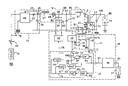
particularly to FIGURE 1 thereof, there is shown an
automotive ignition system including a DC-DC voltage
converter 10 acting as a DC power source, a ignition
transformer 11 having a primary winding 12 and a
secondary winding 13, a spark plug 11 connected with
the secondary winding 13, a ignition capacitor lS
electrically connected to the primary winding 12, a
charge circuit 16 for charging the ignition capacitor
15 from the DC-DC voltage converter 10, a discharge
.circuit 17 for discharging the ignition capacitor 15 to
the primary winding 12, and control circuit 18 for
operating the charge circuit 16 and the discharge
circuit 17 in proper timed se~uence during the demanded
firing duration. The reference numerals 19, 20, 21
indicate respect:ively, a battery for supplying the
power (DC 12V) to the circuits 10 and 18, a ignition
switch and a breaker point.
The DC-DC converter 10 includes a swinging choke
inverter 22, a diode 23 and a first capacitor 24 having
a large capacitance, for example, 100 ~F). The DC-DC
converter 13 stores a predetermined voltage generally
DC ~00 (V) which is higher than that of battery 19 due
~30~a~4
-15-
to the functioning of the swinging choke inverter 22.
The voltage of the first capacitor 24 is regulated to
the predetermined value because the voltage at the
first capacitor 24 is feedback to the swinging choke
inverter 22 via a feedback line 25. Therefore, if the
voltage at the first capacitor 24 is droppedh swinging
choke inverter 22 is driven by the feedback signal so
as to replenish the voltage at the first capacitor.
24. ~n output voltage V26 of DC-DC voltage converter
10 exists at junction 25.
The charge circuit 16 includes a first inductor 27
of inductance 100 (~H), a first thyristor 28 operated
as a charge switch, and a capacitor 29 and resistor 30
for increasing t-he noise margin in order to drive the
first thyristor 28.
The discharge circuit 17 includes a choke coil 31
of inductance 1 (mH), a second thyristor 32, a diode
33, and a capacitor 34 and resistor 35 for increasing
the noise margin to drive the second thyristor 32 and
to detect the on-off state of the second thyristor 32.
The control circuit 18 includes a firing duration
decision circuit 36 for deciding the demanded firing
duration, a detecting circuit 37 for detecting on-off
state of the second thyristor 32, a repetition rate
control circuit 38 for operating the charging circuit
15 and the discharging circuit 17 with a proper timed
130~824
-15-
sequence during the demanded firing duration, a first
driving circuit 38' for driving the first thyristor 28
and a second driving circuit 39 for driving the second
thyristor 32.
As shown in FIGURE 2, the firing duration decision
circuit 36 includes an input protection and filter
circuit 40, an inverter 41, a one-shot multivibrator
42, a ramp generator-43, a peak hold circuit 44, a .
voltage follower 45, a voltage divider 46, a comparator
47, a peak cancel circuit 48, and an external spark
crank angle controller 49 for controlling the output of
the voltage divider 46 in response to a external
commanded signal being, in turn, changed in response to
an engine condition, for example, the engine
temperature and load conditions, etc.
At a junction 50, the breaker point 21 generates a
signal V50. The period T (of the signal V50) is
defined by the following equation:
T = n20 (sec.)
where n: engine speed (rpm)
m: number of cylinder
During the period T of the signal V50, the signal
V50 is at a high level during time TA when the breaker
point 21 is to be opened and is at a low level during
time TB when the breaker point 21 is to be closed.
~.3~82AL
The rising edge of the high level of the signal
V50 indicates the starting time of the firing duration,
and the period T of the signal V50 is inversely
proportional to the engine speed.
The signal V50 is transmitted to the one-shot
multivibrator 42 and the peak cancel circuit 48 via the
circuit 40 and inverter 41. Th~e one-shot multivibrator
42 generates a trigger voltage V51 at a point 51 when
the high level of signal V50 rises, as shown in FIGURE
3~. Upon the occurrence of signal V50, the ramp
generator 43 starts to charge capacitor 52 with
predetermined time constant. The voltage V53 at a
junction 53 is the charged voltage of capacitor 5~.
This voltage increases in response to the lapsed time
of the signal V50, as shown in FIGURE 3C. The voltage
V53 is transmitted to an inverting input of the
comparator 47.
(~ A capacitor 54 of peak hold circuit 44 mèmorizes
the peak value of a previous voltage V53 and generates
a voltage V55 as shown in FIGURE 3C at a junction 55.
The voltage V55 is transmitted to the voltage divider
46 via the voltage fol.lower 45. The voltage divider 46
divides the voltage V55 to 10-15 percent thereof and
generates a voltage V56 at a junction 56.
The comparator 47 compares the voltage V56 with
the voltage V53 and generates a firing duration signal
~30~824
-18-
V57 at a junction 57 until the voltage V56 is higher
than the voltage V53. The duration TD in the firing
duration signal V57 as shown in FIGURE 3D indicates the
demanded firing duration. The duration TD is
proportional to Period T and expressed as follows:
TD = R.T K : dividing ratio of divider
(10-15 percent)
A transistor 58 in the peak cancel circuit 48 is
turned on when the signal V50 is no longer at a high
level thus cancelling the voltage V55 and replacing it
with the voltage V53 via a peak detector 59 being
formed by an operational amplifier 60 and a diode 61
until signal V50 reaches a high level as shown in
FIGURE 3A. iqhen the high level of the signal V50
occurs, the transistor 58 is turned off and thus the
voltage V55 is kept to the peak value of voltage V53.
The firing duration decision circuit 36 generates the
firing duration signal V57 in precise response to the
engine speed due to the firing duration signal V57
being based on the signal V50 which indicates the
engine speed.
The repetition rate control circuit 38, as shown
in FIGURE 1, includes one shot multivibrators 6~, 63
and 64 for generating a trigger when the rising edge of
an input signal is detected, a delay circuit 65 for
delaying the 'alling edge of illpUt signal, delay
~1301824
circuit 66 and 67 for delaying the rising edge of an
input signal, an OR circuit 68 and an AND circuit 69.
The firing duration signal V57 at the output of
circuit 36 is applied to the one-shot multivibrator 52
and to one input of AND circuit 69. The one-shot
multivibrator 62 detects the rising edge of signal V57
and qenerates the output voltage trigger V70 shown at a
point 7~ in FIGURE 1 and as V70 in FIGURE 4B.
The trigger V70 is applied to the AND circuit 69
via the OR circuit 68. The AND circuit 69 generates a
trigger V71 as shown in FIGURE 4C. This trigger V71
operates the second thyristor 32 via the second drive
circuit 39. The delay circuit 65 detects the output
V72 at the point 72. The output V72 is at a high level
when the second thyristor 32 is to be turned off,
while, on the other hand, the output V72 drops to a low
level when the second thyristor 32 is to be turned on,
as shown in FIGURE 4D. The delay circuit 65 detects
the falling edge of output V72 and generates a signal
V73 at output 73 with a delay time tdl as shown in
FIGURE 4E. The delay circuit 66 detects the rising
edge of signal V73 and generates a signal V74 at output
74 with delay time td2 as shown in FIGURE 4F. The
signal V74 is applied to the one-shot multivibrator 64
and the delay circuit 67. The one-shot multivibrator
64 generates a trigger signal V75 with pulse width tw3
130~824
~20-
at place 75. This trigger signal V75 operates the
first thyristor 28 via the first drive circuit 38'.
The delay circuit 67 detects the rising edge of
signal V74 and generates a signal V76 at point 76 with
the delay time td3 as shown in FIGURE 4H. The signal
V76 is applied to the one-shot multivibrator 63. The
one-shot multivibrator 63 generates a trigger signal
V77 with pulse width tw2 at place 77 as shown in FIGURE
4I. This trigger V77 is applied to the AND circuit 69
via the OR circuit 68. Therefore, during signal V57 is
at a high level trigger V71 is generated by the trigger
voltages V70 and V77. ~owever, if the firing duration
signal V57 goes to low level, the trigger V71 is not
generated by the function of the AND circuit 69.
Likewise, the trigger 75 is not generated when the
firing duration signal V57 goes to low level. In the
repetition rate control circuit 38 of FIGURE 1, the
trigger V75 is generated after the off state of second
thyristor 32 is detected.
The detecting circuit 37 for detecting the on-off
state of second thyristor 32 includes a transistor 78,
a capacitor 79 and resistor 80 for increasing noise
margin to detect the on-off state of the second
thyristor 32. When the hold current for holding the on
state of second thyristor 32 flows between the anode
and the cathode o~ second th~ristor 32, the second
130~24
-21-
thyristor 32 is kept in the on state in spite of the
absence of trigger V71. During the on state oF second
thyristor 32, the gate voltage V81 of second thyristor
32 at the junction 81 is sufficient to turn the
transistor 78 on. Therefore, the ou~ut V72 of
detecting circuit 37 changes to the high level voltage
from the low level voltage when the second thyristor 32
changes to the off state from the on state, as shown in
FIGURE 4D.
The gate voltage V81 of second thyristor 32 has
temperature coefficient. The transistor 78 has a
temperature coefficient of its P-L~ junction (hase-
emitter) nearly equal to that of the P-N junction
(anode-cathode) in the second thyristor 32. As the
result, the detecting of the on-off state of the second
thyristor 32 is compensated in spite of temperature
change.
( FIGURE 5 shows the first driving circuit 38' in
detail, the first driving circuit 38' is formed with a
conventional pulse transformer. The first driving
circuit 38' receives the trigger signal V75 and
generates a trigger V82 for driving the first thyristor
32 between junctions 82 and 83.
FIGURE 6 shows the second driving circuit 39 in
detail, the second driving circuit 39 receives ~he
trigger signal V71 and generates a trig9er signal V
~30~ 4 -~
-22-
for driving the second thyristor 32 between the
junction 81 and the grounded junction 84.
As shown in FIGURE 7 when the trigger signal V
is applied between junctions 81 and 84, the second
thyristor 32 is turned on whereby the gate voltage V
of second thyristor 32 changes as shown in FIGURE 7B.
Consequently, the current I85 for charging a stray r
capacitor, defined by windings 12 and 13 an~ the spark
plug 14 flows at output 8S from the ignition capacitor
15. As the result, the stray capacitor is charged and
the voltage V86 at output 86 increases and reaches the
breakdown voltage VB in the gap of spark plug 14 as
shown in PIGURE 7H. The breakdown in gap sf spark plug
14, is such that the electric charge of the stray
capacitor 186 is discharged quickly and is reflected as
a current between gap of spark plug 11 shown in FIGURE
7G. After the breakdown in the gap of spark plug 14,
as sho~n in FIGURES 7G-7H, the voltage V86 drops to the .
sustaining voltage Vs (1 - 3 kv), and the spark current S.
I86 flows between the gap of s2ark plug 1~ with the
resonant frequency defined by the capacitance of the
ignition capacitor 15 and the inductance of the choke
coil 31. When the spark current I86 becomes zero, the
voltage V87 at junction 87 is at its maximum negative
value, as shown in FIGURE 7C. Until now the second
thyristor 32 has been turned on, but it is turned off
~3~la~4
-23-
by the voltage V87 which provides an inverse bias to
the second thyristor 32. Instead of the seeond
thyristor 32 being turned off, the diode 33 is now
turned on, and as a result the spark current I86 flows
in the reverse direction. This spark current I86 also
has the resonant frequency noted above and ch,arges the
ignition eapacitor 15. The residual voltage Vr remains
at the ignition capaeitor 15, whieh waveform in voltage
V87 being shown in FIGURE 7C.
Subsequently, the trigger V82 is supplied to the
first thyristor 28 with delay time td2 after the second
thyristor 32 is turned off, and the first thyristor 28
is turned on whereby a eharge eurrent I88 flows at the
output 88, as shown in FIGURE 7E. The eharge current
I88 is the resonance current, defined by capaeitanee of
the eapaeitor 15 and inductanee of the first inductor
27. As a result of this resonanee eurrent, the
ignition eapacitor 15 is charged and awaits the next
oeeurring discharging by the trigger signal V81. When
the eharge eurrent I88 beeomes zero, the voltage V87 of
ignition eapacitor 15 is higher than the voltage V26 of
first capacitor 24, whereby the first thyristor 28
becomes reverse biased. The instant that the reverse
current flows, the first thyristor 28 is to be turned
ofE.
~301a2~L -
--24-
FIGURE 8 shows the time relation among the signal
V50 of breaker point 21, the firing duration signal
V57, the spark current I86 and the voltage V26 at the
capacitor 24. The voltage V26 slightly decreases
during the firing duration, but the voltage V26
recovers to the predetermined value during the non-
firing duration. Therefore, the average output power
of the DC-DC voltage converter 10 is decided by the
spark duty Ds indicates as follows:
DS = TD
where T: the period in the signal V50 of breaker
point 21
TD: the firing duration
Ds is 0.1 to 0.15 for a typical application.
Therefore, the output power of the DC-DC voltage
converter 10 is not required to be high.
. FIGURE 9 shows the ignition transformer 11 in
; detail. The ignition transformer 11 is a low leakage
inductance transformer which has no air gap beween the
opposed surface of a core 90 at the center of the core
90. Although ignition transformer 11 has low leakage
induction, the combination of the transformer 11 with
the choke coil 31 provides a proper spark duration for
one shot and a proper spark current I86 so that the
inductance of the choke coil 31 is selected to be a
suitable value with respect to the capacitance of the
~30~824
-25-
ignition capacitor 15. It is also to be noted that the
sectional area of the core 90 is reduced because the
voltage across the primary winding 12 is sufficient low
during the sustaining voltage period of the spark plug
when compared with conventional air gap ignition
transformer operation.
Furthermore, the sectional area of the core 90 is
inversely proportional to the resonant frequency of the
spark current I86 defined by the capacitance of the
ignition capacitor 15 and the inductance of the choke
coil 31. Thus, the size of the ignition transformer 11
can be decreased in response to an increase in the
resonant frequency.
FIGURE 10 shows another embodiment of the
detecting circuit 37 for detecting the on-off state of
second thyristor 32. In this embodiment, the
transistor 78 is replaced with a comparator 92 having
an inverting input connected to the junction ~31 as
shown in FIG~RE 1 and a non-inverting input connected
to a junction 93. A voltage V93 caused at the junction
93 is the divisional voltage being defined by a diode
94 and a register 9S. The voltage V93 is set to the
predetermined value which is lower than that of the
gate voltage V81 when the second thyristor 32 is turned
on and is 'nigher than that of the voltage V8l when the
second thyristor 32 is turned off. Furthermore, the
~30~8~4
temperature coefficient in the P-~ (anode-cathode)
junction of diode 94 is equal to that of the P-N
(anode-cathode) junction in the second thyristor 32.
ThereEore the detecting circuit 37 in FIGURE 10 has the
temperature compensation function similar to that of
FIGURE 1. Consequently the output of the comparator 92
is equal to the voltage V72 as shown in FIGURE 4.
The arrangement.of FIGURES 11 and 12 provides for
the detecting of on-off state of the second thyristor
32.
In the arrangement of FIGURE 11, a diode 97 is
installed between the cathode of second thyristor 32
and the grounded junction 84. The junction 81 at the
gate end of thyristor 32 is connected to the resistor
80 of the detecting circuit 37 in FIGURE 1 or FIGURE
10 .
, In the arrangement as shown in FIGURE 12, a diode
98 and a resistor 99 is installed in parallel between
the cathode of second thyristor 32 and the grounded
junction 84. The gate of second thyristor 32 is
connected to the output of second driving circuit 39 in
FIGURE 1 and the junction 100 in FIGUR2 12 is connected
to the resistor 80 in the detecting circuit 37 in
FIGURE 1 or FIGURE 10.
FIGURE 13 shows another embodiment oE the
repetition rate control circuit 38. In this embodiment
~30~82A
-27-
of circuit 38 the trigger V75 for operating the first
thyristor 28 is first generated when the repetition
rate control circuit 38 receives the firing duration
signal V57 (the repetition rate control circuit 38 in
FIGURE 1 first generates the trigger V71 for operating
the second thyristor 32 when the circuit 38 receives
the firing duration signal V57),
The repetition rate control circuit 38 in FIGURE
13 includes an AND circuit 102, a one-shot
multivibrator 103, a monostable multivibrator 104, a
one-shot multivibrator 105 and delay circuits 106 and
107. The connection between the circuits 102, 103,
104, 105, 106, 107 and the points 57, 71, 72 and 75 is
as shown in FIGURE 13.
The AND circuit 102 receives the firing duration
signal V57. The one-shot multivibrator 103 detects the
rising edge of voltage V1~8, which is the output of AND
circuit 102, and generates the tigger V75 for operating
the first thyristor 28 as shown in FIGURES l~C. The
monostable multivibrator 104 detects the rising edge oE
the trigger V75 and generates a signal V109 at output
109 during the time tpl of the time constant thereof,
The one-shot multivibrator lnS detects the falling
edge of the signal '~109 and generates the trigger V
for operating the second thyristor 32.
130~824
-23-
The delay circuit 106 detects the falling edge of
signal V72 corresponding to the on-off state of second
thyristor 32 (the high level voltage of signal V72
indicates the off state of second thyristor 32) and
generates a signal V110 at point 110 with delay time
tdl. The delay circuit 107 detects the rising edge of
signal V110 and generates a signal Vlll at place 111
with delay time td2. The signal Vlll is supplied to
the AND circuit 102.
The relation between each shape in the signals
output in FIGURE 13 and their timing is shown in
FIGURES 14A-14H.
The discharging circuit 37 can take the form oE
different configurations depending upon the desired
shape of spark current I86.
If a spark current I86 is desired to be a half
sine wave as shown in FIGURE 16F, the circuit disclosed
in FIGURE lS is utilized as the discharge circuit. The
discharge circuit in FIGURE 15 deletes the diode 33
disclosed in FIGURE 1 whereby the reverse current does
not flow through the ignition transformer 11, and the
spark current I86 becomes a half sine wave. Other
ltages V81~ V87~ V82 and V86 currents I88, I85 and
I86 caused at places 81, 87, 82, 88, 85 and 86 and
their timing are as shown in FIGURES 15A-15G.
~30~824
-29-
Furthermore, if a spark current I86 is a saw tooth
wave as shown in FIGURES 18G and 20F, the circui.s
disclosed in FIGURES 17 and 19 are utilized as
discharge circuits. In FIGURE 17, a Zener diode 120
and a diode 121 is installed between the ignition
capacitor 15 and the anode of second thyristor 32 and
the diode 33 disclosed in FIGUR~ 1 is deleted.
In FIGURE 19, the Zener diode 120 and the diode
121 in FIGURE 17 are installed between the junctions 87
and 84. FIGURES 18A-18H and 20A-20G show the voltages
V81, V87, V82, V86 with the currents I8~, I85 and I86
at places 81, 87, 82, 88, 85 and 86 indicated as in
FIGURES 17 and 19.
The current Ia, as sho~ln in FIGURE 18F, represents
the current flowing through the Zener diode 120 and
diode 121 in FIGURE 19.
; As shown in FIGURES 7C and 16B, the residual
i voltage Vr remains at the junction 87 connected to the
ignition capacitor 15 disclosed in FIGURES 1 and 15
prior to recharging of the ignition capacitor 15. In
the discharge circuit 37 in FIGURE 1, the residual
voltage Vr is positive. In turn, in the discharge
circuit 37 in FIGURE 15, the residual voltage Vr is
negative.
These residual voltages Vr are undesirable because
: the charged voltage in the ignition capacitor 15 in
130~32~
-30-
next charging changes in response to the residual
voltage Vr. For example, the charged voltage V87 in
the ignition capacitor 15 in FIGURE 1 changes according
to residual voltage Vr as shown in the solid line in
FIGURE 23, and, in turn, the charged voltage V87 in the
ignition capacitor 15 in FIGURE 15 changes according to
residual voltage Vr as shown.in the solid line in
FIGURE 27. As the result for negative residual
voltage, as the situation repeats itself, there is no
limit to the increase in the charged voltage V87 as
shown in FIGURE 26.
Therefore, if either a positive or negative
residual voltage Vr appears, the combustion
stabilization of the engine is not accomplished or one
of the elements such as the second thyristor 32 of the
discharge switch becomes damaged.
But, in the discharge circuit in FIGURES 17 and
19, the residual voltage is negligihle as shown in
FIGURES 18B and 20B.
In order to remove the influence of the residual
voltage Vr and to regulate the charged voltage V87
during charging time, a buffer circuit is connected to
the charging circuit 15.
A buf~er 130, as shown in FIGURE 21, is available
against the positive residual voltage Vr. The buffer
~30~l324
-31-
130 includes a second inductor 131 ( 200 ~H) and a
resistor 132 and a second capacitor 133 (2~3 ~F) which
is two to three times greater than capacitor 15 (1 uF)
and is electrically connected to the DC-DC voltage
converter 10, the charging circuit 16 and the ignition
capacitor 15 as shown in FIGURE 21.
Current I134 which is outpyt at 134 and a voltage
V135 at the junction 135 in FIGURE 21 is as shown in
FIGURE 22F-22G. By the operation of this current I134
and voltage V135, the charged voltage V87 of the
ignition capacitor lS, during charging, is constant and
does not have residual voltage influence which is shown
as a chained line in FIGURE 23.
A buffer 140 as shown in FIGURE 24, is available
against a negative residual voltage Vr. The buffer 140
includes a third inductor 141 (25 ~) and a diode 142
and is eletrically connected to the charging circuit 15
as shown in FIGURE 24. 3y the operation of the buffer
140, when the first thyristor 28 is turned on, the
negative residual voltage at ignition capacitor 15 is
passed through the second inductor 141 and the diode
142. As the result, the current I88 flowing through
the portion 88 in FIGURE 24 is the total of a current
I143 flowing through the second inductor 141 and a
current I144 flowing through the first inductor 27.
The resonant frequency produced by the inductor 141 and
1301~32~
-32-
the capacitor 15 is of a high value so that the
inductance value of the inductor 141 is selected to be
smaller than the inductance value of the inductor 27
(200 micro H)
Thus, the buffer 140 charges the capacitor 15
faster than the inductor 27. In actuality, the buffer
circuit 140 acts by reversing the polarity of the
capacitor 15. Consequently, the negative residual
voltage Vr is reduced to a negligible value when the
charging current I144 from the inductor 27
approximately reaches its peak value. Thus, the
charged voltage V87 of ignition capacitor 15 is
constant and does not have the negative residual
voltage influence which is shown as a chained line in
FIGURE 27.
FIGURE 28 shows a preferred embodiment of a non-
mechanical distributor ignition system in a four
cylinder engine applied to the present invention.
In this system, the spark current is in the shape
of a half sine wave and the buffer 140 noted above is
utilized. Each ignition transformer lla, llb, llc and
lld is arranged respectively with each spark plug 14a,
14b, 14c and 14d. Each second thyristor 32a, 32b, 32c
and 32d, and each drive circuit 39a, 39b, 39c and 39d
for driving each thyristor 32a, 3 b, 32c and 32d is
arranged respectively with ignition transformer lla-
1301~il2~
-33-
lld. The detecting circuits 37a, 37b, 37c, and 37d for
detecting on-off state of each thyristor 32a, 32b, 32c
and 32d are arranged respectively with thyristor 32a,
32b, 32c and 32d. The ignition trnsformers lla, llb,
llc and lld are electrically connected to the ignition
capacitor 15 via the choke coil 31. A engine computer
150 generates a signal V152 at the output 152 in FIGURE
28 which is based on the output oE a crank angle sensor
151 for detecting the degree of rotation of crankshaft
153 in the engine. The signal V152 is similar to the
signal V50 generated by the breaker pOillt 21. A cam
angle sensor 154 detects the angle of the cam shaft
156, which is a source signal to select the one of four
spark plugs for firing, and which generates a signal
V154 as an output as shown in FIGURE 30C. The signal
1152 is applied to the firing duration decision circuit
36 and a cylinder selecting circuit 155. Also the
signal V154 is applied to the cylinder selecting
circuit 155. The cylinder selecting circuit 155 is
formed with a our stage static shift register as shown
in FIGURE 29. Each output 155a, 155b, 155c and 155d in
FIGURE 29 has associated therewith the voltages V155a,
V155b V155C and V156d, reSpeCtively~ as shown in
FIGURES 29D-29G. Each voltage V155a, V155b V155c
V155d is applied to each driving circuit 39a, 39b, 39c
and 39d via each AND circuit 157a, 157b, 157c and
~301~%4
-34-
157d. Each AND circuit 157a, 157b, 157c and 157d
receives the trigger V71 Eor operating the thyristors
32a, 32b, 3~c and 32d from the repetition rate circuit
38. The reference numeral 158 in FIGURE 29 indicates a
one-shot multivibrator detecting the rising edge of the
signal V152-
Consequently, tne selecting spark plug by the
signal V155a~ Vlssb~ Vl55c and V155d produc
ignition spark train in proper timed sequence during
the demanded firing duration.
In the drawings, the reference symbols Vc and VB
indicate a regulated DC voltage o' 5 volts and the DC
voltage of battery 19 of 12 volts.
Obviously, numerous modifications and variations
of the present invention are possible in light of the
above teachings. It is therefore to be understood that
within the scope of the appended claims, the invention
may be practiced otherwise than as specifically
described herein.