Note : Les descriptions sont présentées dans la langue officielle dans laquelle elles ont été soumises.
130~849
-- 1 --
BACRGROUND O~ TH~ INVENTION
1. Field of the Invention
The present invention generally relates to a
power saving arrangement and power saving method for use in
subsidiary unit, such as a handset unit, which com~unicates
with a base unit in response to the detection of an ID
signal produced from the base unit.
2. De~cription of the Prior Art
Recently, many developments have been made on
pocket size receiver, for example, cordless telephones,
radio pagers or portable telephones, which can effect
wireless communication between a base unit and a handset
unit.
In these receivers referred to above, portability
is particularly emphasized, and accordingly a various
circuit arrangements are incorporated in a monolithic IC or
the like driven by a battery. Thus, from the viewpoint of
power saving, a standby mode is presented. When the
standby mode i~ established, the electric power from the
battery is supplied to the various circuits intermittently
in pulses having a predetermined frequency, ~o that the
handset unit can detect and analyze the ID signal
transmitted from the base unit. When the ID signal is
detected, the handset unit is changed from the standby mode
to the use mode to detect data signal following the ID
signal, thereby starting communication between the handset
~23018~9
unit and the base unit. Thus, during the standby mode, the
power consumption is saved.
BRIBF D~3SCRIPTION t)F THE: DRl~WINGS
These and other objects and features of the
S present invention will become apparent from the following
description taken in conjunction with a preferred
embodiment thereof with reference to the accompanying
drawings, through which like parts are designated by like
reference numerals, and in which:
Fig. 1 is a block diagram of a power saving
circuit arrangement according to a preferred embodiment of
the present invention;
Fig. 2 is a circuit diagram of a power saving
circuit arrangement of Fig. 1;
Fig. 3 is a flow-chart showing the operation of
the power saving circuit arrangement of the present
invention; and
Fig. 4 is a circuit diagram of a prior art power
saving circuit arrangement of a received wave processing
,() circuit.
An example of a prior art power saving
arrangement is shown in Fig. 4.
The circuit shown in Fig. 4 includes a battery 1
which i~ a power source for the handset unit such as in a
cordless phone system, a radio frequency amplifier 2, a
mixing circuit 3, a local oscillatox 4, an intermediate
frequency amplifier 5, a demodulator 6, a signal strength
detecting circuit 7 which operates as a detector for
A
30~849
detecting the signal level of the received signal, and a
waveform shaping circuit 9-for shaping the ID signal fro~
the demodulator 6. A CPU 10 function~ to analyze the
pattern of received ID signal and to change the mode
between standby mode and use mode. During the standby
mode, CPU 10 produces a power saving signal PSS to
operation control circuit 11 which then produces power in
pulses having a predetermined frequency, and supplies the
pulsating power to various circuit~. Such an intermittent
power supply to various circuits is not sufficient to
properly process the data signal from the base unit, but is
sufficient to analyze the ID signal. Thus, during the
standby mode, power necessary to analyze the ID signal is
constantly supplied to the various circuits, such as to IF
amplifier 5, demodulator 6 and waveshaping circuit 9. When
the pattern of the detected ID signal coincides with the
pattern stored in CPU 10, the mode i8 changed from the
standby mode to use mode. Under the use mode, the power
saving signal PSS is cut off ~o that the operation control
circuit 11 continuously provides the full power to the
various circuits.
According to the prior art power saving
arrangement, since the intermediate frequency amplifier
circuit 5, demodulator circuit 6 and waveform shaping
circuit 9 are continuously operated even during the ~tandby
mode to analyze the ID signal, there is such a problem that
the power consumption during the standby mode is still
quite high.
8UMMARY OF THB INVBNTION
Accordingly, the present inv~ntion has been
A
... ...
_ 4 ~301849
developed with a view to substantially eliminating ~he
above-described problem in the prior art, and has for its
essential ob~ect to provide an improved power saving
arrangement and power saving method which can further save
the power during the standby mode.
In accomplishing these and other ob~ects, a power
saving arrangement according to the present invention
comprises: power control circuit for selectively producing
a full power and a reduced power; a processing circuit
means for receiving and processing said data signal when
the full power is applied thereto, and for detecting the
level of a received signal when the reduced electric power
is applied thereto; detecting circuit means, connected to
said processing circuit means, for detecting data signal
when the full power is applied thereto, and for detecting
only ID signal when the reduced power is applied thereto;
first switching means for making and braking a power supply
path to said detecting circuit means from said power
control circuit; and control means for controlling said
power control circuit and said first switching means to
establish either one of first standby mode, second standby
mode and use mode such thats under the first standby mode,
said first switching means breaks the power supply to said
detecting circuit means and, at ,the same time, power
control circuit produces the reduced power to said
processing circuit means, ready to detect the level of said
ID signal; under the second standby mode as established
when said control mean~ detects that received signal level
exceeds a predetermined level, said first switching means 3~ makes the power supply to said detecting circuit means and,
~301~!349
at the same time, power control circuit produces the
reduced power to said processing circuit means and also to
said detecting circuit means, ready to detect and read the
pattern of said ID signal; and under the use mode a~
S established when said control means detects that said ID
signal has a predetermined pattern, said first switching
means makes the power supply to said detecting circuit
means and, at the same time, power control circuit produces
the full power to said processing circuit means and also
to said detecting circuit means, ready to detect and read
said data signal.
In a further aspect the invention provides a
power saving arrangement for use in a subsidiary unit
which communicates with a base unit in response to the
detection of an ID signal leading data signal which are
produced from said base unit and received by said
subsidiary unit, said power saving arrangement comprising;
power control circuit for selectively producing a full
power and a reduced power; a processing circuit means for
receiving and processing said data signal when the Eull
power is applied thereto, and for detecting the level of
the received signal when the reduced electric power is
applied thereto; detecting circuit connected to said
processing circuit means for detecting said data signal
when the full power is applied thereto, and for detecting
only said ID signal when the reduced power is applied
thereto; first switching means for making and breaking a
power supply path to said detecting circuit means from
said power control circuit; and control means responsive
to a signal representing the level of the received signal
A
,.
~3~1B49
", ~
obtained from said processing means and also to said ID
signal ob~ained from said detecting circuit means for
controlling said power control circuit and said first
switching means to establish either one of first standby
mode, second standby mode and use mode such that; under
the first standby mode, said first switching means breaks
the power supply to said detecting circuit means and, at
the same time, said power control circuit produces the
reduced power to said processing circuit means, ready to
detect the level of the received signal; under the second
standby mode as established when said control means
detects that the received signal level exceeds a
predetermined level, said first switching means makes the
power supply to said detecting means and, at the same
time, power control circuit produces the reduced power to
said processing circuit means and also to said detecting
circuit means, ready to detect and read the pattern of
said ID signal, and under the use mode as estahlished when
said control means detects that said ID signal has a
predetermined pattern, said first switching means makes
the power supply to said detecting circ~it means and, at
the same time, power control circuit means and also to
said detecting circuit means, ready to detect and read
said data signal.
Also, according to the present invention, power
saving method comprises the steps of: providing a reduced
power to said processing circuit means and providing no
power to said detecting circuit means, when ID signal and
data signal are not present, ready to detect the level of
A
~- 5 130~849
said received signal by said processing circuit means;
providing said reduced power to said processing circuit
means and also to said detecting circui~ means, when the
detected received signal level exceeds a predetermined
level, ready to detect the pattern of said ID signal by
said detecting circuit means; and providing full power to
said processing circui~ means and also to said detecting
circuit means, when the detected ID signal pattern i~
identical to a predetermined pattern, ready to detect and
lo reproduce the data signal.
In a yet further aspect the invention provides a
power saving method for use in a subsidiary unit which
communicates with a base unit in response to the detection
of an ID signal leading data signal which are produced
from said base unit, said subsidiary unit having a
processing circuit means for receiving and processing said
ID signal and data signal, control means for generating a
control signal in response to output signals from said
processing circuit means and said detecting circuit means,
and power control means for generating either one of a
reduced power signal and a full power signal in response
to said control signal, the power saving method comprising
the steps of; providing a reduce power to said processing
circuit means and providing no power to said detecting
circuit means when said ID signal and data signal are not
present, being ready to detect the level of the received
signal by said processing circuit means; providing said
reduced power to said processing circuit means and also to
said detecting circuit means from power control means when
~g ;
- 6 _ 130~8~9
the detected received signal level exceeds a perdetermined
level and being ready to detect the pattern of said ID
signal by said detecting circuit means; and providing full
power to said processing circuit means from power control
means when the detected ID signal pattern is identical to
a predetermined pattern and being ready to detect and
reproduce the data signal.
D~SCRIPTION OF PREFEM ED ~MBODIMENT
Referring to Figs. 1 and 2, a power saving
circuit arrangement and the power saving method according
to the present invention will be described hereinbelow.
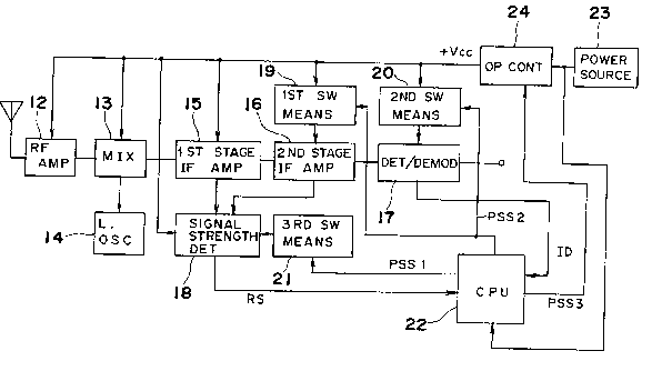
In Figs. 1 and 2, reference numeral 12 represents
a radio frequency amplifier circuit for amplifying waves
received by an antenna of a cordless phone system or the
like; 13 is a mixing circuit for converting high frequency
signals to intermediate frequency signals; 14 is a local
oscillator; 15 is a first stage intermediate frequency
amplifier; 16 i~ a second ~tage intermediate frequency
amplifier; and 17 is a detector/demodulator for detecting
audio ~ignals from the intermediate frequency signals,
which are connected in series. Detector/demodulator 17
also produces an ID signal which has been produced from the
base unit (not shown) and processed and amplified through
circuits 12, 13, 14, 15, 16 and 17. The ID signal from
cixcuit 17 is applied to a CPU 22 in which it is detected
whether or not the detected ID signal is the same as the ID
signal assigned to the handset unit. Preferably, as shown
in Fig. 2, the ID signal is formed by a waveform shaping
13018~9
-- 7 --
circuit 25 which filters the output signal from the
demodulator 17 and shapes up the waveform.
A signal strength detecting circuit 18 receives
signals from first and second stage amplifiers 15 and 16 to
generate an RS signal indicative of the strength of the
intermediate frequency signals produced from the first and
second stage amplifiers 15 and 16. The generated RS signal
is applied to CPU 22.
An electric power to each of the circuits 12, 13,
14, 15, 16, 17 and 18 i8 supplied from a power source 23
through an operation control circuit 24. A power ~ource
23 i8, for example, a battery when the processing circuit
i8 employed in a handset unit of a cordless phone system.
Furthermore, according to the present invention, the
electric power to the second stage amplifiers 16 and
modulator 17 are further controlled by first and second
switching means 19 and 20, respectively. As
diagrammatically shown in Fig. 2, the first switching means
19 includes two switches SWl and SW2, and the second
switching means 20 includes a switch SW3. Also, according
to the present invention, the electric power to a portion
of signal strength detecting circuit 18 is further
controlled by a third switching means 21, which is
diagrammatically shown by a switch SW4 in Fig. 2.
CPU 22 produces power saving signals PSS1, PSS2
and PSS3 which are applied to third switching means 21,
first and second switching means 19 and 20, and operation
130~849
-- 8 --
control circuit 24, respectively. The power saving signals
PSSl and PSS2 control ON/OFF operations of the first and
second switching means 19 and 20, and the power saving
signal PSS3 controls operation control circuit 24 such that
operation control circuit 24 generates an intermittent
operating voltage +Vcc in pulses having a predetermined
frequency when the power saving signal PSS3 is present, but
it generates a continuous operating voltage +vcc when the
power saving signal PSS3 is not present.
By using the RS signal and ID signal/ CPU 22
determines the mode which is either a first standby mode,
a second standby mode or a use mode.
The operation of the power saving circuit shown
in Figs. l and 2 will be described hereinbelow with
reference to the flow chart of Fig. 3. In Pig. 3, the
operation under the first standby mode is indicated by MDl
covering steps P1-P3, the second ~tandby mode by MD2
covering steps P4 and P5, and the use mode by MD3 covering
steps P6-P8, re~pectively.
Under the first standby mode MDl, power saving
signals PSSl, PSS2 and PSS3 are produced. Thus, at step
P1, by the power saving signal PSS2, the first and second
switching means 19 and 20 are both turned off so that the
electric power from the operation control circuit 24 to
each of second stage intermediate frequency amplifier 16
and detector/demodulator 17 is cut off. Also, by the power
saving signal PSS1, the third switching means 21 is turned
130i~349
g
off so that the elect~ic power to the portion of signal
strength detecting circuit 18 is cut off.
Then at step P2, by the power saving signal PSS3,
operation control circuit 24 is so operated as to produce
pulsating power at a predetermined frequency (also referred
to as an intermittent voltage (+Vcc) power). Thus, first
stage intermediate frequency amplifier 15, mixing circuit
13, local oscillator 14 and radio frequency-amplifier
circuit 12 and a portion of signal strength detecting
circuit 18 are operated intermittently.
Thus, under the first standby mode MDl, no power
is consumed in circuits 16 and 17 and reduced power is
consumed in circuits 12, 13, 14, 15 and 18, the rate of
reduction being dependent on the duty ratio of the
intermittent voltage power as set in operation control
circuit 24. Accordingly, by the half powered circuits 12,
13, 14, 15 and 18, the signal received by the antenna will
not be processed properly, but is processed sufficiently to
detect the level of the received signal. Such a detection
of the received signal level is carried out particularly in
signal strength detecting circuit 18 which then produces RS
signal representing the received signal level.
At step P3, it is detected in CPU 22 using the
RS signal whether or not the received signal level is
greater than a predetermined level. If no signal is being
received or if the receiving signal level i8 lower than the
predetermined level because, e.g., the handset unit is far
13~849
-- 10 --
from the base station, step P3 for the detection of RS
signal is repeated. On the contrary, if it is detected
that the received signal level is greater than the
predetermined level, the program advances to step P4 to
enter the second standby mode MD2.
Under the second standby mode, power saving
signals PSSl and PSS2 are stopped and only the power saving
signal PSS3 is applied to operation control circuit 24.
Thus, at step P4, by the absence of power saving
signals PSS1 and PSS2r the first and second switching means
are turned on to permit intermittent voltage (+Vcc) power
supply from power control circuit 24 to second stage
amplifier 16 and to detector/demodulator 17. Thus, at this
point, all the circuits 12, 13, 14, 15, 16, 17 and 18 are
provided with intermittent voltage (+Vcc) power from
circuit 24. Such a reduced power is not sufficient to
proper detect and reproduce the audio signals, but is
~ufficient to properly detect and reproduce ID signal which
is applied to CPU 22. Then~ at step P5, it is detected in
CPU 22 whether or not the received ID signal has a pattern
which iY identical to the ID signal pattern assigned to
that handset unit. If the ID signal pattern does not
match, the program returns to step Pl to start from the
first standby mode. If the ID signal pattern does match,
the program advance~ to step P6 to enter the use mode.
Under the use mode, all the power saving signals
PSS1, PSS2 and PSS3 are stopped. By the absence of power
~301~9~9
saving signals PSSl and PSS2, the first, second and third
switching circuits are turned on, and by the absence of
power saving signal PSS3, operation control circuit 24 is
so operated as to produce full power, i.e., continuous
S voltage (+Vcc) power. Thus, circuits 12, 13, 14, 15, 16,
17 and 18 are operated with full power to properly detect
and generate the received audio signal, thereby enabling
communication between the base unit and the handset unit at
step P7. When the communication ends (step P8), the
program return~ to step Pl to start the first s~andby mode.
Thus, in the manner as described hereinabove, the
power saving operation i8 effected in two different levels,
i.e., the high percentage saving as effected under the
first standby mode MDl, and low percentage saving as
lS effected under the second standby mode MD2.
More specifically, under the first standby mode
MDl, that is, when no signal is received or when the
received signal is weak, only circuits 12, 13, 14 and 15
and a portion of circuit 18 are operated with about half or
less power, depending on the duty ratio of the pulsating
voltage (+Vcc) power, which iB sufficient to receive and
detect the level of the ID signal. Thus, under the first
standby mode MDl, the power for operating circuits 16 and
17 is saved, and also some percentage of power for
operating circuits 12, 13, 14, lS and 18 is saved.
Under the second standby mode MD2, that is, when
the received signal has a sufficiently large strength,
~ 3Q1849
- 12 -
circuits 12, 13, 14, 15, 16, 17 and 18 are operated with
about half or less power, which is sufficient to detect and
read the ID signal pattern. Thus, under the second standby
mode MD2, some percentage of power for operating circuits
12 to 18 is saved.
As has been described hereinabove, according to
the present invention, since the receiving mode is divided
into three modes, the power consumption can be reduced to
a large extent, and the life time of the battery can be
prolonged.
Although the present invention has been fully
described by way of example with reference to the
accompanying drawings, it i8 to be noted here that various
changes and modifications would be apparent to those
skilled in the art. Therefore, unless otherwise such
changes and modifications depart from the scope of the
present invention, they should be construed as included
therein.