Note : Les descriptions sont présentées dans la langue officielle dans laquelle elles ont été soumises.
~3~ 7
SOLDER CONTAINING ELECTRICAL CONNECTOR
AND METHOD FOR MAKING SAME _
BACKGROUND OF THE INVENTION
This invention relates to electrical connectors of
the type which include reflowable solder elements, and in
particular to such connectors having improved means for
retaining the solder elements in place and to methods for
forming such connectors.
A wide variety of modern electrical connectors and
pins include a mass or preform of solder mounted on or
adjacent to the pin. After the connector or pin is
mounted in place, the solder is melted in a reflow
operation in order to form a solder joint. Several
approaches have been used to position the mass of solder
in place prior to the reflow operation.
one approach is to retain the solder directly on the
pin, as for example by crimping the pin around the solder,
crimping the solder on the pin, or utilizing a solder or
other bond between the pin and the solder. The following
U.S. patents illustrate this approach: LYnch U.S. Patent
3,864,014; LYnch U.S. Patent 3,905,665; Cobauqh U.S.
Patent 3,978,569; White U.S. Patent 3,997,237; Schell U.S.
Patent 4,019,803; Seidler U.S. Patent 4,120,558; Seidler
U.S. Patent 4,203,648; MackaY U.S. Patent 4,500,149;
Seidler U.S. Patent 4,592,617; and Seidler U.S. Patent
4,679,889.
13(~
A second approach is to retain solder preforms on a
plate or strip that extends over several pins and is moved
along the axes of the pins to position the solder preforms
on the pins. See Lane U.S. Patent 3,184,830; Phohofskv
U.S. Patent 3,214,827; Pardee U.S. Patent 3,591,922; Reid
U.S. Patent 4,216,350: and Proceedings of the 11th
Electrical Insulation Conference pp. 242-245 (IEEE Publ.
73CHO-777-3EI, 1973).
A third approach is simply to slide solder preforms
alonq the pins of a connector before the connector is
mounted in place. See Harrls U.S. Patent 3,462,540; Lvnch
U.S. Patent 3,932,934; Reavill U.S. Patent 4,206,542;
Swiss Patent 653,838; and The Western Electric Enqineer,
Vol. 19, No. 2, (1975). As shown in LYnch '934, retention
strips or protrusions on the pins may be used to prevent
the solder preforms from sliding off of the pins.
A fourth approach is to hold the mass of solder in
the connector housing adjacent the pins. See Hart_an U.S.
Patents 4,641,426 and 4,663,815; Faile U.S. Patent
1,188,055; Ellis U.S. Patent 3,525,799; and Document
S/M-139 of Alphametals, Inc. (1979). The Hartman patents
disclose reservoirs formed in the connector housing to
retain solder masses around the connector pins.
Two problems often associated with solder preforms on
connectors relate to retention and reflow of the solder
preform. Solder itself is an alloy with virtually no
14265CA -2-
~3~877
memory or spring properties. For this reason, there is
little tendency for a solder preform to retain itself on a
connector pin. Of course, if a solder preform falls off
of a connector pin, the result is an unacceptable failure
to form a proper solder connection.
The second problem is related to the reflow
operation. Typically, the insulator body of the connector
tends to shield the solder preform from infrared light
used to heat the solder to reflow temperatures in infrared
soldering systems. For this reason, the insulating
housing may prevent or retard the solder preform from
reaching the temperature needed.
According to the invention, an electrical connector
is provided which has a housing that defines a bottom
surface adapted to rest on a mounting surface, at least
one side surface adjacent to the bottom surface, and a pin
mounted in the housing. The connector has at least one
channel formed in the housing. The channel opens out both
onto the bottom and side surfaces and defines a loading
axis passing through the side surface. The channel has a
first, larger cross sectional width within the housing and
a second, smaller cross sectional width adjacent to the
bottom surface. A reflowable element such as a solder
element having a third width smaller than the first width
and greater than the second width is disposed in the
channel. In this manner, the solder element is positively
14265CA -3-
13~18~7
retained in the channel against movement out of the
channel toward the bottom surface. The pin is mounted to
pass through the solder element to prevent the solder
element from moving along the loading axis out of the
channel.
A need presently exists for an improved electrical
connector that positively retains a solder preform in
place in the connector housing and prevents the solder
preform from falling out of position prior to the reflow
operation. The present invention is directed to such an
improved electrical connector, and to methods for making
such a connector.
The electrical connector of this invention provides a
mechanical interloc~ which positively retains the
reflowable or solder element in place in the housing. The
channel in the housing prevents the reflowable element
from moving in any direction other than the loading axis
of the channel, and the pin passing through the channel
prevents the element from moving along the loading axis.
As disclosed below, there are a number of distinct
approaches that can be used to assemble the connector of
this invention.
This invention provides the dual advantages of
excellent retention of the solder preform coupled with
excellent heating of the solder preform in infrared
soldering systems. The second advantage is largely due to
14265CA -4-
13V~ 7
the fact that the solder preform can be exposed at the
side of the housing, where it can absorb infrared energy
readily.
An embodiment of the invention will now be described
by way of example with reference to the accompanying
drawings, in which:
FIGURE 1 is a schematic perspective view of a first
preferred embodiment of the connector of this invention
during a first preferred assembly method.
FIGURES 2, 3 and 4 are schematic perspective views of
three stages of a second preferred assembly method.
FIGURE 5 is a schematic perspective view of a third
preferred assembly method.
FIGURES 6 and 7 are schematic views of a fourth
preferred assembly method.
FIGURES 8, 9 and 10 are top, bottom and side views,
respectively, of portions of a second preferred embodiment
of the connector of this invention.
FIGURE 11 is a cross sectional view taken along line
11-11 of Figure 9.
FIGURE 12 is a schematic perspective view of a third
preferred embodiment of the connector of this invention
during a fifth preferred assembly method.
14265CA -5-
~3l~8~
DESCRIPTION OF THE PREFERRED EMBODIMENTS
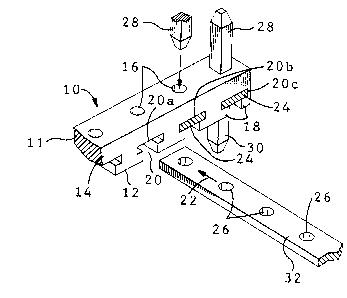
Turning now to the drawings, Figure 1 shows a
schematic perspective view of a presently preferred
embodiment 10 of the electrical connector of this
invention during assembly. As shown in Figure 1, the
connector 10 includes a connector body 11 formed of an
insulating material, and this connector body 11 defines a
lower surface 12 and two parallel side surfaces 14. The
lower surface 12 is intended to be positioned adjacent a
printed circuit board or the like when the connector 10 is
mounted in position. The connector 10 of Figure 1 is a
pin header.
The connector body 11 defines an array of pin
receiving apertures 16 spaced along the length of the
connector body 11. Each of the pin receiving apertures 16
is associated with a respective channel 20 formed in the
connector body. Each of the channels 20 is bounded at its
lower side by a pair of opposed flanges 18. Each of the
channels 20 i8 generally T-shaped in cross section and
opens downwardly at the lower surface 12 and also at each
of the side surfaces 14. Each of the channels 20 defines
a respective loading axis. The arrow 22 is aligned with
the loading axis of one of the channels 20a. In this
embodiment, each of the channels 20 maintains the same
cross sectional shape and dimensions throughout the width
of the connector body 11.
14265CA -6-
13t~ 77
The channels 20 each receive a respective reflowable
element such as a solder element 24. Each of the solder
elements 24 defines a respective opening 26, and the
solder elements 24 are sized to move into the channels 20
along the loading axis 22. Once the solder elements 24
are properly positioned within the channels 20, the
flanges 18 prevent the solder elements 24 from moving
downwardly, toward the lower surface 12. As shown in
Figure 1, the flanges 18 and therefore the channels 20
provide a positive mechanical interlock that prevents the
solder elements 24 from moving in any direction other than
along the loading axis of the respective channel 20.
As shown in Figure 1, after the solder elements 24
are positioned within the channels 20, conductive pins or
posts 28 are passed through the pin receiving apertures 16
and the openings 26. Once positioned in the body 11, the
pins 28 stake the solder elements 24 in place in the
channels 20, thereby positively preventing the solder
elements 24 from moving along the loading axis 22.
From th:is description it should be apparent that the
pins 28 co~perate with the connector body 11 to immobilize
the solder elements 24 in place. The mechanical interlock
between the channels 20 and the solder elements 24
prevents the solder elements 24 from moving in any
direction other than along the loading axis 22. The pins
28 prevent the solder elements 24 from moving along the
14265CA -7-
~3V1E~)7
loading axis 22. Thus, once the pin 28 is inserted in the
pin receiving aperture 16 and the opening 26, there is no
chance for the solder element 24 to beco~e dislodged from
the connector 10.
Figure 1 schematically shows three steps in the
assembly of the connector 10. First, the solder element
24 is moved into the channel 20a along the loading axis
22. At this stage, the solder element 24 is integral with
a solder ribbon 32 stored on a reel (not shown). In the
next step (shown at channel 20b), the solder element 24 is
severed from the solder ribbon 32. In the third step (as
shown at channel 20c), the pin 28 is passed through the
pin receiving aperture 16 and the opening 26 to complete
the assembly. In Figure 1 reference numeral 30 is used to
indicate the printed circuit board connection end of the
pin 28.
In this embodiment, the full width of each of the
solder elements 24 is exposed at each side surface 14 of
the connector 10. With this arrangement, the connector 10
ls well suited for use in infrared reflow systems. In
use, the connector 10 is placed on a support such as a
printed circuit board (not shown), with the ends 30 of the
pins 28 inserted in plated through holes (not shown). The
lower surface 12 functions as a standoff. The solder
elements 24 are then melted, for example by infrared
radiation, and solder flows down the pins 28 to solder the
14265CA -8-
13~18~7
pins 28 in the through holes (not shown). The exposed
ends of the solder element 24 are well positioned to
absorb infrared energy directly from both sides of the
connector 10. Also of importance, the narrow portions of
the T-shaped channels beneath the solder elements 24 allow
solvents to flow through the connector lO after the reflow
operation to wash away the flux commonly used in
soldering.
Figures 2-4 schematically illustrate a second
preferred method for assembling the connector 10. As
shown in Figure 2, the first step is to pull the ribbon 32
of solder into position beneath a punch 40 and to punch
one of the solder elements 24 from the ribbon 32. At this
stage, the ribbon 32 and the resulting solder element 24
are aligned with a selected one of the channels 20d. For
example, the solder ribbon 32 can be made from flux core
solder wire which has been flattened and stored on a reel.
The solder element 24 has a width slightly smaller than
the width of the wide portion of the T-shaped channel 20d.
The solder element 24 is held co-planar and in alignment
with the enlarged portion of the T-shaped channel 2Od. A
pushing mechanism (not shown) then pushes the solder
element 24 along the loading axis 22 to place the solder
element 24 within the channel 20d.
The connector body is then indexed to the position
shown in Figure 3. Figure 3 shows the solder element 24
14265CA -9-
~3~8~7
positioned within the channel 20d and a next solder
element 24 aligned with the channel 20e.
Figure 4 sho~s a third stage in the assembly of the
connector 10, in which the connector 10 has been advanced
so that the solder ribbon 32 is aligned with the channel
20f. In addition, one of the pins 28 has been installed
in the connector 10 by passing it through the pin
receiving aperture 16 and the opening 26. The pin 28
positively retains the solder element 24 within the
channel 20d in all three axes.
The method of Figures 2-4 is especially well suited
for high speed assembly systems. Because the solder
ribbon 32 is pulled rather than pushed, problems
associated with the tendency of a solder ribbon to deform
or wander when pushed at high accelerations are avoided.
For this reason, the embodiment of Figures 2-4 may be
preferred over the embodiments of Figures 1 and 5-7 for
many applications.
Figure 5 shows a schematic representation of a third
preferxed method for assembling the connector 10. In the
method of Figure 5, the solder elements 24 are carried on
a carrier strip 34, and all of the solder elements 24
(four in this example) are simultaneously inserted into
the corresponding channels 20 by moving the carrier strip
34 in the direction shown by the arrows 36. Once all of
the solder elements 24 have been positioned properly in
14265CA -10-
~3018'~7
the channels 20, pins (not shown in Figure 5) are
installed through the pin receiving apertures 16 to stake
the solder elements 24 in place, and the carrier strip 34
is removed. As shown in Figure 5, it is not essential in
all embodiments that the solder elements 24 be provided
with preformed openings 26, and in these cases the pins
may form the desired openings in the solder elements 24
during assembly.
Figures 6 and 7 show steps in a fourth preferred
method for assembling the connector 10. In the method of
Figures 6 and 7, a pair of punch wheels 44 are provided to
punch the openings 26 in the solder ribbon 32, and to
advance the solder ribbon 32 in an indexed manner. A
ribbon feeding finger 42 is provided which is moved in a
four step cycle as shown in Figure 6. In the first step
the ribbon finger 42 moves along the direction of the
arrow 48a to engage the ribbon finger 42 in one of the
openings 26. In the second step the ribbon finger moves
as shown b~ the arrow 48b to pull the solder strip 32 into
the channel 20. Simultaneously, the punch wheels 44 are
indexed so as not to stretch the ribbon 32. In the third
step, the ribbon finger 42 moves along the direction of
the arrow 48c to retract the ribbon finger 42 from the
opening 26. In the fourth step indicated by the arrow
48d, the ribbon finger 42 returns to its original
position. Figure 7 shows the next stage in this assembly
14265CA
13~1~797
method, in which a blade 26 is passed next to the housing
to sever the ribbon 32 and leave a discrete solder element
24 in the channel 20. A conductive pin (not shown) is
then mounted in the housing as described above to
immobilize the solder element 24 in the channel 20.
The method of Figures 6 and 7 is illustra~ed in
connection with a modified form 10' of the connector of
this invention which includes multiple parallel rows of
pins 28. Figures 8-10 are top, bottom and side views,
respectively, of the housing 11 of one of these modified
connectors 10'. Figure 11 is a cross section of the
modified connector 10' taken along line 11-11 of Figure 9.
In the modified connector 10' as shown in Figures 8-11,
the same reference numerals are used as in Figures 1-7 for
corresponding elements. As before, each of the pin
receiving apertures 16 is aligned with a respective
T-shaped channel 20. However, since in this case there
are two rows of pin receiving apertures 16, each of the
channels 20 extends only partly into the connector body
11. Thus, each of the T-shaped channels 20 is closed
ended, as shown in dotted lines in Figure 9 and in cross
section in Figure 11. Any of the assembly methods
described above can be used to insert solder elements 24
in the channels 20. As before, the pins 24 stake the
solder elements 24 in place in the channels 20.
14265CA -12-
~3~8~7
All of the connectors discussed above utilize pins
adapted for insertion into plated through holes, and in
all of the assembly methods discussed above the pins are
inserted into the pin receiving apertures 16 from above
connector body 11. However, this invention is not so
limited and other types of pins can be used. Furthermore,
the pins can be inserted into the apertures 16 either from
above or below connector body 11, depending on the pin
configuration and application.
Figure 12 shows a third preferred embodiment lO" of
the connector of this invention that includes a modified
pin 28'. The pin 28' includes a mounting end 29 adapted
to be surface mounted to a support surface such as a
printed circuit board. The connector lO" is otherwise
similar to the connector lO' of Figures 8-11.
As shown in Figure 12, the connector lO" is assembled
in a manner similar to that described above in connection
with Figure 1. However, in th0 method of Figure 12 the
pin 28' is inserted into the body 11 from below, as shown
at 23. Thus, the upper end of the pin 28' passes first
through the opening 26 in the solder element 24, and then
through the pin receiving aperture 16 of the body 11.
Connector lO" shown in Figure 12 is a dual row
connector with mounting ends 29 of pins 28' of each row of
pins extending laterally toward a respective side surfaces
14 of the housing. For a single row connector, the
14265CA -13-
13~ '7
mounting ends 29 of pins 28' would extend alternately
toward side surfaces 14.
In use, the assembled connector 10" is secured in
placa by positioning the connector 10" in place with the
mounting ends 29 of the pins 28' on respective conductive
pads (not shown). Any suitable means can be used to hold
the connector temporarily in place, such as the
conventional board locks shown in U.S. Patents 4,477,142
(Cooper, et al.), 4,717,219 (Franz, et al.) and 4,679,883
(Assini, et al.). Then the solder elements 24 are heated
to melt the solder elements and cause solder to travel out
of the channels 20, along the pins 28' to the mounting
ends 29 to secure the mounting ends 29 to conductive pads
(not shown) on a printed circuit board (not shown).
Simply by way of example, the following illustrative
dimensions are provided. In this preferred embodiment the
T-shaped channel 20 is 0.070" wide at the wide portion of
the T-shaped channel, and 0.040" wide at tbe narrow
portion of the T-shaped channel 20. In this embodiment
the solder elements 24 are approximately 0.068" wide.
This provides an adequate tolerance to allow easy
insertion of the solder elements 24 into the channels 20.
With these dimensions, the flanges 18 support
approximately 0.014" of the solder elements 24 on each
side of the channel.
14265CA -14-
~3(~
In this example, the cross sectional dimensions of
the pin 28 are 0.025 inch by 0.025 inch, and each of the
openings 26 is 0.027 inch in diameter. This geometry has
been found to provide adequate contact between the solder
preform 24 and the pin 28 to ensure that solder will flow
along the pin 28 during the reflow operation to form a
reliable solder bond between the pin and a plated through
hole of a printed circuit board. The thickness of the
solder preform 24 is 0.017 inches, and the height of the
wide portion of the T-shaped channel 20 (measured along
the pin 28) is 0.020 inches. The overall height of the
channel 20 i8 O. 035 inches.
The housing 11 can be made of any suitable insulating
material. One suitable material is the liquid crystal
polymer thermoplastic sold under the tradename Vectra
A-130 (Celanese Corporation). The pin 28 can be formed of
any suitable solder-wettable conductive material of
adequate strength, of solid or formed construction.
Although a square cross section has been shown, circular
or other 6hapes may also be used. The pin should
preferably be sized to form a friction fit with the
housing in the pin receiving aperture 16.
The solder element 24 can be formed of any suitable
solder alloy, such as a 60/40 or 63/37 tin-lead alloy. A
flux such as a mildly activated rosin may be included in
the element 24, or alternately flux may be added later.
14265CA -15-
13(~18~7
Of course, this invenkion is not limited to use with
headers as illustrated in the drawings, but can be used
with a wide variety of electrical connectors, including a
wide range of connectors for both surface mount and
through hole mount applications, connectors with
integrally mounted electrical components such as
transformers, edge connectors, socket connectors, and the
like. Also, this invention is not limited to use with
T-shaped channels, but can also be used with L-shaped
channels having only a single flange 18.
Solder elements have been used above as examples of
suitable reflowable elements, and a~ pointed out above, a
variety of solders can be used. Depending upon the
application, other metals and conductive adhesives can be
used for a reflowable element, as long as the chosen
material (1) has sufficient rigidity to be retained by the
channel and pin structure described above, and (2) can be
caused to reflow down the pin to form an electrical
connection. Of course, this invention is not limited to
use with square reflowable elements. Rather a wide
variety of shapes can be used, including discs, washers
and tori.
Conventional materials can be used for the connector
housing, the pins, and the solder elements, and this
invention is not restricted to the particular materials
described above. Those skilled in the art are well versed
14265CA -16-
13~)113~'7
in the selection of suitable materials, depending upon the
temperature and structural requirements of the particular
application. Of course, it should be understood that a
wide range of changes and modifications can be made to the
preferred embodiments described above. It is therefore
intended that the foregoing description be regarded as
illustrative rather than limiting, and that it be
understood that it is the following claims, including all
equivalents, which are intended to define the scope of
this invention.
14265CA -17-