Note : Les descriptions sont présentées dans la langue officielle dans laquelle elles ont été soumises.
~3~2477
RCA 82,340
DEVICE AND METHOD
FOR MONITORING A
LIGHT EMITTING DEVICE
The invention relates to a device and method for
~onitoring the output of surface emitting devices.
Back~round of the Invention
One type of construction of a surfac0 emitting device use6
a grating surface in a large optical cavity index-guided
laser. These devices may be formed on a single s~trate
to for~ an array of devices which emit a radiation pattern
which is typically about perpendicular to the grating
surface. The output of these arrays are typically
monitored by insertin~ a detecting device, such as an array
of charge-coupled devices in this radiation pattern. This
monitoring is initially required to adjust dri.ve currents
to produce a desired ar field pattern and further
monitoring is typically necessary to adjust the drive
currents to compensate for changes in ambient conditions
and to compensate for the aging of the device. Thçrefore,
it would be desirable to have a light emitting device and a
method of monitorins the device in which the monitoring
eguipment is not inserted i~ the primary radiation pattern.
Summary of the Invention
A surface emitting device comprises a substrate
having a large optical cavity region overlying the
substrate. The large optical cavity region has both
exposed and unexposed areas. Overlying the unexposed areas
are an active region and a capping layer overlying the
active region. Overlying the exposed area of the large
optical cavity region is a grating region formed ~f a first
grating region having a first period and a second region
having a period different frum the first region.
The invention also includes an array of surface
emitting devices. This array has a ~ubstrate, a large
optical cavity region overlying the substrate, a first
active region overlying a irst portion of tha cavity
~3~ LY~7
- 2 - RCA 82,340
region and a second active region overlying a second portion of the
cavity region. Capping layers overlie the active regions an~ the device
includes a means for electrically contacting the substrate and capping
layers. A first gratiny region overlies the cavity region and the
grating region is formed of a plurality of substantially equally spaced
elem~nts. A second grating region also overlies the cavity region which
has a plurality of elements which have a spacing different from said
first grating region.
Finally, the invention includes a ~ethod of monitoring the
light emitting device which includes formlng a surface emittin~ device
with first and second gratings with the grating having different
periods. Current is applied to the device such that radiation is
emitted from the grating and the output is detected frcm the second
yrating such that the current to the device is adjusted based on the
output of the s~cond grating.
Brief Description of the Drawinq
FIG. 1 is an isometric view of an array in accorlance with the
invention;
FIG. 2 is a cross-sectional view of a laser used in FIG. l;
FIG. 3 is a cross-sectional view of a first embodLment of a
yrating used in the array of FIG. 1; and
FIG. 4 is a cross-sectional view of a second embodim;nt of a
yrdtLng used Ln the array of FIG. 1.
etailed DescriPkion of the Preferred Embcdinents
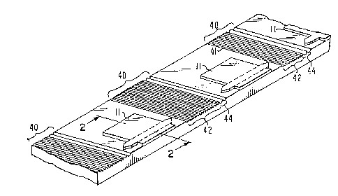
In FIG. 1 a surface emltting array lO compris s a plurality of
semiconductor diode sections 11. As shown in FIG. 2, ~hese diode
sections 11 comprise a substrate 12 having a first cladding region 14
thereon. A large optical cavity region 16 overlies the first cladding
region 14, an active region 18 overlies the large optical cavity region
30 16, a second cladding region 20 cverlies the active region 18, and a
capping layer 22 cverlies the second cladding r2gion 20. A means for
electrically contacting the device comprises a first electrical contact
30 which overlies the surface of the substrate 12, opposite the first
cladding region 14 and a second electrical contact 32 which overlies the
35 capping layer 22. In the array of FIG. 1 the diode sections 11 are
connected togeth~r by the cavity region 16 which extends between the
diode sections 11 and overlying the cavity region 16 between the diode
sections is a grating region 40. The gratLng r0gion 40 typically is
co~posed of a plurality of sukstantially parallel elements
.1 i.,
2~177
-3- PATENTS
RCA 82,340
41 ~ormed on the surface of the cavity region 16. As shown
in FIG. 3 the grating region 40 comprises a first output
gratin~ 42 with the gratings having a substantially equal
period 43 and a second monitor grating 44 with each monitor
gratinq period 45 being different than the output grating
period 43. It should be understood the output and monitor
gratings 42 and 44 respectively may be adjacent as in FIG.
3. Alternatively, other grating systems m~y be used as in
FIG. 4 in which a portion of the output grating 42 is
positioned on the monitor grating 44 such that output
grating 42 is a modulation on the monitor grating 44.
The substrate 12 is typically composed of N-type
GaAs about 250 micrometers (~m) thick and having a first
~ajor surface parallel to or slightly misoriented from the
(100) cyrstallographic plane. The first cladding region 14
is typically about 1.26 ~m thick and is typically composed
of N-type AlxGa1 xAs where x is generally between about 0.2
and 0.4 and is typically about 0.27~ . The cavity region
16 is typically between about 0.25 and 0.60 ~Im th:icls and is
typically composed of N-type AlxGal_xAs where x is
generally between about .15 and .25 and is typically about
0.18. The active region 18 is typically about 0.0~ ~m
thick and is typically composed of N-type AlxGal xAs where
x is typically about 0.06. The second cladding region 20
is typically between about 1.2 and 1.7 ~m thick and is
typically composed of AlxGa1_xAs where x is about 0.4. The
first electrical contact 30 is preferably composed of
s~quentially deposited germanium, gold nickel and gold
layers. The second electrical contact 32 is preferably
composed of titam um, platlnum and gold layers which are
sequentially deposited onto a Zn or Cd diffused surface.
It should be understood that other surface emitting device
structures which utilize a surface g.rating are equally
applicable to the present invention.
3~ The array 10 may be fabricated using standard
liguid phase epitaxy techniques to deposit the layers and
regions. Suitable liquid phase epit~xy technigues have
been disclosed by Lockwood et al. in U.S. Patent No.
~3~7~
_4~ PAl~NTS
RC~ 82, 340
3,753,801, issued August 21, 1978. Photore~ist is
then fonned on the diode sections 11 and t:h@ ~econd
electrical contact 32 is th~n removed by ion milling
outside the diode sections 11. The capping layer Z2,
5 second cladding region 20 and active reglon 18 are then
removed outside the diode fiections 11 typically by a
chemical removal such as by a buffered HF 60lution and
~I2S04:EI202:E~20. The grating region i~ typically fonned by
first forming the output grating 42 by forming a p~riodic
10 grating using standard holographic and etchir~g tecbni~u~a.
Alternatively, the grating may be for~ed by ion ~illing.
Typically ~he period of the ou~put grating 43 i~ about 240
nanometer6 (nm~ It should be un~er~tood that it may be
desirable to first form the monitor grating 44 to form
other configurations such as shown in FIG. 4. The monitor
grating 44 is formed by the same t~chni~ues to have a
periodic length different than th~ output ~rating so that
the angle of the optical axis emitted radiation from the
monitor grating 44 relative to the plane of the layer~ ia
different than th~ angle of the optical a~is of the e~itted
radiation from the output grating 42. Preferably the
periodic length of the monitor grating 44 is larger than
the periodic length of the output grating 42. Typically~
the angle of output ~ fro~ the monitor grati~g mea~ured
from the surface will be about
COS 1 ~ ( neA -Amc )/ ( nOA ) :1
where A is the wavelength of radiation, mc is an integer
con~tant (1, 2, 3...), A is the period of the monitor
grating, ne is the effective inde~ of refraction in the
large optical cavity region and nO is the effectiv~ inde~
: of refraction in air. ~ may be about 375 nm such that
will be about ln.
In operation, a bias voltage of the proper
polaxity i~ appli~d to the first and second electrical
contacts 30 and 32 respectively, producing radiation i~ the
active region 18. This radiation i~ emitted in part by the
output grating 42. The angle of the optical axis of
emitted radiation is typically perpendicular ~o the plane
.
~3~æ~
_5_ PATENTS
RCh 82,340
of the layers. A portion of the radiation is also emitted
from the monitor gratin~. A detecting de~ice such as an
array of CCD detectors, as is well ~nown in the art, is
positioned to receive radiation from the monitor grating
and the plane of the detecting devi.ce is t~pically
perpendicular to the optical axis of emitted radiation from
the monitor grating. The detectinc~ device transmits
electrical signals to a viewiny device, which depicts the
output from the monitor grating. This output from the
monitor grating 44 will have a unic~e relationship with the
output of the output grating 42 since each is subject to
the same interference conditions. For example, in ~ome
device configurati~ns a single lobe from the ou~put of the
monitor grating 44 would correspond to a single lobe from
the output grating. It should be understood that this
unique rel~tionship is not necessarily the same pattern for
the output and monitor gratings 42 and 44 respectively, and
is therefore typically determined experimentally through
trial and error by first monitoring outputs from both
gratings. Therefore, the current supplied to the device
will be adjusted to initially desired dri~e currents by
observing the output of the monitor grating 44 and will be
subse~uently adjusted to adjust for compensation of aging
or changes in a~bient conditions.