Sélection de la langue

Search

Sommaire du brevet 1302497 

Énoncé de désistement de responsabilité concernant l'information provenant de tiers

Une partie des informations de ce site Web a été fournie par des sources externes. Le gouvernement du Canada n'assume aucune responsabilité concernant la précision, l'actualité ou la fiabilité des informations fournies par les sources externes. Les utilisateurs qui désirent employer cette information devraient consulter directement la source des informations. Le contenu fourni par les sources externes n'est pas assujetti aux exigences sur les langues officielles, la protection des renseignements personnels et l'accessibilité.

Disponibilité de l'Abrégé et des Revendications

L'apparition de différences dans le texte et l'image des Revendications et de l'Abrégé dépend du moment auquel le document est publié. Les textes des Revendications et de l'Abrégé sont affichés :

  • lorsque la demande peut être examinée par le public;
  • lorsque le brevet est émis (délivrance).
(12) Brevet: (11) CA 1302497
(21) Numéro de la demande: 1302497
(54) Titre français: INTERRUPTEUR DE COURANT ALTERNATIF
(54) Titre anglais: AC CURRENT SWITCH
Statut: Périmé et au-delà du délai pour l’annulation
Données bibliographiques
(51) Classification internationale des brevets (CIB):
  • H03K 17/687 (2006.01)
  • H03K 17/082 (2006.01)
  • H03K 17/74 (2006.01)
(72) Inventeurs :
  • JONES, THAD M. (Etats-Unis d'Amérique)
(73) Titulaires :
  • THAD M. JONES
(71) Demandeurs :
(74) Agent: BORDEN LADNER GERVAIS LLP
(74) Co-agent:
(45) Délivré: 1992-06-02
(22) Date de dépôt: 1989-07-25
Licence disponible: S.O.
Cédé au domaine public: S.O.
(25) Langue des documents déposés: Anglais

Traité de coopération en matière de brevets (PCT): Non

(30) Données de priorité de la demande:
Numéro de la demande Pays / territoire Date
255,964 (Etats-Unis d'Amérique) 1988-10-11

Abrégés

Abrégé anglais


AC CURRENT SWITCH
Abstract of the Disclosure
A current switch which emulates a thyristor by
using enhancement mode field effect transistors. A
center tapped current transformer and a push-pull
field effect transistor arrangement eliminates the
need for either rectifier diodes or a full wave bridge
connected to the current transformer.

Revendications

Note : Les revendications sont présentées dans la langue officielle dans laquelle elles ont été soumises.


THE EMBODIMENTS OF THE INVENTION IN WHICH AN EXCLUSIVE
PROPERTY OR PRIVILEGE IS CLAIMED ARE DEFINED AS FOLLOWS:
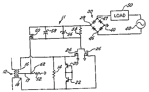
1. A device for switching a first electrical
current flowing in a first conductor responsive to a
second electrical current flowing in a second
conductor, said device comprising,
means for switching said first current, said
means having a conductive and nonconductive mode,
means connected to said switching means and
operatively associated with said second conductor
for sensing said second current, means connected
to said switching means for latching said
switching means in one of said conductive and
non-conductive modes, a voltage source connected
to said latching means, said sensing means
including a transformer having a center tapped
secondary winding and a single turn primary
winding operatively associated with said second
conductor,
said switching means including a first field
effect transistor (FET) having a gate terminal,
a drain terminal, and a source terminal, said
gate terminal being connected to said transformer
secondary terminal, said drain terminal connected
to said latching means,
said latching means including a second field
effect transistor (FET) having a gate terminal,
a drain terminal, and a source terminal, said

second FET gate terminal being connected to said
first FET drain terminal, said latching means
further including a capacitive member and a
voltage limiting member operatively associated
with said second FET, said latching means being
electrically connected to said voltage source.
2. The device of Claim 1 wherein said latching
means includes a third field effect
transistor having a gate terminal, a drain
terminal and a source terminal, said third FET
source terminal being connected to said second
FET gate terminal, said second FET drain terminal
being connected to said third mentioned gate
terminal, said third mentioned drain terminal
being connected to said voltage source, said
voltage limiting means connected between said
third FET drain terminal and said third FET gate
terminal wherein said second FET and said third
FET are in a mutually biasing relationship.
3. The device of Claim 2 wherein said first FET
begins conducting and interrupts the mutually biasing
relationship of said second and third FETs to switch
said device from said conductive mode to said
nonconductive mode to interrupt said first current
when said second current rises above a threshold level
of said first FET.

4. The device of Claim 1 wherein said
capacitive member and said voltage limiting member are
connected in parallel between the drain terminal and
gate terminal of said second FET, said second source
terminal being connected to a center terminal of said
transformer secondary winding.
5. The device of Claim 1 wherein said second
FET conducts as the first FET begins conducting,
whereby said first FET and said second FET are
mutually biasing to switch said device from said
nonconductive mode to a conductive mode to establish
said first current when said second current rises
above a threshold level of said first FET.
6. A device for switching a first electrical
current flowing in a first conductor responsive to a
second electrical current flowing in a second
conductor, said device comprising,
means for switching said first current, said
means having a conductive and nonconductive
mode,
means connected to said switching means and
operatively associated with said second conductor
for sensing said second current, means connected
to said switching means for latching said
switching means in one of said conductive and
non-conductive modes, a voltage source connected
to said latching means, said sensing means
11

including a transformer having a center tapped
secondary winding and a single turn primary
winding operatively associated with said second
conductor,
said switching means including a first field
effect transistor (FET) having a gate terminal,
a drain terminal, and a source terminal, said
gate terminal being connected to said transformer
secondary terminal, said drain terminal connected
to said latching means,
said latching means, including a second
field effect transistor (FET) having a gate
terminal, a drain terminal and a source terminal,
said second FET gate terminal being connected to
said first FET drain terminal, said latching
means further including a capacitive member and
a voltage limiting member operatively associated
with said second mentioned FET,
said latching means being electrically
connected to said voltage source, wherein said
latching means includes a third field effect
transistor (FET) having a gate terminal, a drain
terminal and a source terminal, said third FET
source terminal being connected to said second
FET gate terminal, said second FET drain terminal
being connected to said third mentioned gate
terminal, said third FET drain terminal being
12

connected to said voltage source,
said voltage limiting means is connected
between said third FET drain terminal and said
third FET gate terminal wherein said second FET
and said third FET are in a mutually biasing
relationship.
7. The device of Claim 6 wherein said first FET
begins conducting and interrupts the mutually biasing
relationship of said second and third FETs to switch
said device from said conductive when said second
current rising above a threshold level of said first
FET mode to said non-conductive mode to interrupt said
first current.
8. A device for switching a first electrical
current flowing in a first conductor responsive to a
second electrical current flowing in a second
conductor, said device comprising,
means for switching said first current, said
means having a conductive and nonconductive
mode,
means connected to said switching means and
operatively associated with said second conductor
for sensing said second current, means connected
to said switching means for latching said
switching means in one of said conductive and
non-conductive modes, a voltage source connected
to said latching means, said sensing means
13

including a transformer having a center tapped
secondary winding and a single turn primary
winding operatively associated with said second
conductor,
said switching means including a first field
effect transistor (FET) having a gate terminal,
a drain terminal, and a source terminal, said
gate terminal being connected to said transformer
secondary terminal, said drain terminal connected
to said latching means,
said latching means including a second field
effect transistor (FET) having a gate terminal,
a drain terminal and a source terminal, said
second FET gate terminal being connected to said
first FET drain terminal, said latching means
further including a capacitive member and a
voltage limiting member operatively associated
with said second FET, said latching means being
electrically connected to said voltage source,
wherein said capacitive member and said voltage
limiting member are connected in parallel between
the drain terminal and gate terminal of said
second FET, said second mentioned source terminal
being connected to a center terminal of said
chance former secondary winding.
9. The device of Claim 8 wherein said first FET
begins conducting and causes said second FET to
14

conduct, thereby said first FET and said second FET
are mutually biasing to switch said device from said
non-conductive mode to a conductive mode to establish
said first current when said second current rising
above a threshold level of said first FET.

Description

Note : Les descriptions sont présentées dans la langue officielle dans laquelle elles ont été soumises.


~3~
AC CURP~ENT SWITCH
Su_mary ~I t-e Irv~ on
This invention relates to current switches and
has specific reference to an AC current switch having
increased sensitivity.
Heretofore, current switches typically used a
threshold current of about .5 amps and employcd
bipolar transistors for switchiny. One problem
associated with the prior current switches using
bipolar transistors is that any attempted lncrease in
the threshold ~ensitivlty of the switch results in a
temperature rise in the circuit thereby requiring a
~O larger transformer which increases the switch cost and
lowers its efficiency.
The current switch of this invention eliminates
the problems experienced with bipolar transistor
current switches by connecting a pair of mode
enhancement field effect transistors so as to emulate
a thyristor thereby increasing switch sensitivity
without an excessive temperature increase. Further,
by implementing a center tapped transformer with a
push-pull field effect transi~tor configuration, the
need for either rectifier diodes or a full wave bridge
rectifier i8 eliminated, thereby reducing the numh~r
of swltch parts.
Accordingly, it is an object of this invention to
provide for a current switch having an increased

sensitivity.
Another object of this invention i5 to provlde
for a current switch ha~ing a reduced part count.
Other objects of this invention will become
apparent upon a reading of the ~ollowing description.
B~ ef Descri~t,~ ~t t ~r~-~n~8
Fi~. 1 is a schematical representation of the
switch of this invention which has a normally closed
configuration.
Fig. 2 is a schematical representation of a
second embodiment of the switch which has a normally
open configuration.
Descri~ on of the Preferred_Embodiments
The preferred embodiments herein disclosed are
not intended to be exhaustive or to limit the
application to the precise forms disclosed. Rather,
they are chosen and described 50 that others skilled
in the art may utilize their teachings.
Fig. 1 illustrates the switch 10 of this
invention in a normally closed configuration. Switch
10 includes a center tapped transformer 12 which has
a resistor 14 connected across secondary terminals 16
and 18. The transformer secondary center terminal 17
is connected to ground. A pair of NPN transistors 20,
22 having common base and collector leads are
connected by their emitter leads across secondary
terminals 16 and 18 as illustrated in Fig. 1. The

~ 3!~t ;~
gate of N--channel enhan~sment mode field effect
transistor (FET) 24 ia connected to terminal 1~ with
the source term.inal of FET 24 connected to ground. A
resistor 25 is con~ect2d between the drain terminal of
FET 2~ and the positive termin~1 :28 of bridge
rectifier 30. The gate of N-channel enhancement mode
F~T 32 is connected to terminal 18 of the secondary
winding of transformer 12. The source terminal of FET
32 is connected to ground. The drain terminal of FET
~0 32 is connected to the source terminal of FET 34 which
has its drain terminal connected to the positive
termlnal 23 oE rectifier bridge 30.
~ xener diode 36 is connected between the drain
and gate terminals of FET 34 with its anode connected
to -the drain. A resistor 38 is connected across zener
diode 36. The drain terminal of FET 40 is connected
to the common connection of zener diode 36, resistor
3e and the gate terminal of FET 34. The ~ate of FET
40 is connected to the aource terminals of FETs 24 and
32. ~ capacitor 42 is connected between the gate of
FET 4Q and ground.
The negative output terminal 44 of bridge
rectifier 30 is connected to ground. Input terminal
46 of rectifier 30 ia connected to one side of ~C
source 48, with the other side of source 48 connected
to one side of a load 50. Input terminal 47 of
rectifier 30 is connected to the other side of load

.
It should be understood that the primary winding
of transformer 12 is preferably a one turn wlnding
used to sense current flowing through a conductor.
In operation, the current transformer 12 senses
the current through a conductor to be monitored,
typically ground. Current transformer 12 provides an
open circuit voltage which i8 non-linearly
proportional to the current flowing through the
primary and the material and geometry of the core.
Resistor 14 determines the sensitivity of switch 10 by
compensatin~ for variations ln the core material of
transform0r 12 and N-channel FETs 24, 32.
NPN Transistors 20, 22 are included and
configured to act as a low lea~age current zener diode
for the protection of FETs 24, 32 from excessive
voltage overload conditions.
Switch 10 of Fig. 1 operates in the following
manner. Initially, one must assume that a sinusoidal
current is sensed by transformer 12 which causes a
transformer secondary voltage peak value less than the
threshold vcltage of N-channel FÆTs 24, 32. Further,
as~ume that the bridge rectifier 30 is producing a
positive voltage at terminal 28. A charging current
flows from terminal 28 through resistor 26 to charge
capacitor 42. N-channel FET 40 begins to conduct upon
capacitor 42 reaching the FET's threshold voltage.

~3~ 7
Current through resistQr 38, caused by FET 40
conducting, creates a voltage drop across the reaistor
38. P-channel FET 34 begins condu&ting upon the
voltage drop across resistor 38 re~aching FET's
threshold voltage. Upon FET 3~ conducting, the
char~ing current of capacitor 42 is increased which
further increases the conduc~ion of E'ET 40. Thia
increase in conduction continues until FET's 34 and 40
reach saturation. Current flow for load 50 is flowing
through bridge rectifier 30, zener diode 36 and N-
channel F~T 40. Zener diode 36 is included to protect
th~ gate of FET 34. Therefore, switch 10 is latched
closed to allow current flow through a load such a~ an
indicator lamp.
As current sens0d by the primary terminal of
transformer 12 rises above the threshold voltages of
FETs 24 and 32 (such as upon occurrence of a ground
fault condition) the peak value of the transformer's
secondary terminals 16, 18 to center tap voltage
instantaneously exceeds -the threshold voltage of N-
channel FET 24 during the positive half cycle and FET
32 during the negative half cycle 32. This causes
either FET 24 or 32 to momentarily conduct thereby
preventing the charging of capacitor 42~ Momentary
diaruption of the chargin~ current to capacitor 42
prevents it from reaching the threshold voltage of FET
40.

~3~
The R--C network of resistor 26 and capacitor 42
cause~ the gate voltage of FET 24 and FET 32 to la~
behind the OlltpUt voltage oP bridge rectifier 30.
This effect combined with the momentary disruption of
the capacitor's charge current prevents switch 10 from
staying closed and the switch 10 is thereby triggered
open to prevent current flow through load 50.
Fig. 2 illustrates a normally open embodiment oP
switch 10. A common numbering system is employed
between Figs. 1 and ~ wherein like numbered components
indicates a similar component and function.
Switch 11 of Fig. 2 includes a transformer 1~,
resistor 14, transistors 20, 22 and FETs 24 and 30
interconnected identical to switch 10 described above
and depicted in Fig. 1. A resistor 52 is connected
between transformer secondary terminal 1~ and ground.
A resistor 54 is connected between the common drain
leads of FETs 24, 26 and to terminal 28 of bridge
rectifier 30. Z0ner diode 56 is connected across
resistor 54 with its cathode electrically connected to
rectifier terminal 28. A capacitor 5~ is connected
across diode 56 and also across the drain and gate
leads of P-channel FET 60. The source lead of FET 60
is connected to junction 62 formed between resistor 52
and transformer ~econdary terminal 17.
In operation, with the transPormer secondary
voltage below the threshold voltage of N-channel FETs

~J'2~
24, ~6 switch 1l is in its open state and no current
i5 flowing through load 50. Upon the transformer
secondary voltage having a pea~ voltage exceeding the
threshold ~oltage of FET 24 for a posi-tive half cycle
and of FET 26 during a negative half cycle the
instantaneous gate voltage of Fh'T 24 or ~ET 26 exceeds
its threshold voltage and the FET begins to conduct.
Upon conduction of FET 24, (or FET 26 if the
transformer secondary voltage is a negative peak
value) a current path from source 48 through load 50,
rectifier 30 and resistor 54 is established. The
voltage drop across resistor 54 creater1 by current
through the re~istor begins to charge capacitor 58.
FET 60 begins to concluct upon the voltaye across
capacitor 58 reaching the FET 60 threshold voltage.
As FET 60 conducts a voltage drop across resistor 52
is created which increases the gate voltage at FET's
24 and 26. Thi5 increase in voltage continues until
the saturation level of ~ET' 5 24 and 26 is attained~
The charge stored in capacitor 5B en~ures switch
conduction during the power line half-cycle.
Normally open switch lO of Fig 2 essentially
consists of the N-channel FETs 24 and 25, and the P-
channel FET 60. In the normally closed embodiment, P-
channel FET 60 is replaced by N-channel FET 40 and P-
channel FET 34. The voltage drop o~ switch ll
approximates the voltage of ~ener diode 56 in the

13q:~Z~
normally open embodiment of Fig. 2 or zener diode 36
in the normally olosed embodiment of Pig 1.
Therefore, both embodiments of the switch (10 and 11~
depicted abuve require no external volta0e souroe but
merely use a small amount of voltage from a source
being monitored.
It should be understood that the invention i~ not
li.mited to the precise cletails above but may be
monitored within the scope of the appended claims.

Dessin représentatif
Une figure unique qui représente un dessin illustrant l'invention.
États administratifs

2024-08-01 : Dans le cadre de la transition vers les Brevets de nouvelle génération (BNG), la base de données sur les brevets canadiens (BDBC) contient désormais un Historique d'événement plus détaillé, qui reproduit le Journal des événements de notre nouvelle solution interne.

Veuillez noter que les événements débutant par « Inactive : » se réfèrent à des événements qui ne sont plus utilisés dans notre nouvelle solution interne.

Pour une meilleure compréhension de l'état de la demande ou brevet qui figure sur cette page, la rubrique Mise en garde , et les descriptions de Brevet , Historique d'événement , Taxes périodiques et Historique des paiements devraient être consultées.

Historique d'événement

Description Date
Inactive : CIB de MCD 2006-03-11
Le délai pour l'annulation est expiré 1997-06-02
Lettre envoyée 1996-06-03
Accordé par délivrance 1992-06-02

Historique d'abandonnement

Il n'y a pas d'historique d'abandonnement

Titulaires au dossier

Les titulaires actuels et antérieures au dossier sont affichés en ordre alphabétique.

Titulaires actuels au dossier
THAD M. JONES
Titulaires antérieures au dossier
S.O.
Les propriétaires antérieurs qui ne figurent pas dans la liste des « Propriétaires au dossier » apparaîtront dans d'autres documents au dossier.
Documents

Pour visionner les fichiers sélectionnés, entrer le code reCAPTCHA :


Pour visualiser une image, cliquer sur un lien dans la colonne description du document. Pour télécharger l'image (les images), cliquer l'une ou plusieurs cases à cocher dans la première colonne et ensuite cliquer sur le bouton "Télécharger sélection en format PDF (archive Zip)" ou le bouton "Télécharger sélection (en un fichier PDF fusionné)".

Liste des documents de brevet publiés et non publiés sur la BDBC .

Si vous avez des difficultés à accéder au contenu, veuillez communiquer avec le Centre de services à la clientèle au 1-866-997-1936, ou envoyer un courriel au Centre de service à la clientèle de l'OPIC.


Description du
Document 
Date
(aaaa-mm-jj) 
Nombre de pages   Taille de l'image (Ko) 
Abrégé 1993-10-30 1 11
Revendications 1993-10-30 7 204
Dessins 1993-10-30 1 27
Dessins représentatifs 2003-03-11 1 14
Description 1993-10-30 8 252
Taxes 1995-03-19 1 35
Taxes 1994-05-19 1 51