Note : Les descriptions sont présentées dans la langue officielle dans laquelle elles ont été soumises.
~3~ 5~3
Magnetron feeding apparatus and method of controlling
the same
The present invention generally relates to improvements
in a high-frequency heating apparatus for heating food,
liquid or the like by so-called dielectric heating, and,
more particularly, to a magnetron feeding (supply)
apparatus, and a method of controlling such apparatus,
which method is adapted to effect operation of a magnetron
by means of an inverter circuit using a semiconductor
switch and a high-tension transformer.
To enable the prior art to be described with the aid
of a diagram, the figures of the drawings will first be
listed.
Fig. l is a block diagram of a conventional magnetron
feeding apparatus;
Fig. 2 is a conceptional diagram of a magnetron feeding
apparatus according to an embodiment of the present
invention;
Fig. 3 is a block diagram of a first embodiment of an
output voltage detecting portion;
Fig. 4 is a block diagram of a second embodiment of an
output voltage detecting portion;
Fig. 5 is a block diagram of a first embodiment of a
power supply portion;
~'.'-' ~
~3~ 3
-- 2
Fig. 6 is a block diagram of a second embodiment of a
power supply portion;
Fig. 7 is a block diagram oE a Eirst embodiment of an
input current detecting portion;
Fig~ 8 is a block diagram of a second embodiment of an
input current detecting portion;
Fig. 9 shows a slmple equiva]ent circuit of a
magnetron;
Fig. 10 shows a charaeteristic graph of a magnetron;
Fig. 11 shows a characteristic graph of a magnetron
feeding apparatus;
Fig. 12 is a bloek diagram of a first emhodiment of a
power controlling portion
Fig. 13 shows a start eharacteristie graph of a
magnetron feeding apparatus;
Fig. 14 is a block diagram of a first referenee signal
generating eireuit;
Fig. 15 is a block diagram of a first gradual
inereasing eircuit;
Fig. 16 is a block diagram of a power controlling
portion
Fig. 17 is a characteristic graph thereof;
Fig. 1~3 is a block diagram of a second embodiment of a
power controlling portion;
Fig. 19 is a block diagram of a third embodiment of a
power controlling portion;
Fig. 20 is a characteristic graph of a magnetron
feeding apparatus;
Fig. 21 is a diagram of another conventional
construction of a magnetron feeding apparatus;
Fig. 22 is a block diagram of a magnetron feeding
apparatus when a power controlling operation is performed
by a software processing operation;
Fig. 23 is a conceptual diagram of this operation; and
Figs. 24 - 26 are each a flow chart of embodiments of
a software processing operation.
--` 13~25~L3
-- 3
Generally, a magnetron feeding apparatus such as shown
in Fig. 1 is adapted to convert a DC current 2 from a power
supply portion 1 into high-fre~uency power 5 by means of
an inverter circuit 4 using a semiconductor switch 3, such
as a transistor of the like, and furthermore to convert
the power 5 into high-tension power 7 by means of a high-
tension transformer 6 to feed the power to a magnetron 8.
A method of controlling the power comprises the steps
of detecting the input current from a commercial power
supply 9 by an input current detector 10, generating
difference information 12 between its value and that of a
reference signal 11 by means of an error amplification
circuit 13. A driving circuit 14 generates a driving
pulse 15 corresponding to this difference information 12
to turn on or off the semiconductor switch 3, so that the
input current is controlled to a predetermined value.
However, as most of the power fed to the magnetron 8
is consumed by a heater 8H hefore the magnetron 8 starts
oscillation, the initial power will be approximately one-
seventh of the power at steady-state when the magnetron
8 is oscillating.
Thus, if the input current is controlled to the pre-
determined value in the period before the magnetron 8
starts oscillation, excessive power is applied to the
heater 8H, and also an excessive voltage is applied
between the anode 8A and the cathode 8K, resulting in the
life of the magnetron 8 being shortened because of dis-
charging, deteriorated insulation or the like.
Before the magnetron 8 starts oscillating the reference
signal 11 is set to a value smaller than at steady-state
so as to produce a smaller input current appropriate to
the heater operation. ~y means of a timer 16~ the
reference signal 11 is switched to the steady-state
value after the lapse of sufficient time for the magnetron
~L3~25~3
,
-- 4
8 to start oscillation.
As the time required for the oscillatlon to be started
is two seconds when the magnetron 8 is kept warm, and four
seconds when it is cold, the timer 16 is set for five
seconds for safety.
As the magnetron 8 has no output for five seconds,
there is a wasted time of 5-2=3 seconds when the magnetron
8 is kept warm, and of 5-4=1 second when the magnetron 8
is cold. As a result the high-speed cooking capability
that is characteristic of an electronic range is
deteriorated.
Accordingly, an essential object of the present
invention is to provide a magnetron feeding apparatus that
is capable of controlling the output voltage of the high-
tension transformer and the input current to the invertercircuit.
Another important object of the present invention is
to provide apparatus that is capable of reaching the
oscillating condition of the magnetron within a shorter
time.
A further object of the present invention is to
provide apparatus of the above-described type in which a
controlling operation is effected so that the input current
can reach a given value so that the starting operation can
be achieved without a waste of time, and also that the
oscillating condition can be stably continued.
To this end, the invention consists of a magnetron
feeding apparatus comprising a power-supply portion for
supplying a DC current, an inverter circuit for converting
the DC current into high-frequency power through a
switching operation of a semiconductor switch, a high-
tension transformer for converting the high-frequency
power into high-tension power to be applied to a
magnetron, an output voltage detection portion for
~ ~3()25~3
-- 5 --
detecting the output voltage of the high-tension
transformer, an input current detecting portion for
detecting input current into the inverter circuit, a power
controlling means for controlling the switching operation
of the semiconductor switch by means of the output voltage
information of the output voltage detecting portion and
the input current information of the input current
detecting portion.
The invention also consists of a method of controlling
such apparatus.
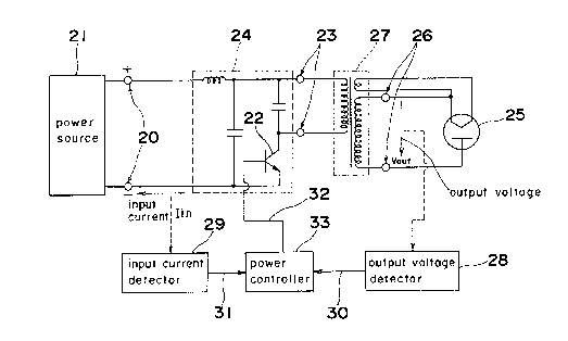
Referring now to the drawings, there is shown in Fig.
2 a magnetron feeding apparatus that includes a power
supply portion 21 for supplying DC current 20, an inverter
circuit 24 which switches at high frequency the DC power
supply 20 by means of a semiconductor switch 22 to generate
high-frequency power 23. A high-tension transformer 27
converts the power 23 into the high-tension power 26
necessary for the operation of a magnetron 25. An output
voltage detector 28 detects the output voltage Vout
of the transformer 27. An input current detector 29
detects the input current Iin into the inverter circuit
24. A power control portion 33 controls the switching
operation of an inverter circuit 24 by outputting driving
pulses 32 which turn on or off the semiconductor switch
22, based on information 30 from the detector 28 and the
information 31 from the detector 29.
Fig. 3 is a diagram of a first embodiment of an output
voltage detector 28'. A separate detection winding 34 is
provided on the output (secondary) side of the high-
tension transformer 27', with the output of such winding
being supplied as information 30' through a first
rectification circuit 35. The information 30' corresponds
to the output voltage Vout.
Fig. 4 is a diagram of a second embodiment of an
output voltage detector 28''. A detecting winding 36 is
formed from a portion of the main secondary winding of a
high-tension transformer 27'', with the output of the
winding 36 being supplied as information 30'' through a
~3~2S~3
-- 6 --
second rectification circuit 37.
As the operational voltage Vak of the magnetron 25 has
a polarity such that the cathode 25I~ assumes a negative
potential with respect to the anode 25A, the detection
windings 34, 36, rectification circuits 35, 37 and output
voltage information 30', 30'' are polarized as shown in
Fig. 3 and Fig. 4. If desired, provision can be made for
the detection windinqs 34, 36 and the rectification
circuits 35, 37 to be simultaneously changed in polarity.
Fig. 5 is a diagram of a first embodiment of a power
supply portion 21' that generates a DC power supply 20' to
be fed to the inverter 24. The portion 21' receives
commercial power 38 through a third rectification circuit
39.
Fig. 6 is a diagram showing a second embodiment of a
power-supply portion 21'' that generates DC power 20'' to
be fed to the inverter 24, the portion 21'' being supplied
from a battery 40.
Fig. 7 is a diagram showing a first embodiment of an
input current detector 29'. A current detection resistor
41 is inserted between the power supply 21 and the inverter
24 and converts the voltage across its ends into input
current information 31' through a fourth rectification
circuit 42.
Fig. 8 is a diagram showing a second embodiment of an
input current detector 29''. A primary winding 43p of a
current detection transformer 43 is inserted into a
connection hetween a commercial power supply 38 and a
third rectification circuit 39. The voltage generated in
a secondary winding 43S is converted into input current
information 31'' through a fifth rectification circuit 44
so that such information corresponds to the input current
Iin.
Fig. 9 shows an equivalent circuit of a magnetron 25.
Equivalence between the anode 25A and the cathode 25K may
_ 7 5~
be represented by a resistor 25R, a variable resistor 25VR
and a zener diode 25VZ. The value of the variable
resistor 25VR is changed by the heating operation of a
heater 25H. (VR value during non-heating of the heater
25H) / (VR value during heating of the heater 25H) has a
value of 100 or more, so that the magnetron 25 oscillates
at the high frequency during the heating operation of the
heater 25H.
The relationship between the operating voltage VAK
applied between the anode 25A and the cathode 25K, and the
operating current IAK is the equivalent of a high impedance
when the magnetron 25 is not oscillating, and is equivalent
to a Zener diode of low impedance when the magnetron 25 is
oscillating, as shown in the characteristic graph of Fig.
10.
Application of a voltage of VAK>lOKVo-p deteriorates
the insulation within the magnetron 25 and causes dis-
charges to considerably reduce its service life. Hence,
the maximum voltage is restricted in the present invention.
Fig. 11 is an input, output characteristic graph of
the magnetron feeding apparatus showing the relationship
between the input current Iin of the inverter circuit that
supplies power to a magnetron 25 and the output voltage
Vout of the high-tension transformer.
In Fig. 11, when the magnetron 25 is not oscillating
the high impedance load produces Vout=7KVo-p and Iin=2A.
When the magnetron 25 is oscillating the low impedance
load is driven by a constant voltage that hardly changes
around Vout=4KVo-p for Iin=2A through 12A.
Fig. 12 is a diagram showing a first embodiment of a
power controller 33'. A first diode circuit 45 inputs the
larger of the output voltage information 30 and the input
current information 31 into a first error amplification
circuit 46 that outputs a difference signal 48 between
~30~:5~1L3
-- 8
this input ancl the output of a first reference signal
generating circuit 47. A first comparator 49 outputs a
driving pulse 32' which turns on or off the semiconductor
switch 22 on the basis of the difference signal 48 and a
saw-tooth wave 51 received from a first saw-tooth wave
generating circuit 50.
The constant of each portion is set so that the input
voltage information 30 in the output voltage Vout=7KVo-p
may conform to the output of the circuit 47, and the input
current information 31 in the input current Iin-12A may
conform to the output of the circuit 47.
In the period before the magnetron 25 starts
oscillating the condition of the input current Iin=2A is
established with respect to the output vo]tage Vout=7KVo-p.
Since the output voltage information 30 increases with a
decrease in the output of the first error amplification
circuit 46, the on time of the driving pulse 32' decreases
to lower the output voltage Vout. Conversely, when the
output voltage information 30 decreases, the on time of
the driving pulse 32' increases to make the output voltage
Vout higher.
When the magnetron 25 is oscillating, the condition of
the output voltge VAK=4KVo-p is established with respect
to the input current Iin=12A. With an increase in the
input current information 31, the output of the circuit 46
is reduced to decrease the on time of the driving pulse
32', so that the operation is effected in such a direction
as to reduce the input current Iin. Conversely, when the
input current 31 is reduced, the on time of the driving
pulse 32' is increased to increase the input current Iin.
Fig. 13 is a starting characteristic graph of a
magnetron feeding apparatus in such a controlled condition
as described above, wherein the output voltage Vout is
controlled to 7KV or lower and the input current Iin is
controlled to 12A. Also, upon oscillation of the
~.3~)2S~3
.,
magnetron 25, starting is immediately efEected up to the
steady state oE the input current Iin-12A without wasting
t~me.
Also, the circuit of Fig. 12, such time constant as
shown in Fig. 1~ is used for the circuit 47, so that the
output voltage Vout can be gradually increased up to 7KV
as shown by the dotted line A of Fig. 13.
Also, there can be added a first gradual increasing
circuit 52, as shown in the controller 33'b in Fig. 15,
between the circuit 46 and the comparator 49, so that the
output voltage Vout and the input current Iin can be
gradually increased as shown in the dotted line A and the
dotted line B of Fig. 13.
As shown in Fig. 16, with a second reference signal
generating circuit 53 equivalent, for example, to the
output voltage Vout heing 6KVo-p or more, the circuit 52
is turned on when the output voltage Vout is 6KVo-p or
lower, so that the input current Iin may be gradually
increased with the output voltage Vout~6KVo-p, as shown in
Fig. 17.
Fig. 18 is a diagram showing a second embodiment of a
power control portion.
A second error amplification circuit 55 OUtplltS to a
second diode circuit 58 a signal 57 representing the
difference between the output voltage information 30 and a
reference signal of a third reference signal generating
circuit 56.
Similarly, a third error amplification circuit 59
outputs to a second diode circuit 58 a signal 61
representing the difference between the input current
information 31 and a reference signal of a fourth
reference signal generating circuit 60. The second diode
circuit 58 outputs to a third comparator 62 the smaller
one of the two difference signals 57, 61. The third
comparator 62 outputs a driving pulse 32'' which turns on
or off the semiconductor switch 22 by means of the input
~3 [32~3
-- 10 --
and a sawtooth wave 64 from a second sawtooth wave
generating circuit 63.
The constant of each portion is set so that the output
voltage information 30 in the output voltage Vout=7KVo-p
conforms to the output of a third reference signal
generating circuit 56, and the input current information
31 in the input current Iin=12A conforms to the output of
a fourth reference signal generating circuit 60.
In the period hefore the magnetron 25 starts
oscillating the required input current Iin when the output
voltage Vout is 7KVo-p as shown in Fig. 11, is
approximately 2A, so that the difference signal 61 from
the third error amplification circuit 59 becomes larger
than the difference signal 57 from the second error
amplification circuit 55.
Accordingly, in this period, the required input
current lin, i.e., the difference signal 57 from the
circuit 55, is outputted by the circuit 58. With an
increase in the output voltage information 30, the output
of the circuit 55 is decreased to reduce the on time of
the driving pulse 32'', and the output voltage Vout is
decreased. Conversely, when the output voltage informa-
tion 30 is reduced, the on time of the driving pulse 32''
increases so that the output voltage Vout is increased.
When the ~agnetron 25 is oscillating, the output
voltage Vout and the input current Iin is approximately
4KVo-p as shown in Fig. 11, so that the difference signal
57 from the circuit 55 becomes larger than the difference
signal 61 from the circuit 59.
Accordingly, in this period, the required input current
Iin, the difference signal 61 from the circuit 59 is out-
putted by the diode circuit 58. With an increase in the
input current information 31, the output of the circuit
59 decreases to reduce the on time of the driving pulse
32'', so that the input current Iin is reduced.
~2~;~3
Conversely, when the input current information 31
decreases, the effect is to increase the input current Iin
because of an increase of the on time of the driving pulse
32''.
In this second embodiment, the starting characteristics
are the same as those of the first embodiment as shown in
Fig. 13.
The circuit 56 has the time constant of Fig. 14, so
that the controlling operation can gradually increase the
output voltage Vout as far as 7KV, as shown by the dotted
line A of Fig. 13.
Similarly, the first gradual increasing circuit 52
shown in Fig. 15 can be inserted between the circuit 58
and the third comparator 62, so that the operation can be
controlled so as to gradually increase the output voltage
Vout and the input current Iin as in the dotted line A oE
Fig. 13 and the dotted line B thereof.
In addition, the circuit 52 can be inserted between
the circuit 58 and the third comparator 62. The circuit
52 is turned on and off in accordance with the output
voltage information 30, as shown in Fig. 16, to gradually
increase the input current Iin.
Fig. 19 is a diagram showing a third embodiment of a
power control portion 33''. A fourth error ampliElcation
circuit 65 outputs to a Eourth comparator 69 a signal 68
representing the difference between a signal from a fifth
reference signal generating circuit 67 after passing
through a gradual increasing/decreasing circuit 66, and
the input current information 31. The fourth comparator
69 outputs a driving pulse 32'' which switches on or off
the semiconductor switch 22 by means of the difference
signal 68 and a sawtooth wave 71 from a third sawtooth
wave generating circuit 70.
The constant of each portion is set so that the input
current information 31 with the input current Iin=12A
conforms to the output of the circuit 67.
~ ~31~25~
- 12 -
A fifth comparator 72 compares the output voltage
information 30 with an output from a sixth reference signal
generating circuit 73 corresponding to the output voltage
information 30 with the output voltage Vout=7KVo-p to turn
off a switch 72s when the output voltage Vout is smaller
than 7KVo-p so as to charge a capacitor 66c through a
resistor 66Rl up to the output value of the circuit 67.
When the output voltage Vout becomes larger than 7 KVo p,
the switch 72s is turned on to discharge the capacitor 66c
through a resistor 66Rz with a short time constant with
respect to the charging.
When the output voltage Vout becomes larger than
7KVo-p in the period before the magnetron 25 starts
oscillating, the normal input of the circuit 65 is
decreased, and the output of the difference signal 68 from
the circuit 65 is decreased to reduce the on tlme of the
drlving pulse 32'', so that the input current Iln decreases
to lower the output voltage Vout.
Conversely, when the output voltage Vout becomes
smaller than 7KVo-p, the on time of the driving pulse 32''
is increased, so that the output voltage Vout is increased.
When the magnetron 25 is oscillating, the output
voltage Vout is approximately 4XVo-p, with the switch 72s
off.
Accordingly, the lnput current lnEormatlon 31
increases, and the output of the circuit 65 is decreased
to reduce the on time of the driving pulse 32'' so that
the input current Iln is reduced. Conversely, when the
input current lnformation 31 is decreased, the on time of
the driving pulse 32'' is decreased so that the input
current Iin is increased.
Fig. 20 is a characteristic graph of a magnetron
feeding apparatus ln the condltlon described above.
As shown ln Fig. 20, in the perlod before the
magnetron 25 starts oscil]ating, the output voltage Vout
13~;~5i3L3
- 13 -
increases up to 7KVo-p, thereafter vibrating around
7KVo-p, and the input current Iin increases up to 12A and
then is kept constant.
Fig. 21 is a diagram of a magnetron feeding apparatus
when a high-tension rectiflcation circuit 74 is inserted
between the high-tension transformer 27 and the magnetron
25.
The sensitivity oE the output voltage detecting portion
28 is required to be approximately doubled, as the output
voltage Vout is different in value from the operative
voltage VAK, compared with the other constructions.
- Accordingly, the power control portion 33 can be realized
in terms of an operation similar to the above-described
operation, even in a magnetron feeding apparatus equipped
with a high-tension rectification circuit 74.
Fig. 22 is a circuit diagram for a case where the
power control of the magnetron feeding apparatus is
effected by software processing.
A software processing portion 75 inputs the input
current information 31 from the portion 29 and the output
voltage information 30 from the portion 28 to change the
on time of the driving pulse 32 which turns on or off the
semiconductor switch 22, in accordance with these two
information values, to perform power control of the
apparatus.
An A/D converter, which is adapted to convert the
input current information 31 and the output voltage
information 30 into digital signals convenient for soft-
ware processing, is used in the software processing
30 portion 75.
Fig. 23 is a diagram of program flow of the software
processing portion 75. The power supply is turned on to
perform an initial setting 76 for inner data or the like,
thereafter to repeat the operation 77 of the output
~ ~3~)25~3
- 14 -
voltage information 30 and the input current information
31, for producing the data for setting the on time 78 of
the semiconductor switch, using this information ~or the
outputting operation 79 of the pulse 32 for turning on or
off the semiconductor switch 22.
Fig. 24 is a flow chart showing a first embodiment of
the software processing portion 75. The RAM (on data)
initial setting 80 is effected, to shorten the initial on
time of the semiconductor switch 22, when the power supply
is turned on. Then, the timer (on) start 81 for setting
the on time of the semiconductor switch 22 is efEected, in
accordance with the value of the RAM (on data) 90, so that
the output 82 of the driving pulse (on) which turns on the
semiconductor switch 22 is effected.
RAM (output voltage information) for inputting the
output voltage information 30 ~ the output voltage
information 83 and RAM (input current information) for
inputting the input current information 31 ~ the input
current 84, are performed. The two informations are
compared in the RAM (output voltage information) > RAM
(input current information) 85. The larger information is
compared with the given value (A) 88 in RAM (output
voltage information) > given value (A) 86 or RAM (input
current information) > given value (A) 87. When the
information is larger than the given value (AA) 88, the
RAM (on data) 90 is decreased by the RAM (on data) - given
value ~B) 89. When it is smaller than the given value (A)
88, the RAM (on data) 90 is increased by the RAM (on data)
+ given value (C) 91. Then, the timer (on) completion 92
and the driving pulse (off) output 93 are performed to
release the on condition of the semiconductor switch 22.
Then, after the off time of the semiconductor switch
22 has been controlled by output 93, the timer (off) start
94 and the timer (off) completion 95 return to the timer
(on) start 81.
~ ~ i
:'
~' :
~ ~3~)2~3
- 15 -
By this processing, the output voltage information 30
is larger than the input current information 31 in the
period before the magnetron 25 starts oscillating. When
the RAM (output voltage information) 96 is larger than the
given value (A) 88, the RAM (on data) 90 is decreased to
make the on time of the semiconductor switch 22 shorter to
reduce the output voltage VOUT. Conversely, when the RAM
(output voltage information) 96 is smaller than the given
value (A) 88, the RAM (on data) 90 is increased to increase
the output voltage VOUT.
After the magnetron 25 starts oscillating, the input
current information 31 becomes larger than the output
voltage inEormation 30. The RAM (input current
inEormation) 87 is compared with the given value (A) 88 to
increase or decrease the RAM (on data) 90 in accordance
with the result, so that an operation is eEfected to
control the input current Iin.
The large information of the output voltage information
30 and the input current information 31 is controlled to
conform to the given value (A) 88. Also, the value size
of the given value (B) 98 and the given value (C) 99 may
vary the change speed of the increase/decrease of the
output voltage VOUT and the input current Iin.
Fig. 25 is a flow chart showing a second embodiment of
the software processlng portion 75. Referring to Fig. 25,
when the power supply is turned on, the initlal setting
100 of the RAM (on data), RAM (on data V), RAM (on data I)
is performed so as to shorten the initial on time of the
semiconductor switch 22. Then, the timer (on) start 81 is
effected to set the on time of the semiconductor switch 22
in accordance with the value of the RAM (on data) 90, so
that the (on) output 82 of the driving pulse (on) which
; turns on the semiconductor switch 22 is effected.
The RAM (output voltage information) for inputting
... . .
.:- :, . :
.... . .
:.. : . .
~ ~ ~.a3z5~3
- 16 -
the output voltage information 30~- the output voltage
information 83 is effected. The information is compared
in RAM (output voltage information) > given value (D)
101. When it is larger than the given value (D) 102, the
RAM (on data V) 104 is reduced in RAM (on data V) - given
value (E) 103. When it is smaller than the given value
(D) 102, the RAM (on data V) 104 is increased in RAM (on
data V) + given value (F) 105.
Then, similarly, RAM (input current information)
input current information 84, RAM (input current
information) > given value (G) 106, and RAM (on data I)
given value (H) 107 or RAM (on data I) ~ given value (1)
108 are effected.
A comparing opertlon is then performed in RAM (on data
V) > RAM (on data I) 109. When RAM (on data V) lO4 is
smaller, RAM (on data) ~ RAM (on data V) 110 is effected.
When RAM (on data I) 111 is smaller, RAM (on data) ~ RAM
(on data I) 112 is effected
The timer (on) completion 92 and the driving pulse
(off) output 83 are then effected to release the on
condition of the semiconductor switch 22.
The off time of the semiconductor switch 22 is then
controlled by the timer (off) start 94 and the timer (off)
completion 95 and thereafter it returns to the timer (on)
start 81.
By such processing, the RAM (output voltage
information) 96 approaches the given value (D) 102 in the
period before the magnetron 25 starts oscillating. Also,
RAM (input current information) 97 << given value (G) 113,
thus resulting in RAM (on data V) 104 < RAM (on data I)
111, with RAM (on data) 90 conforming in value to the RAM
(on data V) 104.
Accordingly, in this period, when RAM (output voltage
information) 96 is larger than the given value (D) 102,
the RAM (on data V) 104 is decreased to make the on time
513
- 17 -
of the semiconductor switch 22 shorter so as to reduce the
output voltage VOUT. Conversely, when it is smaller, the
RAM (on data V) 104 is increased to make the output
voltage VOUT higher, so that the output voltage
information 30 is controlled to conform to the given value
(D) 102.
After the rnagnetron 25 has started oscillating, the
RAM (input current information) 97 approaches the given
value 113, RAM (output voltage information 96 ~< given
value (D)) 102, thus resulting in RAM (on data V) 104 >
RAM (on data I) 111, with RAM (on data) 90 conforming to
the RAM (on data I) 111.
Accordingly, in this period, the RAM (on data I) 111
is decreased when the RAM (input current information) 97
is larger than the given value (G) 113 to make the on time
of the semiconductor switch 22 shorter so as to decrease
the input current Iin. Conversely, when it is smaller,
RAM (on data I) 111 is increased to increase the input
current Iin, so that the input current information 31 is
controlled to conform to the given value (G) 113. The
processing that the value of the RAM (on data) 90 is set
by the choice of the smaller of the RAM (on data V) 104
and the RAM (on data I) 111 results in the choice of the
smaller one of the required input current Iin. The change
speed of the increase/decrease in the output voltage VOUT
can be varied by the given value (E) and the given value
(F) 115, while the change speed of the increase/decrease
in the input current Iin can be varied by the given value
(H) 116 and the given value (I) 117.
Fig. 26 is a flow chart showing a third embodiment of
the software processing portion 75. When the power supply
is turned on, the initial setting 118 of the RAM (on
data), RAM (current reference) is effected to shorten the
first on time of the semiconductor switch 22. Then, the
timer (on) start 81 is effected, which sets the on time of
the semiconductor switch 22 by use of the RAM (on data)
. ',':'' ;
~3~25~3
- 18 -
90 to perform the outputtlng operation 82 oE the driving
pulse (on) which turns on the semiconductor switch 22.
The RAM (output voltage information) :Eor inputting the
output voltage information 30 ~ the output voltage
information 83 is effected.
This information is compared in RAM (output voltage
information) > given value (J) 120r the RAM (current
reference) 122 is decreased in RAM (current reference) -
given value (K) 121. Conversely, when it is smaller than
the given value (J) 120, the RAM (current reference) 122
is increased in (RAM current reference) -~ given value (L)
123. The maximum value of the RAM (current reference) 122
in this case is restricted to the given value (M) limit
124 of the RAM (current reference) 122.
Then, RAM (input current information) for inputting
the current information 31 ~ the input current information
84 is effected.
This information is compared with the RAM (input
current information) > RAM (current reference) 126. When
it is larger than the RAM (current reference) 122, the RAM
(on data) 90 is decreased in the RAM (on data) - given
value (N) 127. Conversely, when it is smaller; the RAM
(on data) 90 is increased in RAM (on data) + given value
(o) 128.
Then the time (on) completion 92 and the driving pulse
(off) output 93 are effected to release the on condition
of the semiconductor switch 22.
After the off time of the semiconductor switch 22 has
been controlled by the timer (off) start 94 and the timer
(off) completion 95, it is returned to the timer (on)
start 81.
By such processing, the RAM (output voltage
information) 96 approaches the given value (J) 120 in the
period before the magnetron 25 oscillates, with the RAM
(current reference) 122 not being limited to the given
1~2~1~
-- 19 --
value (M) 125.
When the RAM (output voltage information) 96 is larger
than the given value (J) 120, the RAM (current reference)
122 is reduced, with the result that RAM (on data) 90 is
reduced so that the RAM (input current information) 97 may
follow the reduced RAM (current reference) 122.
Accordingly, the on time oE the semiconductor switch 22 is
reduced to decrease the output voltage VOUT and the input
current IIN. Conversely, when the RAM (output voltage
information) 96 is smaller than the given value (J) 120,
the RAM (on data) 90 is increased and the output voltage
VOUT and the input current IIN are increased.
The RAM (output voltage information) 96 is controlled
to conform to the given value (J) 120 in this period.
In the period after the magnetron 25 has started
oscillating, RAM (output voltage information) 96 ~ given
value (J) 120, with RAM (current reference) 122 becoming
the same in value as the given value (M) 125.
Accordingly, when the RAM (input current information)
97 is larger than the given value (M) 125, the RAM (on
data) 90 is reduced to shorten the on time of the
semiconductor switch 22 to reduce the input current Iin.
Conversely, when it is smaller, the RAM (on data) 90 is
increased to make the input current Iin more, so that the
RAM (input current information) 97 is controlled to
conform to the given value (M) 125.
The change speed of the increase/decrease of the
output voltage VOUT can be varied by the given value (K)
129, the given value (L) 130, the given value (lV) 131,
and the given value (o) 132. Also, the change speed of
the increase/decrease of the input current Iin is varied
by the given value (N) 131 and the given value (o) 132,
respectively.
In the apparatus described optimum voltage/power may
be fed steadily in the period before the magnetron starts
....
. .
~)2S~3
- 20 -
oscillating, and the possible oscillation condition of the
magnetron can be reached in a short time without the
application of an excesslve voltage.
Also, when the possible oscillation condition is
reached, the condition automatically moves to the
controlling operation, which can be effected without
wasting time as far as the oscillating condition of the
magnetron is concerned, and also, the oscillating condition
can be steadily continued.
Although the present invention has been fully described
by way of example with reference to the accompanying
drawings, it is to be noted here that various changes and
modifications will be apparent to those skilled in the
art. Therefore, unless otherwise such changes and
modifications depart from the scope of the present
invention, they should be construed as included therein.
.,