Note : Les descriptions sont présentées dans la langue officielle dans laquelle elles ont été soumises.
~3~:t32~;~
-1- RCA 84945/84945A
SIGNAL COMBINING CIRCUITRY
The present invention is related to electronic
circuitry for combining two signals which is adaptively
controlled in accordance with the amplitudes of the signals
being combined.
In, for example, video signal processing systems,
it is desirable to enhance the effective frequency response
of particular signal components. This may be accomplished
by examining the signal for transitions, developing a
signal proportional to the transition, and combining the
developed signal with the original signal in a manner to
either reduce the transition time or alternatively to
augment (peak) the signal immediately adjacent the
transition.
Peaking in conventional TV receivers is generally
performed sl~sequent to detecting the synchronizing
components of the video signal. However in current
receivers including enhanced features, it may be more
economical to perform peaking prior to detecting the
synchronizing components. In such a configuration the
peaked signal may include portions having amplitudes
comparable to the amplitude of the horizontal sync tips.
These portions will con~use the synchronizing component
detectors and produce undesirable effects in the processing
system.
The present invention is directed toward --
circuitxy for adaptively combining first and second signals
(fox example a video signal and a peaking si~nal). The
first and second signals are coupled to a comparing means
which develops a control signal indicating when the
combination of ~he first and second signals will have an
amplitude exceeding a predetermined amplitude in one
polarity sense. In the absence of the control signal the
first and se~ond signals are combined. In the presence of
the control signal the first signal is combined with a
further signal related to the first signal.
~ 3~32~
-2- RCA 84945/84945A
Figure 1 is block diagram of a portion of the
circuitry in a television receiver including the present
invention:
Figure 2 is a waveform diagram useful in
understanding the present invention:
Fi~lre 3 is a block diagram of one embodiment of
the signal combining circuitry of the present invention:
Figure 4 is a block diagram o a ~econd
embodiment of signal combining circuitry of the present
invention.
The invention may be practiced on either analog
or digital signals, however it will be described in terms
of parallel bit sampled data pulse code modulated signals
e.g. twos complement samples. For illustrative purposes,
the vehicle selected is circuitry in a television receiver
for enhancing the vertical detail of the processed image.
In Figure 1 the narrow lines interconnecting
circuit elements are presumed to be parallel bit busses.
In Figures 3 and 4 the broad arrows interconnecting circuit
alements are parallel bit busses and the narrow arrows are
single conductor connections. In Figures 1, 3 and 4
compensating delay elements may be required between certain
processing elements to properly time align respective
signals which may undergo di~ferent processing delays.
These elements have been omitted to simplify the ~
description o the invention, however one skilled in the
art of video signal processing will readily recognize where
such compensating delays are required.
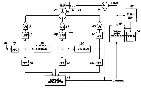
The circuitry illustrated in Fi~ure 1 i6 a
chroma~luma separator which separates the chrominance and
luminance components of composite video signal In addition
circuitry is included for enhancing the vertical detail of
the luminance component. In Figure 1 baseband analog
composite video signal is applied from, for example, -tunex
circuitry (not shown) to input terminal 10. This signal is
coupled to the analog-to-digital converter (ADC) 12 wherein
it is converted to plural-bit binary samples and at a rate
sufficient to satisfy the Nyquist sampllng criterion.
13~3212
-3- RCA 84945/84945A
Samples from the ADC 12 are coupled to the low
pass filter 14, the high pass filter 38 and the delay
element 18. Low pass filter 14 attenuates signal
frequencies occurring in the frequency spectrum normally
occupied by the chrominance component of composite video
signal. High pass filter 38 attenuates signal frequences
occurring below the spectrum normally occupied by the
chrominance component. Filter 38 (and filters 40 and 44)
may be chrominance band pass filters. Alternatively the
filter function of filter 38 may be realized by subtracting
the output of low pass filter 14 from the signal coupled to
its input. In this instance filters 14 and 38 will have
complementary frequency response characteristics. Delay
element 18 delays samples by one horizontal line period and
has its output coupled to low pass filter 20, high pass
filter 40 and delay element 30. Delay element 30 delays
samples by one horizontal line period and has its ou-tput
coupled to low pass filter 32 and high pass filter 44.
High pass filters 40 and 44 are similar to high pa~s filter
38 and low pass filters 20 and 32 are similar to low pass
filter 14. High pass iltered samples from filters 38, 40
and 44 are coupled to the chrominance separator 42 which
produces the chrominance component of composite video
signal. Chrominance separator 42 may be of the.type
disclosed in U.S. Patent No. 4,636,840 issued 1/13/87-i~o
McNeely and Fling or of the type disclosed in U.S. Patent
NO. 4,050,084 issued September 20, 1977 to Rossi.
Low pass filtered composite video signal from
filters 14, 20 and 32 are respectively scaled by factors
1/4, l/2, and l/4 by scaling circuits 16, 22, and 34.
Scaled samples from weighting circuit 22 are summed with
the negative of scaled samples from scaling circuits 16 and
34 in the combining circuit 24. The combined signal
provided by circuit 24 is related to vertical or
line-to-line changes of the low frequency luminance
component. The signal provided by combining circuit 24 is
coupled to a non-linear-processor (NLP) 26. NhP 26 may be
one of several different functional elements. For example
~l3C~32~2
-4- RCA 84945/84945A
NLP 26 may include a differentiator to generate peaking
signals occurring only at vertical transitions having
predetermined minimum amplitudes. Alternatively NLP 26 may
be a non-linear gain element which cores signal in a first
amplitude range, amplifies signal in a second intermediate
amplitude range and attenuates signal in a third large
amplitude range. Apparatus of this latter type is
described in U.S. Patent No. 4,422,094.
Signal from NLP 26 and delayed composite video signal
from delay element 18 are combined in signal combining
circuit (SCC) 28 to produce composite video with lower
frequency components (related to vertical transitions)
enhanced. Signal from SCC 28 and signal from chrominance
separator 42 are coupled to subtracter 36 wherein the
chrominance component is subtracted from the composite
video signal to produce the luminance component.
Luminance signal from subtracter 36 is coupled to
processor 39 and sync separator 37. Sync separator 37
extracts the synchronizing components from the luminance
signal and develops the necessary signals to appropriately
control both the processor 39 and the display element 38.
Chrominance signal from separator 42 is coupled
to processor 39 which appropriately conditions and combines
the chrominance and luminance components to produce signa~s
for driving the display device 38. ~
Refer next to Figure 2 which illustrates three
sets of signals, which signals are drawn especially to
emphasize the problem overcome by the invention. In the
left portion of the drawing are four waveforms intended to
represent four successive horizontal~lines of low frequency
composite video signal which may be available from low pass
filters 14, 20 and 32. The timing interval T1 corresponds
to the occurrence of the horizontal synchronizing signal in
each line interval. The video signal is intended ~o be
identical from line-to-line except at interval T2. Between
the occurrence of lines n+l and n~2 a sig~al change occurs
during the interval T2 within the horizontal period. This
13~3Z~Z
, .
-5- RCA 84945/84945A
change represents a ver-tical transition in the image to be
displayed.
At any instant samples representing three
vertically aligned picture elements (pixels) from three
successive lines are output by low pass filter 14, 20 and
32. For example if ADC 23 is currently converting line
n+3, then filters 14, 20 and 32 are currently producing
filtered samples from lines n+3, n+2 and n+1 respectively.
Due to the selection of scale factors for elements 16, 22
and 34, the combined signal provided by combining element
24 is weighted to correspond to vertical transitions
attendant the horizontal line provided by delay element 18.
Si~nals provided by combining element 24 are
combined with signals from delay element 18 in SCC 28. The
set of signals drawn in the center of the Figure 2
represent the output signals from combining element 24.
The signals produced by element 24 are drawn adjacent the
low freguency components of the composite video lines
corresponding to the wideband composite video line with
which it is combined in SCC 28. The signals from element
24 are zero valued except where a line-to-line difference
occurs. A single transit,ion between line intervals may be
reflected in two line intexvals as shown in Figure 2. Note,
howevér, that uniform changes over three or more lines will
not produce (from the output of element 24) signals
indicating the occurrence of such changes.
The set of signals drawn to the right of the
Figure 2 repxesent the sum of the horizontally adjacent
signals to the left and center of ~he figure. It can be
seen in the set of signals to the right of the Figure 2,
that during the interval T2 for line n+2, the amplitude of
the combined signal is equal to the amplitude of the
synchronizing components at interval T1. It will be
readily appreciated that if the sync separator 37 is to
detect the horizontal synchronizing signal as a function of
its amplitude, it will pçrforce erronously detect interval
T2.
~L3~3Z12
-6- RCA 84945/84945A
In order to preclude this happenstance, but
otherwise not affect circuit performance, the signal
combining circuit SCC 28 is designed to preclude the
additive signal from NLP 26 from extending the luminance
signal into the amplitude range of the synchronizing
component.
Figure 3 illustrates a first embodiment of a
signal combining circuit which may be implemented for SCC
28. In Figure 3 video signal from, for example, delay
element 18 is applied to bus 50, and enhancing signal from,
for example NLP 27 is applied to bus 58. Bus 50 is coupled
to one input of adder 57 and to the subtrahend input of the
subtracter 52. A reerence value from source 53 is applied
to the minuend input of the subtracter 52. The reference
value, in this example, corresponds to black level or the
most negative amplitud~ that the luminance signal is
expected to attain in the active portion of a line
interval. Subtracter 52 produces a signal corresponding to
an inverted version of the signal applied on bus 50 and
which is offset by the reference value. For the reference
value being positive and equal to black level, the output
signal from subtracter 52 will be negative valued for input
signal amplitudes that are more positive than black level,
zero valued for input signal amplitudes equal to black
level, and positive valued for input signal amplitudea less
positive than black level.
Subtracter 52 produces value bits and a sign bit
which is presumed to be a logic one for negative output
values and a logic zero for positive output values. The
value bits provided by subtracter 52 are coupled to
mutually exclusive first input terminals of a bank of
two-input AND gates 5~. The si~n bit is coupled to the
second input of each of the ~N~ gates in bank 54. The AND
gates 54 are conditioned by the sign bit to pass negative
differences produced by subtractex 52 but provide zero
values for positive differences. The values provided by AND
gates 54 include the sign bit which may be routed through
an AND gate in the bank of gates 54 or it may be routed
~3~P3Z~L~
-7- RCA 84945/84945A
around the AND gates. In either case it is desired that
the signal provided by AND gates 54 be in two's complement
format.
The output values from AND gates 54 are coupled
to the minuend input port of a second subtracter 55 and to
one input port of a multiplexer 56. The enhancing signal
on bus 58 is coupled to the subtrahend input port of
subtracter 55 and to a second input port of multiplexer 56.
The polarity indicating sign bit from subtracter 55 is
coupled to the control input terminal of multiplexer 56.
The output of multiplexer 56 is coupled to a second input
of adder 57.
Subtracter 55 will produce negative values
whenever the signal from the AND gates 54 are more negative
than the enhancing signal on bus 58. When this condition
is satisfied, the enhancing signal, when added to the
signal on bus 50, in adder 57, cannot pull the amplitude of
the combined signal below the black level. If the output
of subtracter 55 i.s positive, this indicates that the
combination of the enhancing signal on bus 58 and the video
signal on bus 50 will undesirably combine to produce
amplitudes more negative than black level. Therefore when
the subtracter 55 produces negative differences multiplexer
56 is conditioned to couple the enhancing signal on bus 5
to the adder 57. The output of adder 57 is the video~
signal enhanced in accordance with the signal on bus 58.
Alternatively, when subtracter 55 produces
positive differences, multiplexer 56 couples the signal
from the AND gates 54 to adder 57. This will only occur
for negative valued signals on bus 58 because of the
polarity discrimination performed by the AND gates. When
the si~nal from the AND gates 54 is negative and combined
with the video signal in adder 57, the amplitude of the
combined signal is pulled to black level, since the signal
from the AND gates 54 is a DC offset, negative version of
the video signal.
The signal from the AND gates 54 is shown coupled
directly to the multiplexer 56. In an alternative
13V32~LZ
-8- RCA 84945/84945A
embodiment the signal ~rom the AND gates may be scaled by,
e.gO bit shifting, or it may be processed in some other
manner.
Consider the input video signal from bus 50 to
include a composite si~nal including a chrominance
component in the form o~ a modulated subcarrier, the
chrominance component occupying less than the entirety of
the frequency passband of the composite signal. For
certain amplitude signals, the difference provided by th~
bank of AND gates 54 may be greater and less than the
enhancing signal for alternate half cycles of the
subcarrier. In this instance the sign bit signal
controlling the multiplexer 56 will oscillate between one
and zero values and create an undesirable artifact in the
output signal. In order to preclude this circumstance a
filter S1 may be inserted between the bus 50 and the
s~trahend input port of subtracter 52. The filter 51 may
be a low pass filter designed to attenuate signals in the
fre~uency band normally occupied by the chrominance
component, or it may be a chrominance trap.
Figure 4 illustrates a second embodiment of the
combining circuit SCC 28. Elements in Figure 4 designated
with like numerals as elem~nts in Figure 3 are identical
and perform like functions.
In some systems the black level may not be
defined and thus a fixed black level reference for
application to the minuend input port of subtracter 52 may
not be easily selected. To overcome this difficulty the
Figure 4 SCC includes apparatus 100 for adaptively
d~termining the reference value.
A ~irst embodiment of circuitry 100 includes a
D-t~pe latch 72, having a data input port coupled to the
input bus 50 and a data output, Q, coupled to the minuend
input port of the subtracter 52 ~via the dashed
connection). The clock input terminal, C, of latch 72 is
coupled to a source of pulses, ~ , which provides, e.g.,
one pulse per line interval, during the time interval that
black level occurs in the video signal. Black level is
~3~32~2
-9- RCA 84945/84945A
loaded into latch 72 by the action of pulse Hp and applied
to subtracter 52 for the duration of each line interval.
Alternatively, if it is anticipated that the signal will
contain noise, it will be advantageous to average the black
level values that are sampled during successive line
intervals and apply the averaged value as the black level
reference value.
Nominally black level occurs in the video signal
immediately following the horizontal synchronizing pulses~
The signal pulse ~ may therefore be derived from the
detected pulses.
A second embodiment which includes elements
72-82, develops the difference between black level and the
tip of the synchronizing component as the reference value.
The video signal on bus 50 is coupled to the data input
port of latch 72 and to the subtrahend input port of
subtracter 74. The output of latch 72 is coupled to the
minuend input of subtracter 74. The pulses Hp coupled to
the clock input terminal of latch 72 are timed to load the
value of the synchronizing component into the latch. For
the duration of the synchronizing component, subtracter 74
will produce a zero valued output sinc~ the same input
value will be coupled to both of its input ports. At the
trailing transition of the synchronizing pulse when the
signal amplitude moves to black level, subtracter 74 ~-
~develops a negative valued output. At this time the sign
bit of the difference provided by suhtracter 74 changes
from a zero to a one state. The sign bit is coupled to the
set input terminal of a set-reset flip flop 76 which is
reset by the pulses ~ . The output of flip flop 76 is
coupled to the clock input of latch 80 via a delay element
78. The difference ou~put from subtracter 74 is coupled to
the data input port of latch 80. When the output of flip
flop 76 changes state responsive to the sign bit from
subtracter 74, this transition is delayed several sample
periods in delay element 78 (to insure that the trailing
transition of the synchronizing pulse has reached its
maximum value) and coupled to latch 80 to store the current
~3(J;~2~
-10- RCA 84945/84945A
diference value from subtracter 74. This value represents
the difference between the black level and the tip of the
horizontal synchronizing pulse. No further values are
stored in latch 80 until after the next occurrence of pulse
Hp. Successive values output from latch 80 are averaged in
the element 82. These values are negative valued due to
the arrangement of input connections to the subtracter 74.
The averaged values are therefore complemented and then
coupled as the reference valué to subtracter 52.
The averager 82 may be eliminated if desired. In
addition it may be desirable to filter or core the video
signal applied to apparatus 100 in order to preclude noise
from interfering with the detection of the reference value.
In Figure 4, a multiplexer 88 and reference
source 86 have been substituted for the bank of AND gates
54 in Figure 3
The output of subtracter 52 is coupled to one
input port o multiplexer 88 and the source 86 is coupled
to a second input port of multiplexer 88. The sign bit
output from the subtracter 52 is coupled to the control
input of multiplexer 88 and conditions the multiplexer to
couple source 86 or subtracter 52 to its output for the
subtracter 52 providing positive and negative differences
respectively.
If the source 86 provides zero valued referonce
values then multiplexer 88 and source 86 emulate the AND
gates 54 exactly. Alternatively if the source 86 is
selected to provide negative reference values, negative
peakin~ egual to the reference magnitude from source 86 can
be applied to blacker than black signals. If the reference
values are positive, blacker than black signal values will
be offset positively by a value at least equal to the
positive reference value.
Further modifications of the peaking function may
be realized by adding a DC offset to the averaged value
provided by averager 82 to subtracter 52.
The embodiments of Figures 3 and 4 are directed
to limiting peaking in the negative sense; however they can
.
~L3~3Z~2
, .
~ RCA 84945/84945A
readily be adapted to limiting in the positive sense as
well. For example to preclude peaking greater than a
predetermined white level, a predetermined white level will
be applied as the reference to subtracter 52, the sign bit
from subtracter 52 will be complemented before being
coupled to the control inputs of the bank of gates 54, and
the two signals supplies to subtracter 55 will be
interchanged.