Note : Les descriptions sont présentées dans la langue officielle dans laquelle elles ont été soumises.
1~04768
MULTIPLE CONTROL CIRCUIT
1 The present invention relates to a multiple control
circuit for use with an electronic control device for an
automobile, and more specifically to an anti-lock brake control
assembly used to control automobile brakes.
Modern automobiles are equipped with various types of
electronic control devices to control their running
conditions. Among them, an anti-lock brake control device
used to control an automotive brake is expected to work in
an extremely reliable manner in view of the fact that the
failure of the braking device directly leads to endangerment
of the passenger's lives.
Various types of anti-lock brake control devices are
now available. They basically operate as follows: A
plurality of sensors provided at the front and rear wheels
detect rotational speeds of the wheels. The signals from
the sensors are converted into pulse signals. A central
processing unit (CPU) computes wheel speeds, reference wheel
speeds (estimated vehicle speed) and accelerations on basis
of the input signals. If a driver abruptly applies the brake
when the car is running on a slippery road surface, the
wheels tend to lock. In an ordinary anti-lock system, the
CPU detects such an abnormal state of the wheels by
comparing the wheel speeds with the reference wheel speeds
,1~
~04768
and provides signalsto brake pressure control valves so as to
release the ~rakes only momentarily and to then apply the brakes again when
the wheels recover to predetermined rotational speeds. In
other words, the valves are controlled so that the
coefficient of friction between the wheels and the road
surface will be maintained at its maximum.
Such anti-lock brake control involves releasing brakes
even while the driver is applying brakes. If any of the
anti-lock control systems should become out of order or
malfunction, a serious accident will result. Thus, it has
been proposed to provide the anti-lock control system with a
means for detecting the malfunction and disabling the anti-
lock control system to return the automobile to its ordinary
braking system.
One example of such anti-lock brake control systems is
disclosed in ~.S. Patent No. 4,546,437, which will be
described with reference to Fig. 3.
In this system, signals from four sensors which
represent the respective wheel speeds are processed at a
pulse processing unit and fed in parallel to two independent
microcomputers(0)and (l)which operate synchronously with
each other. The information stored in the microcomputers I
and II is exchanged therebetween. One of the microcomputers
is adapted to control a valve actuating circuit to open and
close brake pressure control valves. At the same time, the
, . . . i,
1~04768
output signals from the valve actuating circuit are fed to
the other microcomputer for monitoring after having been
level-converted. The outputs of the latter microcomputer
are in turn fed to the former microcomputer. Thus, both
microcomputers monitor and supervise the output signals of
their counterparts.
Another brake control device shown in Fig. 4 is also
known in which the sensor signals for all the wheels are fed
to a microc~ter (0) to -ontrol brake pressure control
valves for the front wheels. The same sensor signals for
all the wheels are fed to another microcomputer S'l) to
control brake pressure control valves for the rear wheels.
These two independent microcomputers mutually monitor the
output signals of their counterparts to detect any
abnormality of the signals.
In another conventional type of brake control device,
three microcomputers are provided to control a respective
brake pressure control valves, one pair assigned to the
front right wheel, another pair to front left wheel and a
third pair to both rear wheels. Their output signals are
under mutual surveillance.
With the first-mentioned anti-lock brake control
device, disclosed in U.S. Patent No. 4,546,437, if multiple
malfunctions should take place simultaneously in the control
circuit e.g. if the microcomputer for controlling the
~,
1;~04768
solenoid valves for brake pressure control should go wrong
and the other microcomputer for monitoring the former one
shou~d fail to detect its abnormality, abnormal valve
control signals might be sent. In view of this and other
conceivable failure modes, this device is not necessarily
satisfactory in preventing the failures and malfunctions of
the circuit.
With the second prior art control device, there is a
possibility that at least two lines at one side may suffer
the same problem as described above with the first~mentioned
prior art.
With the third prior art control device, since the
three lines are controlled independently, the failure rate
inevitably increases and the production cost is high.
In any of the abovesaid prior art devices, the output
signals of the microcomputers are directly fed to the valve
actuating circuits. The output signals of one microcomputer
are kept under surveillance by the other microcomputer, or
two microcomputers operate independently of each other.
None of the prior art brake control devices are adapted to
cope with multiple malfunctions in such a way as to control
the vehicle toward the safer side according to the output
signals.
It is an object of the present invention to provide a
multiple control circuit which obviates the abovesaid
768
1 shortcomings.
In accordance with the present invention, there is
provided a multiple control circuit comprising: at least
two input processing circuits provided independently of each
other for processing a plurality of input signals; at least
two control logic circuits provided in parallel to each
other so as to operate independently and synchronously for
receiving the output signals from the respective input
processing circuits to perform logic operations according to
a predetermined program to give control signals; an output
decision logic circuit for receiving the signals from the
control logic circuits to perform logic operat.ions according
to AND logic, OR logic, or combination of AND and OR logics
to decide the outputs; at least two comparator circuits for
comparing the outputs of the output decision circuit with
the outputs of the control logic circuits to give a
discrepancy signal if they differ from each other; and a
failsafe output circuit for giving a failsafe output signal
upon receipt of the discrepancy signal from one of the
comparator circuits, whereby disabling a system is
controlled.
Input signals from sensors are converted into digital
signals by an A/D converter circuit. The digital signals are
fed in parallel to two or more input processing circuits for
input processing and then sent to the respective control
~04768
1 logic circuits. Upon receiving the input signals, each
control logic circuit executes logic operations in
accordance with a program stored therein to output control
signals for controlling the valve actuating circuits.
The control signals from the two or more control logic
circuits should be identical to one another if they operate
normally. But practically, the control signals which flash
momentarily cannot always be identical to one another due to
malfunction or failure of either of the control logic
circuits, noise or time lag. If such signals are fed
unchecked, the actuating circuits might malfunction.
According to the present invention, the output signals of
the control logic circuits are fed to the output decision
loqic circuits where logic operations are carried out by an
AND logic element, an OR logic element or the combination of
AND and OR logic elements. If the signals of all the
control logic circuits are the same as one another, the
output decision circuits output the signals as they are. If
not, their output signals coincide with the output signals
of some of the control circuits. The output signals of the
other control circuits does not coincide with the outputs of
the output decision circuits. If this discrepancy signal
persists for a predetermined period of time, a failsafe
signal occurs, disabling the controlled system. More
specifically, if the output signals of any of the control
1:~0~68
1 circuits should differ from the other outputs, the
comparator circuits will pick up this difference, causing
the failsafe output circuit to send out a failsafe signal.
With this failsafe signal, the actuating mechanism for the
controlled system is partially or completely turned off,
thus disabling the entire system being controlled. Thus,
the controlled system is assured of its utmost safety and
optimum operation by multiple control circuits of the
present invention.
In another of its aspects this invention provides
for a control apparatus for controlling a plurality of slip
control devices of an automobile, said control apparatus
comprising a plurality of non-redundant sensor means for
outputting sensor signals; redundant control logic circuits
for receiving the sensor signals from each of said sensor
means as redundant signals, processing said redundant
signals, and outputting a plurality of sets of redundant
control signals for controlling the plurality of slip
control devices; an output decision logic circuit having a
plurality of logic means selected from a group comprising
AND logic means, OR logic means and a combination of AND and
OR logic means, each of said logic means having as inputs a
different set of the plurality of redundant control signals,
and each for outputting a non-redundant control signal for
independently controlling one of the plurality of slip
control devices; a plurality of comparator means for
..
.
1304768
1 comparing said non-redundant control signals outputted by
each of said plurality of logic means with signals outputted
by each of said plurality of control logic circuits and for
outputting a discrepancy signal if the thus compared signals
are different from each other and if this state continues in
excess of a predetermined period of time; a disablement
means for dissabling at least one of said slip control
devices in response to said discrepancy signal being
outputted by at least one of said plurality of comparator
means.
Other features and objects of the present
invention will become apparent from the following
description taken with reference to the accompanying
drawings, in which:
Fig. 1 is a block diagram of the multiple control
circuit embodying the present invention adapted for use with
an anti-lock brake control assembly;
Fig. 2 is a block diagram of the output decision
logic circuits of the same; and
Figs. 3 and 4 are block diagrams of conventional
anti-lock brake control circuits.
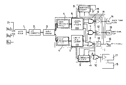
Now, referring to the drawings, Fig. 1 shows an
embodiment of the multiple control circuit according to the
present invention applied to an anti-lock brake control
circuit for a motor vehicle. The elements of the multiple
control circuit are delineated by heavy lines, and the other
parts of the anti-lock brake control circuit such as an
7a
~.
, ~, "S,:_f
1~04768
1 input unit, A/D converter and valve actuating circuits are
indicated by fine lines. Sensors Sl to S4 are provided to
detect the rotational speeds of wheels and output the
information on the wheel speeds as analog signals. The
analog signals are sent through an input stage 1 to a
digitizer such as an A/D converter 2 where they are
converted into pulse signals. The pulse signals are stored
temporarily in an input buffer 3 and fed in a parallel
relation with one another to a plurality of (two in the
preferred embodiment) control systems of the multi-line
control circuit.
The multiple control circuit comprises two independent
input processing circuits 4, 4' for computinq and processing
the pulse number and spacings of the pulse signals and two
control logic circuits 5 and 5' for carrying out logic
operations on the output signals from the respective input
processing circuits according to a predetermined program to
output control signals. The control logic circuits 5 and 5'
are provided in parallel and operated independently, but
synchronously, with each other.
The control signals from the control logic circuits 5
and 5' function to close and open solenoid valves for
controlling the brake pressure in an anti~lock brake
assembly which will be described later. The logic circuits
5 and 5' may be microcontrollers or one-chip microcomputers
~,.
~s04768
1 adapted to be operated according to the same one program.
Its logic operation comprises e.g. the steps of
calculating from the input signals the ever-changing wheel
speeds, determining a reference wheel speed by use of a
formula for estimating vehicle speeds from the wheel speeds,
and outputting control signals for shifting the mode of the
solenoid valve from pressure increase to pressure reduction
or pressure holding if the wheel speed becomes lower than
the reference wheel speed.
Whether pressure should be reduced or held depends upon
the difference between the wheel speed and the reference
wheel speed. Lower wheel speed than the reference wheel
speed indicates that the slip ratio of the wheels is too
high and that the frictional forces by the tires are not
effectively utilized to brake the automobile. In that case,
braking forces are reduced momentarily. As the slip ratio
begins to reduce, the pressure control mode is returned to a
pressure increase or pressure holding position. The wheels
are thus prevented from locking.
The multi-line control circuit has an output decision
logic circuit comprising two AND logic circuits 6 and 7 and
an OR logic circuit 8. These circuits give control signals
to three solenoid valves 14, 15 and 16 through three valve
control circuits 11, 12 and 13 to close and open the
solenoid valves. The solenoid valves 14, 15 and 16 are used
~04~68
1 for the front right wheel, front left wheel and both rear
wheels, respectively.
Fig. 2 shows the details of the output decision logic
circuit which is enclosed in dashed line. Other related
parts are shown by fine lines. Each solenoid valve
comprises an intake valve and an exhaust valve. Thus
six valves are used for the front right wheel, front left
wheel and both rear wheels. In Fig. 2, reference characters
I and E are attached to numerals to distinguish the intake
valve lines from the exhaust valve lines. The output
decision logic circuits for the front right wheel and for
the front left wheel function as AND logic circuits which
satisfy the following formulas:
I = Io Il
E = Io . Eo . Il . El = I (Eo . El)
(wherein I and E are outputs from the lines, and Iol Il, E
El are outputs from the control logic circuits 5 and 5' in
which Io and Eo are from circuit 5 and Il and El are from
circuit 5')
The output decision circuit for the rear wheels
functions as an OR logic circuit which satisfies the
following formulas:
I = Io Il + Io El + Il Eo
E = (Il El + Io-Eo)
If one or both of the control logic circuits (one-chip
~ .
`` 1;~0~768
1 microcomputers) should get out of control, watch dog signals
WD are inputted to NOR elements 6 E~ 6 I' 7 E~ 7 I' 8 E~ 8 I
to forcibly turn off all the outputs of the output decision
circuits. In other words, no outputs are sent out as long
as the WD signals are high level signals (hereinafter
referred to as H). Normally, the watch dog signals are low
level signals (hereinafter referred to as L). Thus, if the
other input of each line is L, the output is H and if the
input is H, the output is L. Since the logic elements
located upstream of the NOR elements 6~E~ 6lI~ 7'E' 7'I are
NAND elements 6E~ 6I~ 7E~ 7I' the output decision logic
circuits for the front wheels constitute AND logic circuits
as a whole, and the one for the rear wheels constitute an OR
circuit since the logic elements located upsteam of the NOR
elements 8IE and 8lI are NOR elements 8E~ 8I.
With reference to the intake valve line for the front
right wheel, for example, if both input signals are H, the
output of the NAND element 6I is L. Normally the other
input signal of the NOR element 6lI is L. Thus, its output
is H. If both input signals are L, the output of the NAND
element 6I is ~ and the output of the NOR element 6lI is L.
Thus, this circuit is an AND logic circuit as a whole. The
same is true of the intake valve line for the front left
wheel (7I~ 7 I~ 12I)-
The exhaust valve lines for both front wheels (6E~ 6
~04768
1 llE and 7E~ 7'E~ 12E) are basically of the same structures
as the intake valve lines except that the outputs I of the
intake valve lines are inputted to the NAND elements 6E~ 7E
as input signals.
The intake valve line for the rear wheels (8I~ 8
13I) constitutes an OR logic circuit comprising NAND
ments 811' 812' 813, 814, an inverter 815 and a NOR
element 8lI. Its exhaust valve line (8E~ 8IE~ 13E) also
constitutes an OR circuit comprising inverters 8El, 8E2 and
NAND elements 8E3~ 8~4.
The multiple control circuit including the output
decision logic circuits further comprises comparator
circuits 9 and 9' and a failsafe output circuit 10 as shown
in Fig. 1. The outputs of the output decision logic
circuits are supplied to the actuating circuits 11, 12 and
13 for the solenoid valves 14, 15 and 16 and amplified by
the actuating circuits to obtain the valve actuating
signals. The comparator circuits compare the valve actuating
signals with the output signals of the control logic
circuits 5 and 5'.
The failsafe output circuit 10 sends out a failsafe
output signal upon receiving from either of the comparator
circuits a signal indicating the discrepancy between the
signals compared. The failsafe output signal is given to an
actuating circuit 17 of a failsafe relay 18 for turning on
~. .
1~04768
1 and off the power to the solenoid valves 14, 15 and 16 to
switch off the failsafe relay and partially or completely
disabled the anti-lock brake control unit. As shown at
lower part of Fig. 2, the failsafe output circuit 10
comprises NOR elements 10' and 10'' and an inverter 10'''
interposed therebetween. The watch dog signal fed to the
output decision logic circuits is given to the circuit 10 as
well.
The failsafe output circuit 10 is a negative logic
circuit. Thus, if either of the output signals of the
comparator circuits 9, 9' is a discrepancy signal (H), the
output signal of the NOR element 10' will be L, the output
signal of the inverter 10''' will be H, and hence one of the
input signals of the NOR element 10'' will be H. Since the
WD signal is normally L, the output signal of the NOR
element 10'' will be L. This low level signal turns off the
actuating circuit 17, thus turning off the failsafe relay
18. Te anti-lock brake control assembly is thus partially
or completely disabled. This means that the output signals
of the comparator circuits 9 and 9' function as failsafe
signals. In order to allow the actuator for the anti-lock
brake control assembly to operate normally, the failsafe
relay has to be turned on. This condition is established
only if both the WD signal and the output signal of the
inverter 10''' are L. Thus the output signals of the
,~ ~
J
l~o~a
1 comparator circuits 9 and 9' have to be L as well.
The logic structure of the output decision circuits
will now be described. A pair of intake and exhaust
solenoid valves are used in the respective lines for the
front right wheel, front left wheel and both rear wheels.
Brake pressures are controlled in one among three positions
i.e. pressure increase, pressure holding and pressure
reduction by changing the combination of control input
signals for these valves.
TABLE 1
Intake Exhaust Brake
valve (I) valve (E) pressure
__
OFF (L) OFF (L) Pressure increase
(normal state)
ON (H) OFF (L) Pressure holding
ON (H) ON (H) Pressure reduction
OFF (L) ON (H) (Inhibition output)
(non-use)
The outputs of the control circuits 5, 5' (CPUO and
CPUl) are simultaneously fed to the output decision logic
circuits. Table 2 shows the relationship between the output
signals of both the CPUs and those of the output decision
logic circuits which are the results of logic operations of
the outputs of the CPUs.
14
.~
.. ..
~0~8
TABLE 2
For right front and left front wheels . . . AND logic
. ._
\ CPVO Pressure Pressure Pressure Inhibition
CPU ~ increase holding reduction output
_ I \ (I,E)=(L,L) (I,E)=(H,L) (I,E)=(H,H) (I,E)=(L~H)
Pressure Increase Increase Increase Increase
increase
(I,E)=(L,L) (L,L) (L,L) (L,L) (L,L)
Pressure Increase Holding Holding Increase
holding
(I,E)=(H,L) (L,L) (H,L) (H,L) (L,L)
Pressure Increase Holding Reduction Increase
reduction
(I,E)=(H~H) (L,L) (H,L) (H,H) (L,L)
Inhibition Increase Increase Increase Increase
output
(I,E)=(L,H) (L,L) (L,L) (L,L) (L,L)
For both rear wheels . . . OR logic
\ CPUO Pressure Pressure Pressure Inhibition
CPUI ~ increase holding reduction output
\ (I,E)=(L,L) (I,E)=(H,L) (IJE)=(H,H) (I,E)=(L,H)
Pressure Increase Holding Reduction Increase
increase
(I,E)=(L,L) (L,L) (H,L) (H,H) - - (L,L)
Pressure Holding Holding Reduction Increase
holding
(I,E)=(H,L) (H,L) (H,L) (H,H)_ _(L,L)
Pressure Reduction Reduction Reduction Increase
reduction
(I,E)=(H,H) (H,H) (H,H) (H,H) (L,L)
.
Inhibition Increase Increase Increase Increase
output
(I,E)=(L,H) (L,L) (L,L) (L,L) (L,L)
~s04768
In Table 2, if the output signals of the CPU0 and CPUl
are different from each other e.g. if the output signals of
the CPV0 are for pressure holding and those of the CP~l are
for pressure reduction, the output decision logic circuits
will output pressure holding signals which are different
from the output signals of the CPUl. In such a case, the
comparator circuit 9' produces a discrepancy signal (H) and
thus the failsafe output circuit 10 produces a failsafe
output signal. However, if the duration of the presence of
different output signals of the CPUs is too short, the
failsafe signal will not be produced. Whether or not to
produce a failsafe signal is decided by the CPUs according
to the duration of different signals.
In the preferred embodiment, a duration of 8
lS milliseconds (ms) is the borderline. If different signals
should last longer than 8 ms, the failsafe signal will be
produced while maintaining the operation as shown in Table
2. If the discrepancy of signals is corrected within 8 ms,
the failsafe output signal will not be produced and brake
control will be executed according to Table 2. If the
failsafe signal is produced, the failsafe relay 18 will be
turned off to partially or completely cut off the electrical
circuit from the hydraulic actuators of the anti-lock brake
control assembly, thus disabling the entire control
assembly.
16
.,
.~ . ,~,
`` 130~768
1 From Table 2, it will be understood that if the outputs
of the CPUO a~d CPUl are different from each other, the
output decision logic circuit selects and outputs the
signals on the pressure increase side for the front wheels
according to AND logic, and the signals on the pressure
reduction side for the rear wheels according to OR logic.
With this arrangment, if the output signals of the two CPUs,
which must be indentical, should be different from each
other because of the malfuction of one or both of the CPUs,
noises or time lags between the output signals from the
CPUs, the front wheels are controlled by the signals on the
pressure increase side so as to be braked with a greater
brake pressure. On the other hand, the rear wheels are
controlled by the signals on the pressure reduction side so
as to be braked with a smaller brake pressure to maintain
the stability of the vehicle.
The front wheels and the rear wheels are controlled in
opposite ways to each other if the two CPUs should produce
different outputs. This is because the braking force on the
front wheels accounts for 70-80 per cent of the entire
braking force (on both front and rear wheels) owing to the
load distribution factor of the vehicle during braking. It
is known from experience that the front wheels should be
controlled toward the pressure increase side to insure
braking force and the rear wheels should be controlled
1~04768
l toward the pressure reduction side for greater drivability
and stability of the vehicle and to prevent tail swinging.
In the preferred embodiment, we employed a three-
position pressure control including pressure increase;
pressure holding and pressure reduction. It will be readily
understood that two-position control including pressure
increase and pressure reduction is also applicable.
With the prior art anti-lock brake control device,
input signals from sensors are fed in parallel to two
independent central processing units. The outputs of one of
the CPUs are compared with those of the other. If the
outputs of two CPUs are different from each other, it is
judged that there is a malfunction, noise or time lag in one
of the CPUs. Consequently, the anti-lock brake control
assembly is disabled by stopping the transmission of the
control signals. Otherwise, such abnormal control signals
are given unchecked. In contrast, the multiple control
circuit of the present invention is designed to control the
system to be controlled always to the safe side accordinq to
the characteristics of its operation. This is accomplished
by the provision of an output decision circuit which
collects the outputs from at least two control logic
circuits and decides which to output.
It will be needless to say that the multiple control
circuit of the present invention is applicable to other
18
~04~768
electronic control devices s~ch as a traction controller,
rather than the anti-lock control assembly.
1 9
... .