Note : Les descriptions sont présentées dans la langue officielle dans laquelle elles ont été soumises.
13~ 9
--1--
CRYSTALLINE RARE EARTH ALKALINE EARTH
COPPER OXIDE THICK FILM CONDUCTOR
Field of the Invention
The present invention relates to thick film
electrical conductors.
Background of the Invention
The term ~superconductivity~ is applied to
the phenomenon of immeasurably low electrical
resistance exhibited by materials. Until recently
superconductivity had been reproducibly demonstrated
only at temperatures near absolute zero. As a
material capable of exhibiting superconductivity is
cooled, a temperature is reached at which resistivity
decreaseæ (conductivity increases) markedly as a
function of further decrease in temperature. This is
referred to as the superconducting transition
temperature or, in the context of superconductivity
investigations, ~imply as the critical temperature
(Tc). Tc provides a conveniently identified and
generally accepted reference point for marking the
onset of superconductivity and providing temperature
rankings of superconductivity in differing materials.
It has been recently recognized that certain
rare earth alkaline earth copper oxides exhibit
superconducting transition temperatures well in excess
of the highest previously known metal oxide Tc, a
13.7K Tc reported for lithium titanium oxide.
These rare earth alkaline earth copper oxides also
exhibit superconducting transition temperatures well
in excess of the highest previously accepted
reproducible Tc, 23.30K for the metal Nb3Ge.
Recent discoveries of higher superconducting
tran8ition temperatures in rare earth alkaline earth
copper oxides are reported in the following
publications:
P-l J.G. Bednorz and K.A. M~ller, 'IPossible High
Tc Superconductivity in the Ba-La-Cu-0 System", Z.
Phys. B. -Condensed Matter, Vol. 64, pp. 189-193
,, ~.
,'~J~,
,~,., .~, . . .... .. .
~` 13~S~ 9
. -2-
(1986) revealed that polycrystalline compositions of
the formula BaXLas-XCU505(3-Y)
and 0.75 and y>O exhibited superconducting
transition temperatures in the 30K range.
P-2 C.W. Chu, P.H. Hor, R.L. Meng, L. Gao, Z.J.
Huang, and Y.Q. Wang, ~Evidence for Superconductivity
above 40 K in the La-Ba-Cu-O Compound System",
Physical Review Letters, Vol. 53, No. 4, pp. 405-407,
Jan. 1987, reported increasing Tc to 40.2K at a
pressure of 13 kbar. At the end of this article it is
stated that M.K. Wu increased Tc to 42K at ambient
pressure by replacing Ba with Sr.
P-3 C.W. Chu, P.H. Hor, R.L. Meng, L. Gao, and
Z.J. Huang, "Superconductivity at 52.5 K in the
Lanthanum-Barium-Copper-Oxide System", Science
Reports, Vol. 235, pp. 567-569, Jan. 1987, a Tc f
52.5K for (LaO gBaO.1)2CuO4_y g
pressures.
P-4 R.J. Cava, R.B. vanDover, B. Batlog, and E.A.
Rietman, ~Bulk Superconductivity at 36 K in
Lal 8SrO 2CuO4", hysical Reviçw ~etters, Vol
58, No. 4, pp. 408-410, Jan. 1987, reported
resistivity and magnetic susceptibility measurements
in La2 xSrxCuO4, with a Tc at 36.2K when
x = 0.2.
P-5 J.M. Tarascon, L.H. Greene, W.R. McKinnon,
G.W. Hull, and T.H. Geballe, "Superconductivity at 40
K in the Oxygen-Defect Perovskites La2 xSrxCuO4 yll,
Science Re~Qrts, Vol. 235, pp. 1373-1376, Mar. 13,
1987, reported title compounds (0.05 < x < 1.1)
with a maximum Tc f 39.3K.
P-6 M.K. Wu, J.R. Ashburn, C.J. Torng, P.H. Hor,
R.L. Meng, L. Gao, ~.J. Huang, Y.Q. Wang, and C.W.
Chu, "Supercontuctivity at 93 K in a New Mixed-Phase
Y-Ba-Cu-O Compound System at Ambient Pressure",
physical ~eview Letters, Vol. 58, No. 9, pp. 908-910,
Mar. 2, 1987, reported ~table and reproducible
13t~;2`~`9
-3-
superconducting transition temperatures between 80 and
93K at ambient pressures for materials generically
represented by the formula (Ll XMx)aAbDy,
where L = Y, M = Ba, A = Cu, D = 0, x = 0.4, a = 2,
5 b = l, and y < 4.
The experimental details provided in
publications P-l through P-6 indicate that the rare
earth alkaline earth copper oxides prepared and
investigated were in the form of cylintrical pellets
produced by forming an intermediate oxide by firing,
grinding or otherwise pulverizing the intermediate
oxide, compressing the particulate intermediate oxide
formed into cylindrical pellets, and then sintering to
produce a polycrystalline pellet. While cylindrical
pellets are convenient articles for cooling and
applying resistance measuring electrodes, both the
pellets and their preparation procedure offer
significant disadvantages to producing useful
electrically conductive articles, particularly
articles which exhibit high conductivity below ambient
temperature - e.g., superconducting articles. First,
the step of grinding or pulverizing the intermediate
oxide on a commercial scale prior to sintering is both
time and energy consuming and inherently susceptible
to material tegradation due to physical stress on the
material itself, erosion of grinding machinery metal,
and handling. Second, electrically conductive
articles rarely take the form of pellets.
Electrically conductive articles commonly include
either thin or thick films forming conductive pathways
on substrates, such as insulative ant semiconductive
substrates - e.g., printed and integrated circuits.
Summarv of the Invention
In one aspect thi8 invention i8 directed to a
circuit element comprising an insulative substrate and
means for providing a conductive path between at least
two locations on the substrate including a thick film
.
.
13~-S2~g
-4-
conductor, the thick film conductor being comprised of
a crystalline rare earth alklaine earth copper oxide
layer having a thickness of at least 5 ~m. The
circuit element is characterized in that the substrate
is selected from among strontium titanate, magnesia
~ and alumina and the crystalline rare earth alkaline
earth copper oxide layer exhibits a superconducting
onset transition temperature in excess of 77K and is
comprised of a RlA2C3 phase, where R represents
rare earth, A repreents alkaline earth and C
represents copper.
The term ~thin film~ is employed to indicate
films having thicknesses of less than 5 ~m, such
films most typically having thicknesses of less than l
~m
The term "thick film" is employed in its art
recognized usage to indicate films having thicknesses
in excess of 5 ~m.
The articles produced of this invention
20 exhibit superconducting transition temperatures and,
optimally, true superconductivity, at temperatures in
excess of 77K, the temperature of liquid nitrogen.
The thick film articles of this invention are
believed to be the first high superconducting
25 tran~ition temperature thick film articles. This
invention further provides thick film articles
exhibiting superconductivity at temperatures in excess
of 77K.
The process of preparing the articles of the
30 present invention is particularly well suited to the
fabrication of electrical circuit components. It is
compatible with the formation of patterned electrical
conductors. It is capable of producing thick films of
desirable electrical conduction properties, including
35 superconducting properties, on a variety of
substrates. The process of the invention is further
capable of producing films with limited substrate
~3~S2~;:9
--5--
interaction.
The articles of this invention can be
fabricated by techniques that avoid the disadvantages
of the prior art. No grinding or pulverizing steps
are required. In addition, the electrically
conductive films can be formed on the substrates with
minimal heating of their supporting substrates.
Further, the conductive films are compatible with
solders, bonding pads, and other commonly employed
electrical conduction path connectors.
Brief Description of the Drawing~
These and other advantages of the invention
can be better appreciated by reference to the
following detailed description of preferred
embodiments considered in conjunction with the
drawings, in which
Figure 1 is schematic diagram showing process
steps and articles produced thereby and
Figure 2 is a cross-sectional view of an
electric circuit component.
Description of Preferred Embodiments
The present invention has as its purpose to
make available electrically conductive articles
exhibiting a rare earth alkaline earth copper oxide
contuctive layer coated on a substrate. The term
"rare earth alkaline earth copper oxide" refers to a
composition of matter containing at least one rare
earth element, at least one alkaline earth element,
copper, and oxygen. The term "rare earth" is employed
to designate yttrium and lanthanides - i.e., elements
of the lanthanide series. ~anthanum, samarium,
europium, gadolinium, dysprosium, holmium, erbium, and
ytterbium are particularly preferred lanthanides. The
term "alkaline earth" indicates elements of Group 2 of
the Periodic Table of elements as atopted by the
American Chemical Society. Calcium, strontium and
barium are preferred alkaline earth elements for the
. ~
,;
" ., ~ :,
. ~ ~
: . , ,
13(~5~9
practice of this invention.
In keeping with the established practice in
the ceramics art of shortening lengthy chemical names
of mixed metal oxides by substituting acronyms based
on the first letters of the metals present, the term
"RAC" is hereinafter employed to indicate generically
rare earth alkaline earth copper oxides. When it is
intended to designate specifically a lanthanide or
yttrium as the rare earth component, L or Y,
respectively, is substituted for R; and when it is
intended to designate specifically strontium or barium
as the ~lkaline earth component, S or B, respectively,
is substituted for A.
Except as otherwise noted, all steps in the
preparation of electrically conductive articles
according to this invention are understood to be
practicable in air at atmospheric pressure. It is, of
course, recognized that increasing the proportion of
ambient oxygen present and operation at elevated
pressures, used separately or together, is generally
compatible with the practice of this invention and can
be employed, although not required.
The present invention can be appreciated by
the schematic diagram shown in Figure 1. In Step A a
composition containing particles of metal-ligand
compounds is obtained. Each particle contains rare
earth, alkaline earth, and copper atoms in the same
ratio desired in the final RAC containing conductive
layer. Further, the atoms are intimately intermixed
80 that the composition of each particle is preferably
essentially uniform. Associated with the metal atoms
and completing the compounds are volatilizable
ligands, which can be all alike or cho8en from among
different ligands.
The particles can be of any size convenient
for coating. The particles can exhibit a mean
diameter up to the thickness of the coating to be
; l31~?5Z~g
formed, but more uniform films are realized when the
mean particle diameters are relatively small in
relation to the thickness of the film to be formed.
The particles are preferably less than about 2 ~m in
mean diameter, optimally less than 1 ~m in mean
diameter. The minimum mean diameter of the particles
is limited only by synthetic convenience.
A preferred technique of this invention for
producing metal-ligand compound particles is to
dissolve the rare earth, alkaline earth, and copper
metal ligand compounds in a mutual solvent and then to
spray the solution through an atomizing nozzle into a
gaseous atmosphere. The solvent is chosen to be
evaporative in the gaseous atmosphere. Thus, the
individual particles are dispersed in the gaseous
atmosphere as liquid particles and eventually come to
rest at a collection site as either entirely solid
particles or particles in which the proportion of
solvent has been sufficiently reduced that each of the
metal-ligand compounds present has precipitated to a
~olid form. In the latter instance the particles by
reason of the residual solvent, now no longer acting
as a solvent, but only as a continuous dispersing
phase, form a paste. The paste constitutes a highly
convenlent coating vehicle. When the particles are
collected in a friable form with all or substantially
all of the initially present solvent removed, it is
recognized that a paste can still be formed, if
desired, by adding to the particles a small amount of
a liguid to promote particle cohesion -i.e., to
constitute a paste.
! Only a very small amount of liquid i8
reguired to promote particle cohesion and thereby form
a paste. Typically the liquid constitutes less than
20 percent of the total composition weight and
preferably less 15 percent of tbe total compositon
weight. While optimum paste consistencies can vary
' ''
," .
- - ,
13(~S2~;3
-8-
depending upon the selection of processes for coating
the paste, it is generally contemplated that the paste
viscosity will be in the range of from S X 104 to 3
X 106 centipoise, preferably from 1 X 10⁵ to 2.5 X
106 centipoise.
While atomization and drying can be
undertaken in air at room temperatures, it is
recognized that any gaseous medium which does not
detrimentally react with the metal-ligand compounds
can be employed. Further, the temperature of the
liquid forming the particles or, preferably, the
gaseous medium can be increased to accelerate the
solvent evaporation rate, provided only that such
elevated temperatures in all instance be maintained
below the thermal decomposition temperatures of the
metal-ligand compounds.
The advantage of solitifying the metal-ligand
compounds while they are trapped within discrete
particles is that bulk separations of the rare earth,
alkaline earth, and copper are prevented. The
particle preparation approach of$ers distinct
advantages over simply evaporating bulk solutions to
tryness in that each particle produced by the process
of this invention contains the desired ratio of rare
earth, alkaline earth, and copper elements. This
produces a solid particle coating composition of
micro8cale uniformity.
In Step B of the preparation process, onto a
substrate are coatet the metal-ligand compound
particle~, preferably combined with a carrier liquid
to form a coatable paste or slurry. The resulting
coated article 1 as schematically shown consists of
substrate 3 ant a layer 5 formed by RAC precursors
(metal-ligand compounds) and film forming solvent.
Although the layer 5 is 8hown coextensive with the
substrate 3, it is appreciated that the particles are
well 8uited, particularly when coated in the form of a
~ .
,
13(~S2~9
paste or slurry, to being laid down in any desired
pattern on the substrate. The paste can, for example,
be deposited by any of a variety of conventional image
defining coating techniques, such as screen or gravure
5 printing. Since thick conductive films are most
commonly formed in the art by screen printing, the
present invention is highly compatible with
conventional printed circuit preparation processes.
In Step C article 1 is heated to a
temperature sufficient to volatilize at least a
portion of the ligands and the film forming solvent.
The element 7 resulting consists of substrate 3 and
intermediate layer 9. In its intermediate form the
coating exhibits relatively low levels of electrical
conductivity. The exact form of the intermediate
coating depends upon the specific choice of ligands
and the thermal profile employed in its formation.
The intermediate coating in some inætances contains
relatively stable ligands - e.g., carbon in the form of
carbonates. The intermediate coating can range from
amorphous to mixtures of crystalline and amorphous
phases to mixtures of crystalline phases.
In Step D the article 7 is heated to a
temperature sufficient to convert the intermediate
layer to a more electrically conductive crystalline
form, indicated by layer 13 in modified intermediate
article 11. Heating is relied upon both to disspell
ligands other than oxygen and to supply the activation
energy reguired for the desired crystalline reordering
of the atoms forming the coating to occur.
Crystalline reordering involves nucleation of the
desired electrically conductive crystalline phase
followed by crystal growth. Nuclei of the desired
crystalline phase are believed to be initially formed
in Step C while growth of the desired electrically
conductive crystalline phase is clearly observed in
Step D.
: .,.. ,, ~
13f'52~9
--10--
According to accepted percolation theory, for
a layer consi~ting of conducting spheres located in a
surrounding nonconducting medium the spheres must
account for at least 45 percent by volume of the layer
for satisfactory electrical conductivity to be
realized. If conducting particles of other geometric
forms, particularly elongated forms, are substituted
for the spheres, the conducting particles can account
for less of the layer volume while still realizing
satisfactory layer electrical conductivity.
Similarly, electrical conductivity can be realized
with a lesser proportion of conducting particles when
the surrounding medium i& also conductive. Thus, all
layers containing at least 45 percent by volume
electrically conductive particles are by accepted
theory electrically conductive. Although satisfactory
electrical conductivity can be realized with a lesser
volume of the crystalline phase, it is generally
contemplated that in the electrically conductive RAC
layer the crystalline phase will account for at least
45 percent by volume and preferably 70 percent by
volume of the total RAC layer. Higher proportions of
crystalline phase in the electrically conductive RAC
layer are contemplated, including RAC layers
containing at least 90 percent and, in some instances,
greater than 99 percent of the desired electrically
conductive crystalline phase.
Heating to any convenient temperature level
can be employed to achieve crystallization the RAC
layer. To avoid interaction with less than inert
substrates, it is generally preferred that heating of
the RAC layer be heated no higher than is reguired for
satisfactory crystallization. Heating to achieve
crystallization can, for example, be limited to
temperatures below the melting point of the RAC
composition forming the layer. Extended heating
temperatures or times beyond those protucing
~.., .~, , . ~
' ''~ ,
: ~ .
' ' ~ ,
- . ;,. .
S~
crystallization can result in rounding of crystal
corners and edges, thereby reducing the area of
contact between adjacent crystal facets and
restricting the conduction path through the
crystalline RAC layer. From microscopic examination
of RAC layers optimum heating times can be selected
for maximizing both the proportion of the RAC layer
accounted for by the crystalline phase and the desired
configuration of the crystals produced, thereby
maximizing electrical conductivity.
Step E entails controlled cooling of the RAC
layer from its crystallization temperature. By
slowing the rate of cooling of the crystalline RAC
layer imperfections in the crystal lattices can be
reduced and electrical conductivity, which is favored
with increasing order in the crystal structure, is
increased. Cooling rates of 25OC per minute or less
are contemplated until the crystalline RAC layer
reaches a temperature of at least 500OC or,
preferably, 200OC. Below these temperatures the
lattice is sufficiently rigid that the desired crystal
8tructure is well established. The article 15
produced is formed of the annealed crystalline RAC
layer 17 on substrate 3.
While the article 15 exhibits high levels of
electrical conductivity, in some in8tances further
heating of the article 15 in an oxygen enriched
atmo8phere ha8 been observed to increase electrical
contuctivity. In addition to oxygen supplied from the
ligands the oxygen forming the crystalline RAC layer
is obtained from the ambient atmosphere, typically
air. It is believed that in some instances, depending
upon the crystal structure being produced, ambient air
does not pro~ide the proportion of oxygen needed to
satisfy entirely the available crystal lattice sites.
Therefore, optional Step F entails heating
the article 15 in an oxygen enriched atmosphere,
13~5;~
-12-
preferably pure oxygen. The object is to equilibrate
the RAC cryætalline layer with the oxygen enriched
atmosphere, thereby increaæing the proportion of
oxygen in the crystal lattice structure. Temperatures
for oxygen enrichment of the crystalline RAC layer are
above the minimum annealing temperatures employed in
~ Step E described above. To be effective in
introducing oxygen into the crystal lattice
temperatures above those at which the lattice becomes
rigid are necessary. The duration and temperature of
heating are interrelated, with higher temperatures
allowing shorter oxygen enrichment times to be
employed. Substantially complete oxygen equilibration
can be realized at near minimum temperatures in about
1 hour. Maximum oxygen enrichment has been found to
15 occur in the temperature range of from 450 to 500C.
In preparing RAC layers shown to be
benefitted by oxygen enrichment of the ambient
atmo~phere Step F can be consolidated with either or
both of Steps D and E. Oxygen enrichment is
20 particularly compatible with Step E, allowing
annealing out of crystal lattice defects and
correction of crystal lattice oxygen deficiencies to
proceed concurrently. Since each of Steps C, D, E,
and F involve heating, it is appreciated that in most
2sinstances these steps can be most conveniently
practiced as part of a continuous heating profile, one
step flowing smoothly into the next.
The final electrically conductive article 19
is comprised of a crystalline, electrically conductive
30RAC layer 21 on substrate 3. Depending upon specific
choices of materials and preparation techniques, the
article 19 can exhibit a high superconducting
transition temperature.
The term "high superconducting transition
3~emperature" is herein defined as a Tc f greater
than 30C.
,:' .
'
: ~ . - , , . . , ~
~ 3~ S;~
-13-
The process described for preparing
electrically conductive articles having RAC layers
offers several distinct advantages. One of the most
significant advantages is that the proportions of rare
earth, alkaline earth, and copper elements in the
final RAC layer 21 exactly correspond to those present
in the RAC precursor layer 5. In other words, the
final proportion of rare earth, alkaline earth, and
copper elements is determined merely by the desired
proportions in the the metal-ligand compound particles
employed as starting materials. This avoids what can
be tedious and extended trial and error adjustments of
proportions required by commonly employed metal oxide
deposition techniques, such as sputtering and vacuum
vapor deposition. Further, the present process does
not require any reduction of atmospheric pressures,
and thus no equipment for producing either high or low
vacuum.
A particular advantage of the present process
is that it readily lends itself to the formation of
electrical conductor patterns on limited portions of
substantially planar substrate surfaces. Thus, the
present process 18 readily applled to the fabrication
of printed and hybrid circuits. Patterning can be
! 25 readily achieved by coating the layer 5 of article l
in the desired pattern, as described above. As an
adjunct or alternative to metal-ligand compound
coating patterning any one of the RAC layers 9, 13,
17, or 21 of articles 7, ll, 15, or 19 can be
patterned by conventional photoresist pattern
definition and etching of the RAC layer.
Although the foregoing process has been
described in terms of extremely simple articles in
which the RAC layer is formed entirely on a insulative
substrate, it is appreciated that in many practical
applications only a portion of the RAC layer will be
formed tirectly on a surface of the substrate. For
''
'
- -- ~, ~ ., .
... ~ , .
~3~S2~i~
-14-
example, in fabricating electrical circuit components
it is common practice to first coat metal pads
(conductive areas) on an insulative substrate for the
purpose of facilitating external lead (pin)
connections. The RAC layer or several portions of the
RAC layer can be formed on the insulative substrate to
provide a conduction path or paths between spaced pads
or other conductive regions previously formed on the
substrate. Any conductive material can be precoated
10 on the substrate which is capable of withstanding the
temperatures required to form the RAC layer. For
example, gold pads are commonly used in electrical
circuit component fabrication and are entirely
compatible with fabricating RAC layeræ as required by
this invention. Electrical connection to the surface
of a thick film which has already been coated on the
substrate and fired to produce the electrically
conductive RAC phase is also possible. Metal pads
(e.g., indium) can be made to adhere to the
crystalline RAC surface at relative low temperatures
(< 200C). Subsequent electrical connection to the
the overlying metal pad can be made using conventional
bonding techniques - e.g., soldering techniques, such
as with a lead tin solder. For example, copper wire
can be soldered to the overlying pad to complete the
desired electrical conduction path.
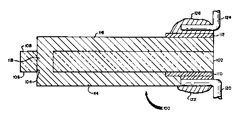
Figure 2 illustrates a cross-section of an
electrical circuit component 100 according to this
invention. An insulative substrate 102 is provided
30 having an aperture 104 extending between first and
second major surfaces 106 and 108 of the substrate.
Metal pad 110 is located on the first major surface of
the substrate. Thick film RAC layers 114 and 116 are
located on the first and second major surfaces of the
substrate. The RAC layer 114 in part overlies the
metal pad 110.. A portion 118 of the composltion
forming the RAC layers extends into the aperture 104
13(~5i2~`9
-15-
connecting the RAC layers on opposite surfaces of the
substrate. A metal lead 120 is bonded to the first
RAC layer and the metal land 110 by solder 122. A
second metal lead 124 is connected to the second RAC
s layer through interposed metal pad 112 by solder 126.
Instead of being soldered the leads can alternatively
be bonded by any other convenient conventional means,
such as ultrasonic wire bonding or thermal compression
bonding.
Although for simplicity in Figure 2 the RAC
layers are shown as forming linear conduction paths,
they can independently form any conduction path
configuration found in conventional circuits. For
example, the conduction path can be serpentine or
15 sinuous. It can be spiral, as in planar motor or
generator windings. Further, instead of itself
providing the entire conduction path between the leads
120 and 124, the RAC layers can form a conduction path
in series and/or in parallel with conventional
20 electrical circuit components, such as resistors,
capacitors, transistors, diodes, integrated circuit
elements, and the like.
The substrate is referred to as insulative,
only because it is insulative in comparison to the
25 contuction properties of the RAC layer. As herein
employet the term "insulative substrate" refers to any
substrate having an electrical resistance of
sufficiently greater magnitude than that of the RAC
layer that current flow occurs predominantly through
30 the RAC layer rather than the substrate on which it is
formed.
While iteal substrates are those which remain
chemically nonreactive turing fabrication of the
crystalline RAC layer, in practice when RAC
35 crystallization temperatures are encountered by the
substrate at least some interaction of the RAC layer
occurs with all but the most stable of substrates. In
,,.
3~ 5
-16-
some instances less than hoped for levels of
electrical conductivity have been observed in
fabricating RAC thin films, believed to be
attributable to interaction of the crystallized RAC
5 layer with its substrate at their mutual interface.
Unwanted reductions in Tc and zero resistivity
temperatures are believed to be unwanted
manifestations of substrate interaction with the
crystalline RAC layer. Performing multiple iterations
10 of the intermediate RAC layer, particularly where the
first intermediate RAC layer forms a thin film, can be
used to control substrate interaction with the thin
film.
It has been observed that the thick films
lS produced by the present process exhibit higher Tc
and superconducting properties with a wider variety of
substrates than has been observed in producing thin
films. In this instance the portion of the
crystalline RAC layer adjacent the substrate is acting
20 as a barrier protecting the portion of the RAC layer
remote from the sub~trate.
An alternative is to interpose between the
substrate and the crystalline RAC layer a barrier of a
different composition. The interposed barrier layer
25 can itself take the form of a crystalline RAC layer,
differing in the specific RAC composition chosen. In
this instance the barrier layer can be viewed as a
second crystalline RAC layer, which can, if desired,
perform electrical conduction a~ well as acting as a
30 barrier. In other instances the barrier can be viewed
as an exten8ion of the 8ub8trate. For example, a
ceramic ~ub8trate coated with a thin refractory metal
layer or a semiconductor substrate coated with an
oxide or nitride, each of which are in turn overcoated
35 with a crystalline RAC layer, can be viewed as an
article having a composite substrate 8upporting a
cry8talline RAC layer or an article having a unitary
.
13(~S2~9
-17-
substrate, a crystalline RAC layer, and an interposed
barrier.
Any rare earth alkaline earth copper oxide
composition known to be convertible to a crystalline
5 phase can be employed in forming the coated articles
of this invention. For example, any of the RAC
compositions disclosed in publications P-l through P-6
can be formed and converted to a crystalline phase by
the process of this invention.
Electrically conductive crystalline RAC
layers can be formed on a wide variety of substrates.
In general any conventional electrical conductor
substrate capable of withstanding processing
temperatures can be employed. For example, metal,
15 glass, ceramic, and semiconductor substrates all
possess sufficient thermal stability to accept
crystalline RAC layers applied by one or more of the
procedures described above. Substrates in both
polycrystalline and monocrystalline form have been
20 successfully employed.
To achieve articles according to this
invention which are not only electrically conductive,
but also exhibit high Tc levels, thereby rendering
them attractive for high conductivity (e.g.,
25 superconducting) electrical applications, it has been
observed that some combinations of substrates and rare
earth al~aline earth copper oxides are particularly
attractive in exhibiting higher Tc levels ant higher
maximum temperatures at which superconductivity is in
30 evitence.
One specifically preferret class of high Tc
articles according to this invention are those in
which the crystalline RAC layer consists of greater
than 45 percent by volume of a rare earth alkaline
35 earth copper oxide which is in a tetragonal K2NiF4
crystalline phase. The K2NiF4 crystalline phase
preferably constitutes at least 70 percent and
~,,
~,
, . . .
,~ ~
~ , .
,
, . . . .
, .
13¢~SZ~;9
--18--
optimally at least 90 percent by volume of the RAC
layer.
A preferred rare earth alkaline earth copper
oxide exhibiting this crystalline phase satisfies the
5 metal ratio:
(I) L2 x:Mx:Cu
where
L is lanthanide,
M is alkaline earth metal, and
x is 0.05 to 0.30.
Among the preferred lanthanides, indicated above,
lanthanum has been particularly investigated and found
to have desirable properties. Preferred alkaline
earth metals are barium and strontium. Optimum
15 results have been observed when x is 0.15 to 0.20.
Thus, in specifically preferred forms of the
invention LBC or LSC layers exhibiting a tetragonal
K2NiF4 crystalline phase are present and capable
of serving high conductivity applications, including
20 those requiring high Tc levels and those requiring
8uperconductivity at temperatures in excess of 10K.
Specific LBC layers in the tetragonal K2NiF4
crystalline phase have been observed to have Tc
levels in excess of 40K.
Another 8pecifically preferred cla88 of high
Tc articles according to this invention are those in
which the crystalline RAC layer consists of greater
than 45 percent by volume of a rare earth alkaline
earth copper oxide which an RlA2C3 crystalline
30 phase, believed to be an orthorhombic Pmm2 or
orthorhombically distorted perovskite crystal phase.
Thi8 pha8e pre$erably constitutes at least 70 percent
by volume of the RAC layer.
A preferred rare earth alkaline earth copper
35 oxide exhibiting this crystalline phase satisfies the
metal ratio:
(II) Y:M2:Cu3
, .
.' " ~ .
~ . .
.
13~52~
-19-
where
M is barium, optionally in combination with one or
both of strontium and calcium.
Although the RlA2C3 crystalline phase
5 by its crystal lattice requirements permits only a
specific ratio of metals to be pre~ent, in practice
differing ratios of yttrium, rare earth, and copper
are permissible. The metal in excess of that required
for the RlA2C3 crystalline phase is excluded
10 from that phase, but remains in the YAC layer. This
is further illustrated in the examples below.
Alkaline earth oxides constitute a preferred
class of substrate materials. They are in ~eneral
relatively inert, refractory materials which exhibit
15 limited interaction with the RAC layers during their
formation. Magneæia in either monocrystalline (i.e.,
periclase) or polycrystalline form constitutes a
particularly preferred substrate material because of
its low level of interaction with the RAC layer.
20 Strontium titanate, because it can be readily formed
in a perovskite crystalline form, constitutes another
preferred alkaline earth oxide substrate material.
Alumina, either in monocrystalline form
(i.e., 8apphire) or in polycrystalline form
25 constitutes another preferred clas8 of substrate
materials. Polycrystalline alumina because of its
ready availability and general use as an electrical
circuit substrate material is a particularly preferred
substrate material. Aluminum nitride is also
30 contemplated as a substrate material.
Semiconductor wafers, particularly
monocrystalline silicon and III-V compound wafers,
also constitute useful classes of substrates for the
-~ articles of this invention.
Another specifically contemplated class of
sub~trate materials are refractory metals. Such
metals are, of course, well suited to withstanding RAC
~' ' . ' .
13~S;~5;9
-20-
layer crystallization temperatures of 1000C or more.
Refractory metals such as tungsten, tantalum,
titanium, and zirconium are particularly
contemplated. The refractory metal can form the
5 entire substrate or a thermally resistant layer onto
which the RAC layer is coated.
Although some interaction between substrate
materials and a contiguous RAC layer is believed to
occur when the article is heated to temperatures above
10 about 9000C, interaction effects can be minimized by
employing the interposed barrier formation techniques,
described above. Further, the laying down of thick
films has been found to minimize unwanted substrate
interaction effects.
The ligands present in the metal-ligand
compounds described above form no part of the final
article and therefore can be chosen based solely upon
convenience in performing the process steps described
above. Ligands are chosen first of all for their
20 ability to form solutions in which rare earth,
alkaline earth, and copper combined with the ligands
are each soluble in the desired proportions. Second,
the ligands are chosen to be volatilizable during
heating to form the intermediate ~AC layer.
By ~volatilizable~ it is meant that the
ligand or its component elements other than oxygen can
be removet from the substrate surface at temperatures
below the crystallization temperature of the RAC layer.
Inorganic ligands, such as nitrate, sulfate,
30 and halide ligands, are illustrative of preferred
ligands satisfying the criteria set forth above.
Nitrate, bromide, and chloride ligants are
particularly preferred. In general the ligands are
chosen 80 that each of the rare earth, alkaline earth,
35 and copper ligand compound~ exhibit approximately
similar solubility characteristics.
.,
,;
,. ...
j, . . .
:,...
,,
,......................................................................... .
. . , .. :
-
13C) 52~
-21-
Any evaporative solvent for the metal-ligand
compounds can be employed for particle fabrication.
Again, the solvent forms no part of the final
article. Polar solvents, such as water or alcohols
(e.g., methanol, ethanol, propanol, etc.), are
particularly suited for use with metal-ligand
compounds containing the inorganic ligands noted above.
Where a paste is coated, the paste contains
either a small residual portion of the original
10 solvent for the metal-ligand compounds or a different
liquid to promote cohesion. The liquid fraction of
the paste must be volatilizable. The evaporative
solvents noted above all satisfy this criteria.
The paste apart from the metal-ligand
15 particles can be identical in composition to
conventional inks employed in screen printing. Screen
printing inks normally contain an active ingredient
(in this instance supplied by the metal-ligand
particles), binders to promote substrate adhesion
(~uch as glass frit or crystalline oxide powder),
screening agents used to enhance the rheological
properties of the ink -usually a higher molecular
weight polymer, such as poly(vinyl alcohol) or
poly(ethylene glycol), and a liquid, most commonly
25 water or an alcohol. It is a particular advantage of
this invention that the metal-ligand particles and
liquid together provide excellent rheological and
adhe~ion properties without the necessity of
incorporating other screen printing ink ingredients.
Proce3sing temperatures employed in forming
the intermediate RAC layers and in subsequently
converting the intermediate layers to electrically
conductive crystalline layers can vary significantly,
depending upon the specific RAC composition and
35 crystal form under consideration. Crystallization is
in all instances achieved below the melting point of
the RAC composition. Melting points for RAC
l3as~
compositions vary, but are typically well above
1000C. Typically the electrically conductive
crystalline RAC layers are formed by heating to
temperatures in the range of from about 900 to 1100C.
The metal-ligand compounds can be in
crystalline form. Since the metal-ligand compounds
are confined to separate particles at the time
precipitation from solution occurs, undesirable phase
separation of the differing metal components is
10 effectively confined within the individual particle
boundaries. Thus, simple inorganic ligands that favor
deposition of the metal-ligand compounds in
crystalline form are entirely compatible with the
practice of this invention.
A preferred technique for producing a high
Tc coating employing an intermediate layer of the
LAC composition metal ratio I above, particularly an
LBC or LSC composition, is to heat the intermediate
layer on the substrate to a temperature of about 925
20 to 975C and then increase the temperature to about
975 to 1050C. Following conversion of the LAC layer
to the tetragonal K2NiF4 crystalline phase, it is
cooled slowly at rate of of 25C or less per minute
until it reaches a temperature of 550 to 450C. The
25 LAC layer is then held at this temperature or reheated
to this temperature in the presence of an oxygen
atmosphere until oxygen eguilibration is substantially
complete, typically about 20 to 120 minutes.
A preferred technigue for producing a high
30 Tc coating employing an intermediate layer of the
YAC composition satisfying metal ratio II above,
particularly YBC, is to heat the intermediate layer on
the substrate to a temperature greater than 900C, but
less than 950C, optimally 920 to 930C. Following
35 conversion of the intermediate layer to the
RlA2C3 crystalline phase, it is cooled 810wly at
rate of of 25C or less per minute until it reaches a
~ ' ' ~ ' '
.
~3~JS2~9
temperature of 750 to 400C. The YAC layer is then
held at this temperature or reheated to this
temperature following cooling in the presence of an
oxygen atmosphere until oxygen equilibration is
5 substantially complete, typically about 20 to 120
minutes.
Thick films produced by the present invention
can vary widely in their thicknesses. Final
thicknesses are contemplated in the range of from
10 about 5 to 200 ~m, with thicknesses of about 10 to
100 ~m being preferred for most thick film
applications. With care to avoid thermal stresses
still greater coating thicknesses should be possible.
As previously noted thin films can be readily
15 fabricated by the process of this invention.
~s
Details of the preparation and performance of
articles according to this invention are illustrated
by the following examples.
20 Example 1
This example illustrate~ the formation of a
conductive thick film coating of YlB2C3 on
sapphire.
' ~E~=l
A particle-forming solution was prepared by
mixing the following ingredients in the proportions
indicated, corresponding to the cation ratio in
- YlB2C3:
Y(N03)36H20 13.41 g
30 Ba(N03)2 18.30 g
CU(N3)22'5H2 24.42 g
H20 500.00 ml.
The water employed was distilled water. The 801ution
was filtered through a 0.45 ~m membrane filter.
PFS-l was converted to a mixed powder and
paste by spray drying. A Yamato Model GA-31 spray
drier was employed in its normal mode of operation.
,
'
, ~
:
13(15Z~9
-24-
Inlet Temp. 200C
Outlet Temp. 80OC
Aspirator Setting 2.5
Pump Setting 2.5
Drying Air0.3-0.35 m3/min.
Atomizing Air O.53 MPa
Pulsed Air Interval10 sec.
A #2050SS liquid nozzle and a #64-5SS air nozzle were
used. The spraying rate was about 10 ml/min.
The material obtained from the spray drier
was a mixture of a dry powder (pale blue) and a
partially hydrated powder which was a thick paste (sky
blue). Addition of approximately 10% by weight water
transformed the dry powder into a paste. Chemical
15 analysis indicated the cation ratio to be identical to
that of the starting solution.
The paste was spread onto a monocrystalline
alumina (sapphire) 1102 crystal surface. Paste
coating thicknesses were in the 10 to 20 ~m range.
The pa8te was heated to 925C on the
sub8trate in air in a furnace and held at that
temperature for 5 minutes. At the end of 5 minutes
the coated article was allowed to cool at the rate of
<25C per minute.
The resulting YBC crystalline layer was about
14 ~m in thickness and adhered well to the
substrate. Sheet resistance of the YBC crystalline
layer was determined to be in the order of 20 to 40
ohms per sguare at room temperature. X-ray analysis
30 confirmed that the YBC crystalline layer exhibited a
YlB2C3 pha8e-
This example illustrates the formation of a
high transition temperature superconductive thick film
35 coating of YlB2C3 on monocrystalline MgO.
PFS-2
A particle-forming solution was prepared by
' mixing the following ingredients in the proportions
,~ i
'
,. . .
",", ., ....................... , ' .:
. - ' ,
13(152~i9
-25-
indicated:
Y(NO3)36H2O28.15 g
Ba(NO3)236.6 g
Cu(N03)22.5H20 51.29 g
H2O 750 ml.
The water employed was distilled water. The solution
was filtered through a 0.45 ~m membrane filter. To
compensate for possible loss of the yttrium and copper
salts a 5/O molar excess of each was employed above the
10 desired YlB2C3 stoichiometric molar ratio.
Subsequent investigations have shown that no
significant loss of either yttrium or copper salts
occurs. Therefore, a stoichiometric excess of these
salts as been shown not to be necessary but
15 nonetheless useful.
PFS-2 was converted to a dry powder by spray
drying, using the same spray drier and nozzles as in
Example 1.
Inlet Temp. 200C
Outlet Temp. 100-105C
Aspirator Setting 3
Pump Setting 4
Drying Air0.3-0.35 m3/min.
Atomizing Air 0.30 MPa
Pulsed Air Interval20 sec.
The same nozzles and spraying rate were
employed as in Example 1.
The powder obtained from the spray drier very
dry and was stored briefly in a vacuum oven before use.
A small amount of the powder was mixed with
water in the amount of 1 to 2 drops of water per gram
of powder to form a paste. The paste was then hand
coated on a monocry8tlline MgO substrate to a
thickne~s of approximately 50 ~m.
The coated substrate was placed on a hot
plate at room temperature and heated rapidly to 535C,
at which time it was covered with aluminum foil.
,
- 13~52~
-26-
Heating was continued for approximately 30 minutes, at
the end of which time the temperature of the coating
was in the range of from 590 to 650C. The sample was
allowed to cool under the aluminum foil until it
5 reached about 250C and was then taken off the hot
plate. It was then cooled further to room temperature
at a relatively rapid rate.
The sample was next heated to 925C in air in
a furnace and held at that temperature for 15
10 minutes. At the end of 15 minutes the sample was
allowed to cool to room temperature at the rate of
less than 10C per minute.
The resulting YBC crystalline thick film
adhered well to the substrate. X-ray analysis
15 indicated the orthorhombic YlB2C3 phase, with a
small amount of other phases being present. The
secondary phases appeared as green blotches on the
surface of the black sample. There were some cracks
in the coating.
The sample was then oxygen annealed by being
held at 650C for 30 minutes in an oxygen atmosphere
and then cooled in the oxygen atmosphere to about
290C over a period of 32 minutes.
The sheet resistance of the sample at room
25 temperature before and after oxygen annealing was 3
ohms per square, measured with a ~our point probe.
The sample was cooled with its resistance
being concurrently measured. The resistance remained
constant until the region of 95 to 100K was reached.
30 At 77K+2K the sample was entirely superconduct-
ing. Remeasurement determined Tc to be 97K~2K
with superconductivity occurring at 76K~2K.
~$~mple 3
This example illustrates screen printing of
35 patterned coatings.
PFS-3
A particle-forming solution was prepared by
mixing the following ingredients in the proportions
,~, .. .. ...
13(~52~9
--27--
indicated:
Y(N03)36H2026.81 g
Ba(N03)2 36.59 g
CU(N3)22'5H2 48.85 g
H20 690 ml.
~ Preparation was similar PFS-2, except that no
stoichiometric excess of metal salts was included.
PFS-3 was converted to a wet powder by spray
drying, using the same spray drier and nozzles as in
10 Example 1.
Inlet Temp. 180-200C
Outlet Temp. 75-850C
Aspirator Setting 3 (approx.)
Pump Setting 1.5
Drying Air 0.3-0.35 m3/min.
Atomizing Air O.30-0.34 MPa
Pulsed Air Interval 20 sec.
The same nozzles and spraying rate were
employed as in Example 1.
The wet powder obtained was placed in a
drying oven at 110C for several days. It was removed
and ground using a mortar and pestle. The powder was
then converted to a paste by adding approximately 13%
by weight water dropwise until a thick consistency was
25 obtained. A portion of the paste was then further
diluted to approximately 14% by weight water to give a
thinner consistency paste, The two pastes are
identified as the diluted and non-diluted pastes.
One sample of the diluted paste was coated
30 onto a polycrystalline alumina insulative support
having a gold contact pattern on its surface. The
diluted paste was coated 80 that it overlapped both
areas containing the gold contact pattern and defined
areas between spaced gold contact areas. The diluted
35 paste was screen printed in a series of parallel
rectangular patterns of varied size using a 200 mesh
screen.
,,, ~,,,
13~5Z~g
-28-
After a 15 to 20 minute delay the sample
coated as described above was heated on a hot plate as
described in Example 2. The sample was heated in air
in a furnace at 8500C for 15 minutes and then cooled
5 at a rate of less than 250C per minute to room
temperature.
Some cracking of the coating was observed,
however resistance probes to spaced gold contact areas
joined by the coating demonstrated that the coating
10 provided an electrical conduction path. The final
coating was about 24 ~m in thickness.
Several more samples processed as described
above through the hot plate stage were furnace heated
and cooled under varied conditions. Both the diluted
15 and non-diluted paste appeared capable of producing
desirable coatings. Higher furnace temperatures and
more abrupt changes in temperatures increased the
number of cracks observed, but in each instance
patterned electrical conductors were obtained. In
20 every in~tance the gold contact pattern produced
satisfactory conductive contact with the YBC layer.
Example 4
This example illustrates coating on
polycrystalline alumina and strontium titanate
Z5 substrates.
A powder was made from a solution similar to
PFS-l, except it was 50 ml more concentrated by using
the spray drying conditions of Example 2. Using
procedures similar to those described in Example 2
30 coatings were prepared on alumina ant strontium
titanate supports. The coating thickness after hot
plate treatment of the alumina substrate article was
40 to 70 ~m. The coating thickness on one portion
of the strontium titanate article was 90 to 100 ~m
35 and 40 to 60 ~m on a second portion.
The samples were heated in air in a furnace
at 925C for 5 minutes, cooled to room temperature at
''.'
-~'
,. . .
,. . .. ....... . .
,:
,
:
~3~S2~9
-29-
a rate of less than 25OC per minute, heated at the
rate of 25 to 50OC per minute to 925OC, held at that
temperature for 20 minutes, and then cooled back to
room temperature at same rate indicated above. The
5 final coating thicknesses were found to be about half
~ the thicknesses noted above.
After annealing the samples at 925C in
oxygen, the strontium titanate sample exhibited a
sheet resistance of 5 ohms per square while the
10 alumina sample exhibited a sheet resistance of 50 ohms
per square at room temperature.
Example 5
This example illustrates forming conduction
paths through apertures in a substrate.
A polycrystalline alumina substrate was
employed having a thickness of about 1 mm containing
five apertures of 0.5 mm in diameter spaced about 1 mm
apart.
A coating was prepared on one surface of the
20 substrate by the same procedure described in Example 2
through the step of cooling to room temperature
following hot plate heating, except that PFS-4 was
substituted for PFS-2 and the spray drier was operated
under the conditions indicated below:
25 F~-4
Y(N03)36H20 40.22 g
Ba(N03)2 54.88 g
Cu(N03)22.5H20 73.27 g
H20 1400.00 ml.
Inlet Temp. 200C
Outlet Temp. 90-95C
Aspirator Setting 3.1
Pump Setting 1.7
Drying Air 0.3-0.35 m3/min.
Atomizing Air 0.1 MPa
Pulsed Air Interval20 sec.
The paste produced contained 9.3% by weight water.
. ~, ..... .
13~52~9
-30-
The opposite major surface of the substrate
was then similarly coated and processed, except that
the substrate was not placed directly on the hot
plate, but was sat on spaced pieces of 1 mm
5 polycrystalline alumina with the first coating being
closest located nearest to the hot plate surface.
Following hot plate cooling the article with
coatings on opposite major surfaces was placed in a
furnace again using the spaced pieces of
10 polycrystalline alumina and further processed as
described in Example 2. The first YBC film was 10
~m in thickness while the second YBC film was 30
~m in thickness.
By applying electrical probes to the first
15 and second surfaces it was determined that electrical
~ conduction paths through the apertures had been
; established. No current conduction occurred when
either or both probes were placed on uncoated
substrate surfaces adjacent to the YBC film.
The invention has been described in detail
with particular reference to preferred embodiments
~ thereof, but it will be understood that variations and
'~, modifications can be effected within the spir~it and
scope of the invention.
". 25
.
~,.
' :,
i ~1
, 35
,.,~ 'i
,,, I
v
,...
?~
i,~.'' :
',.,~,:
~. ' - , -
r' " '
i, .
'~
. : .'