Note : Les descriptions sont présentées dans la langue officielle dans laquelle elles ont été soumises.
RD-16,737
13(~
METHOD FOR PRODUCING HIGH YIELD ELECTRICAL
CONTACTS TO N AMORPHOUS SILICON
Backqround of the Disclosure
The present invention is generally directed to a
method for treating a doped amorphous silicon surface to
enhance electrical contact. The method is applicable to the
production of microelectronic circuit devices, and more
particularly, is more applicable to the production of thin
film amorphous silicon semiconductors, particularly those
employed in liquid crystal display matrix addressed systems.
A liquid crystal display device typically com-
prises a pair of flat panels sealed at their outer edges and
containing a quantity of liquid crystal material. The flat
panels generally possess transparent electrode material
disposed on the inner surfaces in predetermined patterns.
One panel is often covered completely by a single
transparent ground plane electrode. The opposite panel is
configured with an array of transparent electrodes, referred
to herein as pixel (picture element) electrodes. Thus a
typical cell in a liquid crystal display includes lig~id
crystal material clisposed between a pixel electrode and a
ground electrode forming, in effect, a capacitor-like
2~ structure dicposed between transparent front and back
panels. In general, however, transparency is reguired for
only one of the two panels and the electrodes disposed
thereon.
In operation, the orientation of liquid crystal
material i5 effected by voltages applied across the elec-
trodes on either side of the liquid crystal material.
Typically, voltage applied at the pixel electrode effects a
change in the optical properties of the liquid crystal
material. This optical change causes the display of
RD-16,737
13~3~
information on the display screen. In conventional digital
watch displays and in new LCD displays, screens used in some
miniature television receivers, the visual effect is
typically produced by variations in reflected light.
However, the utilization of transparent front and back
panels and transparent electrodes also the permits the
visual effects to be produced by transmissive effects.
These transmissive effects may be facilitated by
subsequently powered light sources for the display including
fluorescent type devices. This is typically referred to as
back lighting. Various electrical mechanisms are employed
to sequentially turn on and off individual pixel elements in
an LCD display. Most relevantly, the switch element of the
present invention comprises a thin film field effect
transistor employing a layer of amorphous silicon. These
devices are preferred in many LCD devices because of their
potentially small size, low power consumption, switching
speed, ease of fabrication, and compatibility with
conventional LCD structures.
Thin film field effect transistors made from
plasma enhanced chemically vapor deposited (PECVD) amorphous
silicon ta-Si) and silicon nitride are ideal for matrix
addressing of liquid crystal displays. They are fabricated
on glass substrates with high picture element density using
methods and equipment employed in conventional integrated
circuit fabrication. In one process for FET fabrication and
LCD displays, a molybdenum contact is made to N amorphous
silicon using two masking steps. After a deposition of an
insulative material such as silicon nitride, a layer of
intrinsic amorphous silicon and the doping of the upper
portions of the amorphous silicon layer, a thin layer of
molybdenum is sputter deposited. This film is patterned
back into small regions called mesas. Then the silicon
RD-16,737
~3(~
nitride/silicon layers are patterned into regions somewhat
larger than the mesas and referred to herein as islands.
Subsequently, thick molybdenum is deposited on the wafer and
patterned into source/drain and data line electrodes. The
deposition of the thin molybdenum before subsequent process-
ing into islands has been found to be necessary to ensure
re~liable contact of molybdenum to the N silicon. Hence, it
is seen that two masking steps are required to form the
contact: the mesa and mask and the island mask. Reducing
the number of masking steps is desirable because it reduces
processing time and in general, increases device yield.
Summary of the Invention
In accordance with a preferred embodiment of the
present invention, a thin layer of molybdenum, about 50
nanometers in thickness, is sputter deposited on the N
silicon. This molybdenum layer is then removed by etching
without any patterning required. The silicon/silicon
nitride layer is then patterned into islands as before.
Then molybdenum source/drain metal is deposited, patterned
and etched and the process is completed. It is the deposi-
tion of this thin molybdenum layer and its subsequent
removal which is believed responsible for the improvements
in electrical contact between the molybdenum source/drain
electrodes and the N amorphous silicon material.
It is noted that the preRent method of processing
eliminates the need to form molybdenum mesas prior to
formation of the source/drain contacts. Thus one masking
step is eliminated. It is also noted that, without the
present invention, the mesa/island structure is generally
required since the overhang problem due to undercutting ofthe silicon/silicon nitride layers can develop and cause
step coverage problems for the source/drain metallization.
RD-16,737
13(~S3~8
Accordingly, it is an object of the present
invention to provide a method for improving electrical
contact to amorphous silicon materials. It is also an
object of the present invention to reduce the number of
mas~ing steps re~uired in the formation of amorphous silicon
thin film transistors.
It is yet another object of the present invention
to increase the yield of thin film field effect transistor
devices employed in microcircuit applications.
It is yet another object of the present invention
to reduce the number of masking steps and improve the yield
in the manufacture of matrix addressed liquid crystal
displays.
Lastly, but not limited hereto, it is an object of
the present invention to provide a method for treating an
amorphous silicon surface, particularly an N doped amor-
phous silicon surface, to enhance electrical contact with
said surface, particularly when the subse~uent contacting
material is molybdenum.
Descri~tion of the Fiqures
The subject matter which is regarded as the
invention is particularly pointed out and distinctly claimed
in the concluding portion of the specification. The inven-
tion, however, both as to organization and method o prac-
tice, together with urther objects and advantages thereo,
may best be understood by reference to the following
description taken in connection with the accompanying
drawings in which:
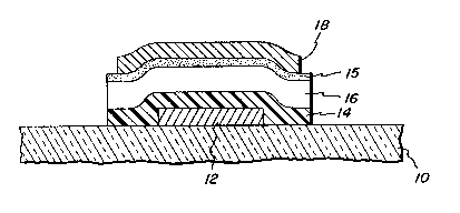
Figure lA is a cross-sectional side elevation view
illustrating the mesa and island structures present at one
staqe in thin film FET fabrication;
RD-16,737
~3(~53~8
Figure lB is a cross-sectional side elevation view
similar to Figure lA, but more particularly illustrating the
deposition of source/drain contact material and the etching
of a gap therein to form an inverted field effect transistor
device;
Figure 2A is a cross-sectional side elevation view
illustrating an initial process step in accordance with the
present invention;
Figure 2B is similar to Figure 2A, but more
particularly illustrates the removal of the thin layer of
deposited molybdenum resulting in permanent alternation of
the N amorphous silicon surface;
Figure 2C is similar to Figure 2B, but more
- particularly illustrates patterning via a mask step to form
islands and particularly illustrating the absence of mesa
structures;
Figure 2D is similar to Figure 2C, but more
particularly indicating the deposition and patterning of
source/drain metallization.
Detailed Description of the Invention
Figures lA and lB are provided to particularly
illustrate the fact that the present invention utilizes one
less masking step than is provided by other processing
methods. In particular, Figure lA illustrates one stage in
the fabrication of an inverted, thin film field effect
transistor. Figure lB illustrates a completed FET structure
produced in accordance a process which is different than the
present invention. The transistor structures shown in
Figure 1 are seen as being disposed upon a glass substrate
10. This is the typical situation in which these transis-
tors are employed in liquid crystal display devices.
However, in general, any insulative substrate material which
RD-16,737
13~S3~8
is thermally compatible and non-reactive with other mate-
rials employed in the transistor is suitable for use as a
substrate. It is also noted that the transistor structureS
as illustrated in the figures herein are referred to as
inverted since the gate electrode is deposited at a lower
point in the transistor structure.
In particular, Figure lA illustrates gate elec-
trode 12 disposed on substrate 10. The disposition of gate
electrode materials and conductive leads typically requires
a separate masking and patterning step which is not specifi-
cally relevant to the practice of the present invention.
However, following formation of metallic gate electrode
patterns 12, insulative layer 14, typically comprising
silicon nitride is deposited over the substrate. In a
similar fashion, a layer of amorphous silicon material 16 is
then deposited over insulative layer 14. Doped amorphous
silicon layer 15 is then deposited in a conventional fashion
using well known methods to produce layer 15 of doped N
amorphous silicon. Next, a layer of metallic material 18
such as molybdenum is employed. Molybdenum layer 18 is
employed for the purpose of enhancing electrical contact to
the doped N a~orphous silicon material 15. It is the
improvement of this electrical contact to which the present
invention is specifically addressed. In accordance with the
process illustrated in Figures lA and lB, layer 18 is
subject to a masking and patterning operation resulting in
the formation of a mesa structure 18 shown in Figure lA. It
is noted that this particular masking step is the one which
is eliminated by the practice of the present invention.
Nonetheless, in the process illustrated, a subsequent ~
patterning and masking operation removes portions of layers
14, 15 and 16 so as to form island structures beneath the
mesa structure shown. It is noted that if layer 18 is not
RD-16,737
13(~53~
removed or cut back into mesas prior to deposition and
etching of source and drain electrode material, an overhang
due to undercutting of the silicon/silicon nitride material
is apt to develop and to cause step coverage problems for
the source/drain metallization layer. Thus, the separate
masking operations for mesa and island structures have been
found to be highly desirable to prevent step coverage
problems from occurring.
Figure lB illustrates the completion of a process
for forming a thin film field effect transistor from the
structure seen in Figure lA. In particular, a layer of
conductive material 19, preferably comprising molybdenum is
deposited and patterned as shown. In particular, patterning
-- of the molybdenum material results in the formation of an
aperture or gap which separates source and drain portions of
the field effect transistor. It is noted that contact
improvement layer 18 is divided into portions 18' as shown.
While typically comprising the same material, preferably
molybdenum, structures 18' and 19 are shown as distinct in
Figure lB since the structures actually perform somewhat
different functions. In particular, as noted above, molyb-
denum layer 18 (also designated as 18' after patterning) is
relatively thin, namely approximately 50 nm, and serves
solely to improve electrical contact to the doped amorphous
silicon layer 15. However, a much thicker metallization
layer 19 is actually employed to provide source and drain
metallization patterning and connection of these device
elements to the rest of the circuit. In general, in a
liquid crystal display type device as described above, each
pixel element is associated with a single FET device such as
that shown in Figure lB (or in Figure 2D as is more
particularly discussed below with reference to the process
of the present invention). It is also noted that the
~3~53~8 RD-16,737
figure of the present invention are not shown to scale and,
in particular, the dimensions in the vertical direction have
been exagger~ted so as to more readily provide a pictorial
illustration of the invention and also to provide drawings
which are more readily understood by those skilled in the
microelectronic fabrication arts.
A process for carrying out the present invention is
particularly illustrated in Figures 2A-2D. The processing
required to produce the cross-section in Figure 2A is
typically the same processing that is employed in the
construction of the device stage shown in Figure lA, as
discussed above, up to and including the formation of doped
amorphous silicon layer 15. In this regard, it is noted
that while the doped region herein is referred to as a
separate layer lS, it is nonetheless understood by those
skilled in that art that this layer is actually formed by
doping a portion of amorphous silicon layer 16 and as such,
layers 15 and 16 essentially form a single structure with
the exception that the uppermost regions of the amorphous
silicon material are doped with a particular polarity dopant
such as phosphorus.
However, Figure 2A illustrates the deposition of
a thin layer of molybdenum which is preferably sputtered
onto the N+ doped amorphous silicon. This layer of
molybdenum 21 is preferably approximately 50 nanometers
in thickness but may range from about 10 to 100
nanometers. It is preferably deposited by sputtering,
also, in marked contrast to other process, thin
molybdenum layer 21 is removed. It is preferably removed
by etching with a mixture of phosphoric acetic, and
nitric acids in an aqueous solution. This is typically
referred to as a PAWN etch. Most importantly, it is
noted that molybdenum layer 21 is removed without any
patterning step being employed. This is in marked
contrast to the process illustrated in Figures lA and
RD-16,737
~3(I53~3
lB. As a result of the deposition and removal of molybdenum
layer 21, it is believed that a permanent alteration of N
doped amorphous silicon layer 15 is produced. This
alteration is illustrated by heavy line 20 seen in Figures
2B, 2C and 2D. It is this permanent alteration which
appears to produce the desirable characteristics of the
present invention. In accordance with preferred embodiments
of the present invention for forming thin film field effect
transistors, the silicon/silicon nitride layer is then
patterned into islands as described above. A typical
resulting island is shown in Figure 2C. It is particularly
noted that mesa structures are absent in Figures 2C and 2D
and that no problem of undercutting, overhanging or step
coverage is present. Nonetheless, the alteration of the
surface of N doped amorphous silicon 15 renders that
surface much more susceptible to electrical contact with
subsequently deposited molybdenum material 19 which is
patterned as described above to produce source and drain
metallization. The resulting structure is seen in Figure
2D. It has been found that if the deposition of molybdenum
layer 21 is omitted from the process, the yield of good
electrical contacts is significantly reduced. It is also
noted that experiments conducted clearly indicate that it is
the deposition and subse~uent removal of molybdenum layer 21
which results in the beneficial effects provided by the
process of the present invention. In particular, it has
been determined by electrical measurements that there is an
alteration of the N silicon surface due to the deposition
and removal of the molybdenum. Even after long etching in a
PAWN etch to remove the molybdenum, the electrical
conductivity of the N silicon is much higher than for
untreated N silicon. Furthermore, sputter etching of the
surface, followed by plasma etching sufficient to remove a
RD-16,737
13~3~1~
small fraction of the N material, results in a dramatic
reduction of the N conductivity in comparison with that
observed from material exposed to molybdenum deposition and
removal. This indicates that a permanent alteration of the
N surface has occurred. This alteration persists even
through multiple resist processing steps including cleaning
steps and oxygen ashing. This altered surface is important
for producing a good bond and contact between the thick
molybdenum layer 19 which is deposited and patterned into
source and drain metallization after formation of the
islands.
- In an alternate embodiment the first molybdenum
cap is not removed until just prior to deposition of the
source-drain metalization. This molybdenum cap protects the
surface from contamination during intermediate processing
steps such as IT0 deposition and patterning. Subsequent
etching of the molybdenum cap is also advantageous in that
it strips the Si surface of the contaminants.
Accordingly, from the above, it should be appreci-
ated that the process of the present invention significantlyimproves contact to doped amorphous silicon surfaces. It is
further seen that the process of the present invention
reduces the number of masking steps employed in the fabrica-
tion of thin film amorphous transistors. It is also seen
that the process described herein is particularly advanta-
geous for forming FET control device in matrix addressed
liquid crystal displays. It is also seen that the process-
ing time and the device yield associated with fabrication of
such transistors is also improved by the process of the
present invention.
While the invention has been described in detail
herein in accord with certain preferred embodiments thereof,
many modifications and changes therein may be effected by
RD-16,737
13~i3~3
those skilled in the art. Accordingly, it is intended by
the appended claims to cover all such modifications and
changes as fall within the true spirit and scope of the
invention.