Note : Les descriptions sont présentées dans la langue officielle dans laquelle elles ont été soumises.
13~6S3~;
-1 -
A VIDEO SIGNAL PROCESSING APPARATUS
BACKGROUND OF THE INVENTION
This invention relates generally to a video signal processing
apparatus and more particularly, the invention relates to a video signal
processing apparatus for reproducing luminance and color difference signals
from a video si~nal including a time-compressed luminance and color difference
si~nals in one horizontal scanning line interval, their time-compressed factors
being different from each other.
A video signal processing apparatus is used for reproducing
luminance and color difference signals from a time-division-multiplexed video
signal including a time-compressed luminance and color difference signals by
time-expansion. Such a video signal is employed in MAC (Multiplexed Analog
Components), TCI (Time Compressed Insertion) systems, and other systems
using time-division-multiplexed video signal.
The object and features of the present invention will become more
readily apparent from the following detailed description taken in conjunction
with the accompanying drawings in which:
Fig. 1 is a block diagram of an embodiment of the invention;
Fig. 2 is a block diagram of a signal generation circuit of Fig. 1;
Figs. 3 and 4 are illustrations for illustrating component signals of
video signals MAC and TCI systems respectively;
Fig. 5 is a timing chart of signals processed in the circuit of Fig.
1;
Figs. 6, 7, and 8 show modified circuit arrangements of the
embodiment of Fig. 1; and
Fig. 9 is a block diagram of a video signal processing circuit of
prior art.
The same or corresponding elements or parts are designated at
like references throughout the drawings.
Fig. 3 shows an MAC system video signal. In Fig. 3, block 1
includes synchronizing and da~a signals; block 2, a color difference signal
which is time-compressed by 1/3; and block 3, a luminance signal which is
time-compressed by 2/3. These signals are transmitted for 1 H (one horizontal
C
-2- 1306536
scannin~ interval~. Fig. 4 shows a TCI system video signal. In Fi~. ~, block
21 includes synchronizing and data signals; block 22, a color difference signal
which is time-compressed by 114; and block 23, a luminance signal which is
time-compressed by 1. These signals are transmitted for 1 H.
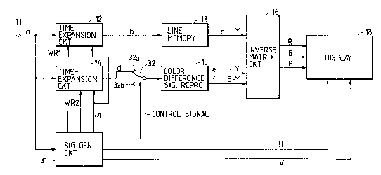
A prior art video processing circuit is shown in Fig. 9 of a block
diagram. In Fig. 9, an inpu~ video signal "a" is applied to an input terminal 11and is sent to a time-expansion circui~ 12, a time-expansion circuit 14, and a
signal generation circuit 17. ~he time-expansion circuit 12 expands a
luminance signal of the video signal "a" by an expansion ratio of three to
reproduce a luminance signal with respect to time base. The time-expansion
circuit 14 exp~nds a color difference signal of the video signal "a" by an
expansion ratio of 3/2 to reproduce a color difference signal with respect to
time base. Time-expanded signals "b" and "d" are sent to an inverse matrix
circuit 16 through a line memory 13 and a color difference signal reproduction
circuit 15 respectively. The line memory 13 adjusts timing relation between
these video signals. The color difference signal reproduction circuit 15
reproduces simultaneously two color difference signals from two successive
horizontal scanning lines of the signal "d". The inverse matrix circuit 16
produces primary color signals R, G, and B sent to a display 18. The
time-expansion circuits 12 and 14 are controlled by clocks from a signal
generating circuit 17 which generates clock signals by an unshown
phase-locked loop circuit responsive to a horizontal synchronizing pulse
detected from the input video signal.
As mentioned above, the prior art video processing apparatus
reproduces a video signal from time-compressed video signals. However, there
is a drawback that when an output signal of the phase-locked loop circuit (PLL)
of the signal generation circuit 17 is out of phase with its input signal, i.e., not
locked, the time-expanded luminance signal becomes out of phase with the
time-expanded color difference signal because time expansion ratios of the
30 time-expansion circuits 12 and 14 are different therebetween. Therefore, there
are two types of disturbed images, i.e., color and luminance images on the
display 18 when the PLL is not locked. Such a disturbed color image over the
disturbed luminance image gives a viewer unpleasant feeling. In other words,
3 1306536
a reproduced video ima~e on the display 18 has a double image of luminance
and color images when the PLL is not locked.
SUMMARY OF T~IE INVENTiON
The present invention has been developed in order to remove the
above-described drawbacks inherent to the conventional video processing
apparatus .
According to the present invention there is providecl a video signal
processing apparatus for processing a video signal including synchronizing
pulses, a time-compressed color difference and luminance signals, compression
factors of those signals being different from each other, the color difference
signal and luminance signals being transmitted sequentially for one horizontal
line for simultaneously outputting time-reproduced color difference and
luminance signals, comprises: first and second time-expansion circuits for
producing the time-reproduced luminance and color difference signals in
response to first and second clocks respectively; a switching circuit for
sel~ctively outputting the time-reproduced color difference signal in response
to a control signal; a PLL responsive to the video signal including a frequency
dividing circuit for produciny the first and second clocks, and a synthesized
synchronizing pulse; and a phase detecting circuit for detecting a phase relation
between the video signal and the synthesized synchronizing pulse to produce
the control signal. When the PLL is out of phase with the synchronizing pulse,
i.e., not locked, the switch does not transfer the color difference signal from
the second time-expansion circuit, preventing time-reproduced signals from
producing a double image on a display.
The control signal can also be obtained from a phase detector
included in the PLL.
Referring now to the drawings, Fig. 1 is a block diagram of a
vid00 processing apparatus of an embodiment according to the invention.
In Fig. 1, an input video signal "a" of MAC system is applied to
an input terminal 11 and is sent to a time-expansion circuit 12, a
time-expansion circuit 14, and a signal generation circuit 31. The
time-expansion circuit 12 expands the signal "a" with respect to time base by
an expansion ratio of "3/2" to reproduce a luminance signal in response to a
write clock WF~1 and a read clock RD from the signal generation circuit 31.
r~
~' .
4 1306s36
Actually, the time-expansion circuit 12 is a digital memory which stores its
input data in response to the write clock WR1 and outputs the stored data in
response to the read clock RD. The tirne-expansion circuit 14 expands the
signal "a" by an expansion ratio of three to reproduce a color difference signalwith respect to time base in response to write clock WR2 and the read clock
~1~ from the signal generation circuit 31. Actually, the time-expansion circuit
12 is a digital memory which stores its input data in response to the write
clock WR1 and outputs the stored data in response to the read clock RD. An
output signal "b" from the time-expansion circuit 12 is sent to a line memory
13 delaying the signal "b" and outputting a signal "c" for the subsequent
horizontal scanning period, as shown in Fig. 5 of a timing chart. An output
signal "d" from the time-expansion circuit 14 is sent to a color difference signal
reproducing circuit 15 through a switch 32. The color difference signal
reproducing circuit 15 reproduces simultaneously two color difference signals
from MAC video signal where two color difference signals line-sequentially
transmitted alternately. Fig. 5 shows a relation of timing between the signal
"d" and the signals "e" and "f" reproduced from the signal "d". The line
memory 13 adjusts timing relation between the luminance and color difference
signals. An output signal "c" from the line memory 13 and output signals "e"
and "f" are sent to an inverse matrix circuit 16 which reproduces primary color
signals R, G, and B. A display 18 reproduces a picture image from the primary
color signals R, G, and B in response to horizontal and vertical signals from the
signal generation circuit 31. The switch 32 outputs the signal "d" in response
to a control signal from the signal generation circuit 31.
Fig. 2 is a block diagram of the signal generation circuit 31. In
Fig. 2, the video signal is applied to a horizontal synchronizing pulse detection
circuit 311 and a frame/field detection circuit 312. The horizontal
synchronizing pulse detection circuit 311 detects a horizontal synchronizing
pulse sent to a phase-locked loop circuit (PLL) 330 including a phase detector
313, a iow-pass filter 314, a voltage controlled oscillator (VC0) 315, and
divider 316. The phase detector 313 detects a phase difference degree
between the horizontal synchronizing pulse and an output signal from the
divider 316. An output signal of the phase detector 313 is sent to VC0 315
through a low-pass (LPF) filter 314. The VC0 315 oscillates at a fre~uency in
13~6536
-5-
accordance with a level of an output signal of the low-pass filter 314. The
divider 31~ divides frequencies of an output signal from the VC0 315 by a first
ratio de~ermined by the compression factor "2/3" of the input luminance signal
to produce the write clock WR1 sent to the time-expansion circuit 12 through
5 an AND gate 321; by a second dividing ratio determined by the compression
factor "1/3" of the input color difference signal to output the write clock WR2
sent to the time-expansion circuit 14 ~hrough an AND gate 322; a third
dividing ratio for generatiny synthesized horizontal synchronizing pulse H; and
by a fourth dividing ratio to produce a synthesized vertical synchronizing pulse10 V. A timer 319 with a predetermined interval corresponding to a period of thecolor difference signal transmitted outputs a timing signal in response to the
horizontal signal H from the divider 316. The timing signal is sent to the AND
gate 322 which controls output timing of the write clock WR2. A timer 320
with a predetermined interval corresponding to a period of the luminance signal
15 transmitted outputs a timing signal in response to an output signal from the
timer 319. The timing signal is sent to the AND gate 321 which controls
output timing of the clock WR1. The divider 316 further divides frequencies
of the output from the VC0 315 for reading the stored data to be expanded,
to produce a read signal. The read signal is sent to an AND gate 325 whose
20 another input responds to an output of a timer 324. The timer 324 with a
predetermined interval corresponding to a horizontal scanning period responds
to the horizontal synchronizing pulse H. Thus, the stored data in the
time-expansion circuits 12 and 14 are read for one horizontal scanning period.
The frame/field detector 312 detects a frame pulse train and horizontal pulses
25 from the input video signal "a" and produces a field pulse from the detected
frame pulse train and a given number of horizontal pulses. The frame/field
detector 312 can also output frame pulse trains. The divider 316 is reset by
the field pulse from the frame/field detector 312 at beginning of reception of
the video signal "a" to synchronize its output signal with the video signal. A
30 phase detector 317 detects degree of phase difference between the filed pulseand the synthesized vertical synchronizing pulse V to produce a phase error
signal. An output of the phase detector 317 is sent to a low-pass filter 318
whose time constant is determined by an interval corresponding to a vertical
scanning period. The low-pass filter 318 converts a pulse-like signal from the
-6- ~L306~36
phase detector 317 into an analog si~nal and holds its output level for more
than one vertical scannin~ interval by its time constant. An output of the
low-pass filter 318 is sent to a comparator 323 comparing it with a
predetermined reference signal Vt to output a control signal sent to the switch
32. The switch 32 transfers the signal "d" when the phase error signal is not
detected by the phase detector 317 and comparator 323. The holdin~ level of
an output signal of the phase detector 317 or an output signal of comparator
323 can be also be made by digital technique.
When the phase-locked loop circuit 330 is out of phase, i.e., not
locked, the synthesized vertical synchronizing pulse is not in phase with the
field pulse. Accordingly, the phase detector 317 sends the phase error signal
to the comparator 323 through the low-pass filter 318. The comparator 323
produces the control signal by comparing the phase error signal with the
reference si~nal Vt. Thus, the control signal is sent to the switch 32. The
switch 32 does not transfer the signal "d" to the color difference signal
reproduction circuit 15 when the phase detector 317 detects that the
synthesized vertical synchronizing pulse is out of phase with detected field
pulse. Therefore, there is no double image on the display 18 because color
signals are not outputted from the switch 32 but the luminance signal when
PLL 330 is not locked.
The control signal can be produced by phase detection between
a synthesized frame pulse and a frame pulse detected from the video signal
"a". The synthesized frame pulse is produced by dividing the synthesized
vertical synchronizing pulse by "2".
Figs. ~ and 7 show modified circuit arrangements for selectively
outputting the signal from the time-expansion circuit 14. In Fig. 6, a
three-input AND gate 322' is provided instead of the AND gate 322. The AND
gate 322' responds to the output signal of the comparator 323 in addition to
the output signal of the timer 319 and the output from the divider 316 for
control of outputting the read pulse RD. In Fig.7, a three-input ANI:) gate 321 '
is provided instead of the AND gate 321. The AND gate 321 ' responds to the
output signal of the comparator 323 in addition to the output signal of the
timer 320 and the output from the divider 316 for control of outputting the
write clock WR2. Such control is also performed by switch 32 placed on the
7 13~653~
input side of the ~ime-expansion circuit 14 for sending the video signal "a" to
the time-expansion circuit 14.
Fig. 8 shows further a modified circuit arrangement. In Fig. 8, the
low-pass filter 318 and comparator 323 responds to the output of phase
5 detector 313 instead of the output of phase detector 317. The output signal
of at the comparator 323 is the control signal for controlling the switch 32.
~J