Note : Les descriptions sont présentées dans la langue officielle dans laquelle elles ont été soumises.
~ 3 ~ 6
CIRCUIT POR GENERATING DISCRIMINATION LEVeL VOL'rAG~
BnCKGROUND 0~ TIIE INYENTION
tl) ~ield of the Invention
The yresent invention relates to a clrcuit for
generating a discrimination level voltage which is used
as a reference voltage to discriminate between two
logic lavels adjacent to each other in input signals
which can be generally in a state corresponding to one
of a plurality of different logic levels.
&enerally, in the field of digital systems, more
particularly, in digital communication technology,
digi~al signals can be in a slate correspondine to one
of two or more predetermined discrete levels, e.g.,
two-state signals can be in a high level state
(hereinafter called 11 level) or in a low level state
~hereinafter called b level).
When digital signals as mentioned above are output
from one unit and received by another unit, sometimes
it is necessary to recognize the level (or state) of
the received signal, for example, in regenerative
repeaters located along transmission lines on which
digital signals are transmitted, digital signals
transmitted on a transmission line and received in tlle
regenerative repeaters are amplified, resllaped, retimed,
and retransmitted on the transmission line. To
retransmit tlle received digital signals, the repeaters
must know tlle level of each received signal, i.e., at
~; which level each output signal should be sent out as a
regenerated digital signal. ~or recognizing the level
(or state) of the received signal, (level)
discrimination circuits are provided, for example, in
the regenerative repeaters or the other communication
system able to receive a digital signal.
A discrimination circuit generally comprises a
circuit for generating a discrimination level voltage
. .....
- 2 - ~3C3
(Vr~ and tlle discrimination level voltage (~rer
! iS used to discriminate between different levels of
input signals, for example, in two-state systems, to
discriminate between a high level and a low level, i.e.,
a discrimination circuit outputs a higll level signal
when the voltage ol an input signal is higller tllan the
discrimination level voltage (Vre,), and outputs a
low level signal when the voltage of an input signal is
Iower tllan the discrimination level voltage (Vre,).
~ level of a di~ital signal (electric signal or
optical signal), ttowsver, fluctuates in accordance witll
r 1 uc tuations of temperature and environmental condilions.
and varies with deterioration due to age Or the system
at wllich the digital signal is generated and
transmitted. I;urther, noise contributes to the
fluctuation and variation of the level of the digital
signal, when superposed on the signal, and this also
varies Witll tlle temperature and environmental conditions,
and deterioration due to age
In particular, a digital signal transmitted over a
long transmission line is greatly affected by the
fluctuation and variations due to the abvve conditions,
i.e., input signals of repeatérs whicll are ~enerally
located along a long transmission line, may be greatly
fluctuated (varied) due to the fluctuations and
variations of tl1e above con~itions.
Since the fluctuation of the levels of digital
input si~nals causes a hi~h error rate wllen
discriminating between different levels of the input
signals in a discrimination circuitl there is a great
demand to minimize the affect of the above flucguations
of input signal levels in a discriminati~n circuit, and
accordingly, to improve the reliability of the
discrimination circuit, in addition to a general demand
for a reduction of costs.
In particular, when used in regenerative repeaters,
since the regenerative repeaters are located such that a
.
" ~ ' ' , .
- -- 3 -- ~3~ 4
technician can not obtain access thereto, there is a
further demand that a level adjustment or another
regulating operation after tlle repeaters are installed,
be eliminated.
(2) Description of the Related Art
In the prior artl to conpensate the affect of
temperature fluctuations, a temperature compensation
circuit is provided in the circuit for generating a
discrimination level voltage. This compensation circuit,
for sxample, comprises a resistor having a value wllich
varies in accordance with an ambient temperature, and
the discrimination level volta8e is obtained from the
voltage between the terminals of the resistor, so that
the discrimination level voltage can Se used to realize
an optimum dlscrimination of different levels of input
signals having levels whicll have been varied due to
changes in the ambient temperature.
In the above method using a temperature
compensation circuit, however, a compensation for a
fluctuation factor other than the temperature
fluctuation is impossible, and a cumbersome operation of
adjustin~ the initial discrimination level in each
circuit for generating a discrimination level voltage
must be carried out in accordance with the conditions at
the location of the discriminatlon circult to which tlle
discrimination level voltage is supplied. ~nd this
causes an increase of the manufacturin~ costs.
Another method of decreasing the error rate in the
discrimination of the level of the input signals in the
prlor art is to increase a system margin, i.e., to
increase a noise margin, in a stage before the
discri~ination circuit, but, it is very expenslve to
provide a construction for increasing a system margin. e.
g., for increasing ~ains in amplifiers, and the effect
of this method is oot satisfactory because fluctuation
factors other than the fluctuation due to the
~ 3 ~ 6 ~
superposing of noise in the stages where the system
margin is increased, are not removed.
A tllird method of controlling the di.scrimination
level voltage to be supplied to the discrimination
circuit in the prior art is to use a data format which
periodically includes one or more predetermined bits in
transmitted data, and detects tlle occurrence of errors
by recognizing the predetermined bits using the
discrimlnation level voltage, such as Ull->uL~ (errors
by recogni2ing a high level signal as a low level
signal), and ULn ~11" (errors by recogni~ing a low level
signal as a high level signal), and the discrimination
level is controlled based on the result of the detection
of the occurrence of errors.
For example, an mBIC code method is kno~n wherein
m is a natural number, e.g., wllen m=10, this is called a
10BIC method. Ilere, a redundancy bit is inserted into
each ten original data bits (i.e., herein the data
transfer rate is changed by 11/10 times) to form a block
consisting of ten original data bits (lst~ 10th bit in
the above block), and one redundancy bit, and the
redundancy bit (eleventh bit in tbe above block) is set
as an inverted value of a predetermined one bit in the
original data, e.g., a bit 3ust before each redundancy
- 25 bit (the tenth bit in each original ten data bits),
~ccordingly, the occurrence of errors can be recognized
by monitoring the above tenth and eleventh bits in each
block.
In the above third method, however, a limitation
is added to the data format, and the data transfer rate
must be changed to periodical1y insert the above
predetermined bits in the original transmitted data, and
further, an additional construction for periodically
detecting the above occurrence of errors, becomes
necessary.
,
. :
_ 5 _ 4
SUMMARY OF THE INVENTION
An aspect of one embodiment of the present invention
is to provide a circuit for generating a discrimination
level voltage, which operates independently of daka ~or-
mat, requires no manual adjustment, and provides an opti-
mum discrimination level regardless of the level ~luc-
tuation of an input signal or the cause thereo~.
In accordance with an embodiment of the present
invention there is provided a circuit ~or generating a
vari~ble level, reference discrimination voltaye used for
discriminating between two adjacent logic levels of an
input signal which input signal can have a plurality of
different voltage levels generally corresponding to a
plurality of respective, different logic levels, com-
prising: means for generating and producing, as an
output, a discrimination reference voltage having a
selectively variable voltage level; an ~fset reference
voltage generating means for generating and producing, as
corresponding outputs, a plus of~set reference voltage
having a variable voltage level which is higher, by a
predetermined offset value, than the current voltage
level of the discrimination reference voltage and a minus
offset reference voltage having a variable voltage level
which is lower, by the same pr2determined off~et value,
than the current voltage le~el of the discrimination
reference voltage; first and second eye aperture input
signal detecting means, each receiving as inputs thereto
the input signal and the discrimination re~erence voltage
output of the discrimination re~erence voltage generating
means and respectively receiving the plus and minus of~-
set reference voltage outputs of the o~fs~t reference
voltage generating means~ the first eye aperture detect-
ing means detecting and producing a first detection out-
put corresponding to the input signal level being between
the respective, current voltage levels of the discrimina-
tion reference voltage and the plus offset re~erence vol-
tage and the second eye apertur~ detection means detec-
~,";.
~3~
- 5a -
ting and producing a second detection output correspond-
ing to the input signal l~vel being between the respec-
tive, current voltage levels of the discrimination
reference voltage and the minus offset reference voltage;
and the discrimination reference voltage generating means
being responsive to the respective frequencies of the
first and second detection outputs of the first and
second eye aperture detecting means, for the current
voltage level of the discrimination reference voltage,
for adjusting the voltage level thereof to an ad~usted,
different voltage level at which the respective fre-
quencies of the first and second detection outputs of the
corresponding first and second eye aperture detecting
means are equalized.
. ~,
..... . ~-:
- 6 - ~3~ 7~
BRIE~ DESCRIPTION 0~ TIIE DRAWINGS
ln the drawlngs:
Figure 1~ shows an example of a frequency
. distribution of input signal vol~ages;
; 5 Figure 1~ shows an example of noise
superposed on IIIGII and LOW level signals;
Figure 2 shows a basic construction of the
present invention;
~igure 3A shows an example of the slIifte~
distribution 1~0 of voltages of input signals
representing the IIIGII level:
~igure 3B shows an examplè of the result of a
shifting of the discr;mination level voltage
corresponding to the shifted distribution 100 in Fig. 3
according to the present invention:
~igure 4~ shows an example of the shifted
distribution 110 of voltages of input signals
representing the LOW level;
Figure 4~ shows an example of the result of a
shifting of the discrimination level voltage
corresponding to the shifted distribu~ion 110 in Fig. 4A
according to the present invention;
Pigure 5 shows the construction of tlIe first
and second em~odiments of the present invention;
~igure 6 sllows the construction of an example
of tllc maln discriminatioll circuit 11, or tlle first or
second sub-discrimination circuit lO or 12;
~igure 7 slIows an exclusive OR circuit 53;
Figure 8 shows an input-output relationship
and a timing of the exclusive OR circuit 53 in Fig . 7;
Figures 9 10 11. and 12 each show a
concrete example of the difference obtaining means;
~igure 13 shows tile construction of an
example of the reference level generating means 16 in
Fig 5; and
Figure 14 SilOWS a digital-to-analog converter.
.
- 7 - ~ 67~
DESCRIPTION Ol; TIIE PREFERRED EMBODIMENTS
Figure lA shows an example of a frequency
distribution of input signal voltages, In Fig. 1~,
111G11" and a LOW" each denote logic levels ~ithou~ level
fluctuation, which levels equal lhe output levels Or
the discrimination circuit to which the discrimination
level voltage obtained by the circuit for generating a
discrimination level voltage according to the present
I0 invention is supplied.
The logic levels denoted by ~I~IGII and ~LOW are
generally two logic levels adiacent to each other in
; input signals which can be in a state corresponding to
one of a plurality of different logic levels, for
example, a high level and a low level in two-state
signals
Pigure 1B shows an example of noise superposed on
the !IIGII and LOW level signals, and mainly it is
superposing which causes the distribution of the input
~-' 20 signals WiliCh represent the IIIGII or LOW level signal to
show an almost Gaussian shape, as shown in Fig. 1~. In
Fig, 1~ reference numeral l00 denotes a frequency
distribution of input signal voltages, which represent
the HIGII level signal, and ll0 denotes a frequency
distribution of input signal voltages, which represent
the LOW level signal.
~urther, in ~ig. 1~, in a range of input signa]
voltages between the IIIGII and LOW levsls, the
abovementioned two distributions l00 and ll0 overlap,
and in this voltage range, the actual frequency
distribution of the input signal voltage is a summation
of the two frequency distributions l00 and 110, as shown
by a dasiled line and denoted by I20 in Fig. lA.
~s sllown in Pig. lA, in the abovementioned range
; ~ of voltage between the peaks of tl1e two distributions
l00 and ll0, the frequency of the summation 120 is much
smaller than tl1e frequency in the vicinity of the peaks
, '
,.
.
3~67~7~
of the two Gaussian shapes l00 and 110, and tllerefore,
this range of voltage between the peaks where the
frequency of signal input is mucll smaller than the
frequency in the vicinity of the peaks, is generally
called "eye aperture" or "eye opening~.
Since, in the abovementioned voltage range where
the above summation 120 is small, i.e., in the eye
aperture range, the frequency of each of tlle two
distributions 100 and 110 is also small, and therefore,
when the discrimination level voltage is set in this
range, particularly, when the discrimination level
voltage is set so tliat the vicinity of the
discrimination level volta~e is included in the eye
aperture range, the error rate when discriminating the
levels of input digital signals can be reduced.
In particular, in two-state signals, the frequency
of occurrence of signal inputs representing the higll
level and the frequency of occurrence of signal inputs
representing the LOW level are usually made as equal as
possible, to prevent a deviation of a direct current
level on a transmission line and a lack of timing
infor~ation due to successive signals having the same
value. Therefore, in t~o-state signals, the total
frequency of occurrence of input signals repressntitlg
the HIGII level and the total frequency of occurrence of
input signals representing the LOW level are usually
almost tlle same.
In the above case, as understood from ~ig. lA. in
an upper half range of the eye aperture range, in
practice , the frequency of receiving input signals
representing the II I GII level is larger than the frequency
of receiving input signals representing the L~W level,
and in a lower half range of the eye aperture range, in
practice, the frequency of receiving input signals
representing the L~W level is larger than the frequency
of receiving input signals representing the IIIGII level,
and therefore, when the discri~ination level is set at
- 9 - ~3~ 4
tlle center voltage of the eye ap0rture ranee, which can
be defined as a voltage whereat the frequency of
receivin8 input signals representing tlle IIIGII lev~l
equals the frequency of receiving input signals
representing the LOW level. ths error rate wllen
recognizing the input signals, i.e., the sum of the
frequency of recognizing an input signal representing
the IIIGII level as a LOW level signal, and the frequencY
of recognizing an input signal representin~ the LOW
level as a IIIGII level signal, is minimized.
To realize the abovementioned conditions for
reducing or minimizing the error rate, a circuit for
generating a discrimination level voltage according to
the present invention, and having the following
construction, is provided.
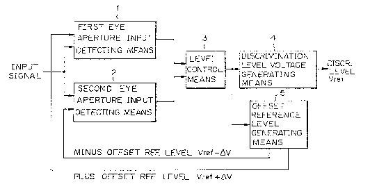
~ igure 2 sllows, as a basic construction of the
present invention, a construction of a circuit for
generating a discrimination level voltage Yre~ whicil is
used as a referencs voltage to discriminate between two
logic levels IIIGII and LO~ adjacent to each other in
input signals which can be generally in a state
corresponding to one of a plurality of di~ferent logic
; levels.
In ~ig. 2, reference numeral 1 denotes a first eye
aperture input detecting means, 2 denotes a second eye
aperture input detecting means, 3 denotes a level
control means, 4 denotes a discrimination level voltage
generating means, and 5 denotes an offset reference
level generating means.
The discrimination level voltage generating means
4 generates the discrimination level voltage Vref .
The offset reference level generating means 5
generates a plus offset reference level Vre, + ~ V
which is higher than the discrimination level Vre~ by a
predetermined offset value ~ V, and a minus offset ;
reference level Vre~ - ~Y which is l~wer than the
discrimination level Vre~ by the predetermined of~set
-10~ 13~6~7'~9~
value ~ V.
The first eye aperture input detectlng means 1
detects that a voltage of the input signal ;s between
: the discrimination level Vrer and tlle ylus offset
refsrence level Vre~ + ~V.
The second eye aperture input detecting means 2
detects that a voltage of the input signal is between
the discrimination level Vre~ and the minus offset
reference level Yr e t ~ ~ V .
The level control means 3 co~trols output voltages
of the discrimination level voltags generating means 4
and the offset reference level generating means 5, so
that the frequencies of the detections in the first eye
aperture input detecting means 1 and the second eye
aperture input detecting means 2 are the same.
According to the present invention, if the
distribution 100 of voltages of input signals
representing the IIIGII level has been shifted down from
the IllGI~ level, as shown in ~ig. 3A, the frequency of
~` ~ the detections in the first eye aperture input detecting
means l is shown as an area of the region l'h~, and the
frequency of the detections in the second eye aperture
input detectlng means 2 is shown as an area of the
region "B in ~ig. 3~. Due to the above down shift of
~ the ~istribution 100, the position o~ the discrimination
level Vr~r relative to the positions of the two
distributions 100 and 110 is deviated toward the
distributions 100, and therefore, the area ~A becomes
larger than the area "~", i.e., the frequency Or the
detections in the first eye aperture input detecting
means 1 becomes larger than the fre~uency of the
detections in the second eye aperture input detecting
~eans 2.
Corresponding to the above difference between the
frequencies of the detections in the first eye aperture
input detecting means 1 and the second eye aperture
: input detecting means 2, the level control means 3
30 ~7~
controls volta~es output by the ~iscrimination levsl
voltage generating means 4 and the offset reference
level generating means 51 so that tlle frequencies of the
detections in the first eye aperture input detecting
means 1 and the second eye aperture input detecting
means 2 are the same, i.e., in this case, the level
control means 3 controls the discrimination level
voltage generating means 4 and the offset reference
level generating means 5 to down shift the output
voltages Yre~ ~ Vrer + ~Vt Vre~ - A V to Vr~r~ ~ Vr~
,' + ~ V' , Vre,' - ~ V' as sllown in ~ig. 3B,
corresponding to the above difference of tbe
frequencies, i.e., corresponding to the voltage shift of
the distribution 100, so that the area ~" becomes
equal to the area ~B~ as shown in Pig. 3B, i.e., the
frequency of the detections in the first eye aperture
input detecting means 1 becomes equal to the frequency
of the detections in the second eye aperture input
detecting means 2.
If the distribution llU of voltages of input
signals representing the LOW level has been shifted up
from the LOW level, as shown in Fig. 4A, the position of
the discrimination level Yre~ relative to the
positions of the two distributions 100 and 110 is
deviated toward the distributions tlO, and therefore,
the area ~ becomes larger than the area UA", i.e., the
frequency of the detections in the second ~ye aperture
input detecting means 2 becomes larger than the
frequency of the detections in the first eye aperture
input detecting means 1.
Corresponding to the above difference between the
fre~uencies of the detections in the first eye aperture
input detecting means 1 and the second eye aperture
input detscting means 2, tlle level control means 3
controls the discri~ination level voltage generating
means 4 and the offset reference level generating means
5, to up shift the output voltages Vre~, Yr~r +~V~ V
' ' .i ~, ~; , '
.
-12- ~L3q)~t77l~
r~ V to ~Ire r , Vre ~ ~ ~ V ~ Vre t - ~ V
' as shown in Pig. 4L, corresponding to the above
difference of the frequencies, i.e., corresponding to
the voltage sllift of the distribution 110, so that the
area "An becomes equal to the area "B~ as shown in ~ig.
4B, i.e., the frequency of the detections in the first
eye aperture input detecting means l becomes equal to
the frequency of tlle detections in the second eye
; aperture input detecting means 2.
1~ ns mentioned above, according to the present
invention, the deviation of the position of tbe
discrimination level VreS relativs to the positions of
the two distributions 100 and 110 is detected as the
difference between the frequency at which the levels of
the input signals lie in the upper half of the vicinity
of the discriminatlon level and tlle frequency that the
levels of the input signals lie in the lower llalf of
the vicinity of the discrimination level, and the
discrimination level is controlled so that tlle above
difference becomes zero, i.e., the deviation of tlle
position of the discrimination level Vre~ relative to
the positions of the two distributions 100 and 110 is
made zero.
`~ Therefore, generally, an error rate hhen
discriminating between different Isvflls of input
signals can be reduced regardless of tll8 tylle of
fluctuation of t1le levels of the input signals, witllout
a manual adiustment, and in particular, in the case of
two-state signals, and whsn the frequency of occurrence
of input signals representing the IIIGII level and the
frequency of occurrence of input signals representing
the LOW level can be deemed to be almost the same, the
error rate can be further reduced.
., ........ . ~ ,~ . . .
--13 ~ 3~ 6~
~igure 5 shows the construction of the first and
second embodiments of the present invention.
In ~ig. 5, reference number 10 denotss a first
sub-discriminating circuitt 11 denotes a main
; 5 discrimination circuit, 12 denotes a second 9ub-
discrimination circuit, 13 denotes a first discord
detection circuit, 14 denotes a second discord detec~ion
circuit, 15 denotes a control signal generating circuit,
and 16 denotes a reference level generating circuit.
The main discrimination circuit 11 discriminates
betwee~ different logic levels of digital input signals.
and component parts other than the main discrimination
circuit 11 in ~ig. 5 constitute the first and second
embodiments of the present invention.
The reference level generating circuit 16
generates a discrimination level voltage Vrat~ a plus
offset reference level Vre,+ ~ V, and a minus offset
reference level Vret- ~Y. .
The diserimination level voltage Vr~r is supplied
to the discrimination circuit, and is used as a
reference voltage to discriminate between diffsrent
Ievels of input signals
The plus offset reference level Vr~ V is
higher than the discrimination level Vrr~ by a
predetermined offset value ~ V, and the minus offset
reference level Vrer- ~ V i9 lower tban the
discrimination level Vr.a, by the predetermined offset
value av.
Namely, the reference level ~enerating circuit 16
corresponds to the aforementioned discrimination level
voltage generating means 4 and the afvrementioned
offset reference level generating ~eans 5 in ~ig. 2.
The first sub-discrimination circuit 10 compares
the dieital input signal with the plus offset reference
level Yrer+ ~ V, and outputs a high level signal or a
low level signal respectively, according to whether a
level of the input digtal signal is higher or lower than
30~
tlle ~)lus offset reference level Vr~ V, a~d lll0
second sub-d;scrimination circuit 12 compares the
digital input signal Vr~ wit~l the minus offset
reference level V r e t - ~ V ~ and outputs a high level
signal or a low level signal respect;vely, according to
whether a level of tile input signal is higher or lower
than the min~s offset reference level Vr~ Y.
- In the first embodiment of the present invention,
the first discord detection circuit 13 detects a discord
between the output of the first sub-discri~inat;on
circuit 10 and the digital input signal (whicll is the
object of level discrimination in the discrimination
circuit 11), and similarly, the second discord
detection circuit 14 detects a discord between the
output of the second sub-discrimination circuit 12 and
the digital input signal.
In the second embodiment of the present invention,
the first discord detection circuit 13 detects a
discord between the output of the first sub-
discrimination circuit 10 and the discrimination result
obtained by comparing the digital input signal with the
discrimination level ~tbe output of the main
discrimination circuit 11), and the second discord
~; detection circuit 14 detects a discord bet~een the
output of the second sub-discrimination circuit 12 and
the discriMination rssult obtained by comp~ring the
digital inPut signal with ths discrimination level (tbe
output of tbe main discrimination circuit 11).
The control signal generating circuit 15 realizes
the level control means 3 in Pig. 2, and the control
signal generating circuit 15 functions as a dlfference
obtaining means, and obtains a difference between the
frequencies of the detections in the first and second
eye aperture input detscting means 1 and 2, i.e., the
frequencies of the detections in the first and second
discord detection circuits 13 and 14, and controls the
output of the reference level generating means 16, i.e.,
'
:
-15- 1 3~
tlle discrimination level voltage Vre7, the plus offsel
reference level Vre~ ~V~ and the minus oSfset.
reference level Vr~ V, so that the frequencies of
the detections in the first and second discord detection
circuits 13 and 14, are the same. Namely, the control
signal generating circuit 15 causes the reference level
gensrating circuit 16 to raise or lower tlle output
voltage Vreg (and accordingly, the plus offset
reference level Vre~ and the minus offset
reference level Vre~- ~ V) according to tlle difference
between the frequency of the detections in the first
discord detection circuit 13 and the frequency of tlle
detections in tlle second discord detection circuit 1~.
The first sub-discrimination circuit 10 and the
first discord detection circuit 13 realize the first eye
aperture input detecting means 1 in ~ig. 2, and the
second sub-discrimination circuit 12 and the second
discord detection circuit 14 realize the second eye
aperture input detecting means 2 in ~ig. 2.
~ igure 6 shows the construction of an example of
the main discrimination circuit 11, or tlle first or
second sub-discrimination circuit 1~ or 12.
In ~ig. 6, reference numeral 51 denotes a
comparator, and 51 denotes a D-type fllp-flop circuit.
As a reference input of tlle comparator 51. the
atorementioned discrimination level voltage Vro, is
input to the main discrimination circuit 11, the
aforementioned plus offset reference level Vr~5~ ~ V
i9 input to the first sub-discrimination circuit 10. and
the aforementioned minus offset reference level VreS~
V is input to the second sub-discrimination circuit 12.
~ s an object of the comparison with the reference
input, the aforementioned digital input signal is input
in all of the cases to the mai n discrimination circuit
11, the first sub-discrimination circuit 10, and the
second sub-discriminatioll circuit 12.
In each of the above cases, the output of the
,
-16- ~L3~67~
comparator 51 is held in the D-type flip-flop circuit 52
in the timing of each bit input of tlle digital Input
; signal.
Each of the first and second discord detection
circuits 13 and 14 can be realized by an exclusive OR
circurt 53 as sllown in ~igure 7.
Figure 8 shows an input-output relationsllip and a
timing of the exclusive OR circuit 53 in i7ig. 7; nS
sllown in ~ig. 8, when a discord appears between the
output of the first or second sub-discri~ination circuit
10 or 12 and the output of the main discrimination
circuit 11 in tlle second embodiment (or when a discord
appears between the output of the first or second sub-
discrimination circuit 10 or 12 and the aforementioned
digital input signal in the first embodiment), the first
or second discord detection circuit 13 or 14 outputs an
effective pulse signal.
~ igures 9, 10, and 11 eacll show a cuncrete exam~)le
of the aforementioned difference obtaining means.
~ 20 In Pig. 9, reference numerals 60 and 61 denole
- first and second counters, and 62 denotes a subtractor.
The counter 60 counts the effective pulse signals
from the first discord detection circuit 13 as mentione(l
above, and similarly, the counter 61 counts the
effective pulse signals from the second discord
detection circuit 1~. The difference between the count
outputs of tlle counters 60 and 61 is obtained in tlle
subtractor 62 at a predetermined interval, for example,
every one second. Tlle counters 60 and 61 are reset
before at least one of same overflows.
In Pig. 10, the construction simîlar to Fig. 9 is
realized by an up-down counter 63 having a count up
input terminal and a count-down input terminal; tlle
count of which counter is incremented at the timing of
an input of a new effective pulse from the count-up
input and is decremented at the timing of an input of a
new e~fective pulse from the count-down input.
--17 ~ 3 ~ 4
Therefore, when the output of the first discord
detection circuit 13 is applied to the count-up input,
; and the output of the second discord ~etection circuit
1~ is applied to the count-down input, the up-down
counter G3 outputs the difference between the outputs
of the first and second discord detection circuits 13
and 14. In the construction of the ~ig. 10. a reset
operation of tlle counter 63 is not necessary.
In ~ig. 11, reference numerals G4 and 65 denote
first and second counters, 66 denotes a subtractor, 67
denotes an adder, and 68 denotes a U-type flip-flo~
circuit.
Similar to the construction of the ~ig. 9, the
counter 64 counts the effective pulse signals from the
first discord detection circuit 13 as mentioned above,
and the counter 65 counts the effective pulse signals
from the second discord detection circuil l~. The
difference between the count outputs Or the counters
and 65 is obtained in the subtractor 66 at a
2~ predetermined interval, for example, every one second,
and then tlle output of the subtractor 66 is applied to
tbe adder 67 and is added to the output of the U-type
flip-flop circuit 63 in the adder 67. The D-type flip-
flop circuit 68 holds the output of the adder 67 at each
predetermined time, i.e.. tlle output of the D-type
flip-flop circuit 68 i9 renewed by the output of lbe
adder 67 at each predetermined time.
The counters 64 and 65 also must be reset before
one of same overflows, but in this construction, tlle
pasl data of the difference of the frequencies Or the
detections in the first and second discord detection
circuits 13 and 14 is stored in tlle D-type flip-rlo~
circuit 68, and is reflected in tlle output of the
constructlon of ~ig. 11 through tlle adding operation in
the adder 67.
~lthougll tlle up-down counters available on tlle
market tend to operate rather 510wly, compared Witll the
3~ 7'~4
simple countsrs, a function similar to the construction
of ~ig. 10 can be realized by the construction of Pi~.
11, with a faster operation speed.
~igure 1~ also shows anotller concrete example of
; 5 the aforementioned dlfference obtaining means.
In ~ig. 12, reference numerals 71 and 72 denote
first and second accumulation means, for exa~ple,
capacitors, and 73 denotes a differential amplifier.
Each of the outputs of tbe ~irst and second
discord detection circuits 13 and 14 is applied to the
corresponding one of two input terminals INPUT1 and
INPUT2. and the charges generated by the aforementioned
effective (high voltage) pulses are accumulated in the
corresponding one of the capacitors 71 and 72.
~ccordingly, the voltage between the own terminals of
each capacitor is almost proportional to the number of
effective pu Ises input from the corresponding input
terminal, i.e., tlle frequency of the detections in the
corresponding discord detection circuit,
The analog voltage in proportion to the difference
between the voltages accumulated at the capacitors 71
; and 72 is obtained by the differential amplifier 73.
Each of the outputs obtained in the constructions
of ~igs. 9, 10, 11, and 12 corresponds to the control
output from the level control means 3 in ~ig. 2.
~i~ure 13 shows the constructlon of an example ol
the reference level generating means 16 in ~ig, 5.
In Fig. 13, reference numeral 75 denotes a linear
amplifier, '16 denotes a transistor, 77 denot0s a diode,
3~ and 78, 79, 80, and 81 denote resistors.
The ampl;fier 75 is constructed by a differential
amplifisr, and a reference voltage is applied to one of
the two input terminals of the amplifier 75 and the
aforementioned control output of the level control means
3, i.e., the OUtp(lt of the control signal generating
means 15 is applied to the other input of the
differential amplifier 75, and thus, the control output
..
. :
,
. . :
-19- ~L3~6~74
i9 amPliried in the amplifier 75, and then applied to
the base terminal of the transistor 76.
The colIector terminal of the transistor 76 is
connected to a high voltage source, and the emitter
terminal o~ the transistor 76 is connected to one
`; terminal of a series connection of the diode 77 and the
resistors 78, 79, 80, and 81, where She other terminal
of the series connection is connected to the earth level.
By the above construction, the current flowing in
the transistor 76, i.e., the current flows in each of
the resistors 78, 79, 80, and 819 is controlled by the
base voltage of the transistor 76. i.e., the control
output of the level control means 3.
ns the input Or the construction of ~ig. 13 is an
~5 analog signal, the analog output of the construction of
; ~ig. 12 can be applied to the input terminal of the
construction of ~ig. 13, but each of the outputs in the
construction of Fig. 9. 10, and 11, as digital data,
must be connverted to the analog voltage before applied
to the construction of ~ig. 13, by, for exa~ple, a
digital-to-analog converter as shown in ~igure 14.
; In particular, if the posslbility of occurrence of
an error is very low, i.e., the frequency of the
detections in the flrst or second discor~ detection
means 13 or 14 is very low, for example, If the
possibility i9 about 1 X 10-U, it is imPossible to detect
the difference of the frequencies b~ the construction
of ~ig. 12, and therefore, in such a case, the
constructions using counters as shown in ~igs. 9, 10,
and 11, are effective.
.~
.