Note : Les descriptions sont présentées dans la langue officielle dans laquelle elles ont été soumises.
1 3n~57
IMPROVED PLASTIC ORIFICE PLATE FOR AN
INK JET PRINTHEAD AND METHOD OF MANUFACTURE
Technical Field
This invention relates generally to the
manufacture of orifice plates for ink jet pens and more
particularly to the manufacture of a plastic orifice
plate for a thermal ink jet printhead. This orifice
plate may, if desired, be made transparent in order to
view fluid dynamics within the pens.
Backqround Art_and Related Applications
In the manufacture of disposable pens for thermal
ink jet printing systems, it has been one practice to
employ metal electroplating processes to form the outer
ink ejection orifice plate of the pen to a desired
contoured geometry. This orifice plate is also
sometimes referred to as a nozzle plate, and will
typically be adhesively secured to and precisely aligned
with an underlying thin film resistor (TFR) substrate.
In this structure, a plurality of resistive heater
elements will normally be aligned with an associated
plurality o~ ink reservoirs from which ink is ejected
through orifice openings in the covering orifice plate
during an ink jet printing operation. This type of
thin film resistor printhead structure is described, for
example, in the Hewlett-Packard Journal, Vol. 36, No. 5,
May 1985.
In addition to the above HP Journal disclosure,
other types of nickel orifice plates and related
Case 187110
1 3 ,957
electroforming processes are described in U.S. Patent
4,694,308 issued to C.S. Chan et al entitled "Barrier
Layer and Orifice Plate for Thermal Ink Jet Printhead
Assembly", and in U.S. Patent No. 4,716,423 issued to
C.S. Chan et al entitled "Barrier Layer and Orifice Plate
for Thermal Ink Jet Print Head Assembly and Method of
Manufacture". Both of these patents are assigned to the
present assignee. In addition to the above disclosures,
a related electroforming process for manufacturing a
compound bore nickel orifice plate for an ink jet
printhead is disclosed and claimed in U.S. Patent No.
4,675,083 issued to James G. Bearss et al on June 23,
1987, also assigned to the present assignee.
The metal orifice plates disclosed in the above
identified references have proven highly acceptable in
terms of improving ink ejection efficiency and
performance and in reducing ink cavitation wear and ink
corrosion, thus increasing the printhead lifetime.
However, these metal orifice plates are opaque and thus
do not enable one to actually view the fluid dynamics
which occur beneath the orifice plate and above the
associated thin film resistor substrate during an ink jet
printhead testing and evaluation operation.
1 3n~o57
Disclosure of Invention
Accordingly, it is an object of an aspect of
the present invention to provide a new and improved
plastic orifice plate and process for fabricating same
wherein preferred orifice geometries and spacings of
the types disclosed in the above Chan et al and Bearss
et al inventions are preserved.
An object of an aspect of the invention is to
provide a new and improved transparent plastic orifice
plate and process for fabricating same wherein one may
view the actual fluid dynamics through the orifice plate
and occurring above the printhead substrate during
printhead testing and evaluation.
An object of an aspect of the invention is to
provide a plastic orifice plate and related process of
the type described in which durable and economical
orifice plates may be reliably reproduced at high
yields.
An object of an aspect of the invention is to
provide a new and improved plastic orifice plate which
may or may not be transparent and which is non-
corrosive.
An object of an aspect of the invention is to
provide a new and improved plastic orifice plate of the
type described in which integral barrier layers may be
~ 3''~q57
formed with an outer orifice plate for subsequent
attachment to a thin film resistor or equivalent energy
generating substrate. Thus the requirement for
providing intermediate polymer barrier layers may be
eliminated and the overall printhead fabrication cost is
reduced.
The above objects and attendant advantages and
features of this invention are achieved by the provision
of a manufacturing process which includes electroforming
a metal die so as to have raised sections of a preferred
contoured surface geometry which replicates the desired
internal surface geometry of a plastic orifice plate. A
plastic preform of a preselected thickness is then
brought into physical contact with the metal die in such
a manner that the raised sections of the die are punched
through the plastic preform to thereby form a plurality
of closely spaced and contoured orifice openings
therein. When it is desired to view fluid dynamics and
the like within the underlying printhead substrate, then
one obviously would use a clear transparent plastic
preform in the above manufacturing process.
Other aspects of this invention are as
follows:
A process for forming an orifice plate for an
ink jet printhead which comprises:
a. providing a metal die having raised contoured
convergent mesa-shaped sections therein with predefined
1 3 r` Q` ~ 57
5A
center-to-center spacings which define desired
corresponding center-to-center spacings of orifice
openings in an ink jet orifice plate,
b. bringing said die into physical contact with a
preform of a preselected material and thickness so that
said raised sections of said die punch through said
preform and thereby form contoured convergent orifice
geometries therein, and
c. removing said preform from said die and
exposing said preform to a plasma reaction to remove
flashing from the punched-formed orifice openings
therein.
A process for forming convergent orifii in a
thin layer to form an orifice plate which comprises the
15 steps of:
a. electrodepositing a first metal layer on a
substrate having a plurality of closely spaced islands
thereon to leave openings in said first metal layer
aligned with said islands,
b. forming a second metal layer on said first
metal layer and having smoothly curved convergently
contoured mesas therein extending into openings in said
first metal layer to form a metal die,
c. separating said first and second metal layers,
and
d. using said second metal layer defining said
A
1 3 i 3 q, 7
5B
metal die to stamp out openings in a thin layer of a
selected material to form convergent orifii therein.
A process for forming a die useful in creating
closely spaced convergent openings in thin layers of
selected materials which comprises the steps of:
a. providing a substrate of a chosen material,
b. forming islands of material adherent to the
upper surface of said substrate,
c. depositing a first metal layer on top of said
substrate and having openings therein aligned with said
islands,
d. depositing a second metal layer atop said
first metal layer and having smoothly curved convergent
mesas extending into said openings of said first metal
layer, and
e. separating said first and second metal layers
to thereby leave said second metal layer in the shape of
a metal die having a plurality of convergently contoured
mesa regions extending from one surface thereof.
A process for forming a die useful for
stamping convergently contoured openings in thin layers
of certain chosen materials, which comprises the steps
of:
a. forming a first layer of a selected material
on a substrate having islands thereon of a controlled
lateral extent and spacing, so that openings are formed
in said first layer which are aligned with said islands,
1 3 ~ , 7
5C
b. forming a second layer of a selected material
on top of said first layer, so that smoothly curved
convergently contoured mesas are formed as part of said
second layer and extend into said openings in said first
layer, and
c. separating said first and second layers so as
to leave said second layer useful as a stamp-out die.
A metal die useful in the manufacture of
orifice plates and comprising a metal substrate having a
plurality of smoothly and convergently contoured mesa
regions extending therefrom and spaced apart by a
predefined distance.
The above summary of this invention will
become better understood from the following description
of the accompanying drawings.
Brief Description of the Drawinas
Figures lA through lH illustrate in a sequence
of isometric views the various process steps which are
carried out in accordance with a preferred embodiment of
this invention.
Figures 2A through 2H are cross section views
corresponding to Figures lA-lH and are taken along lines
1 3n'!957
2-2 of Figure lA by way of example for one set of
figures lA and 2A.
Detailed Description of the Drawinqs
Referring now to the corresponding isometric and
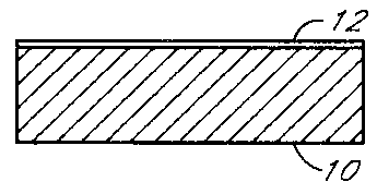
cross section views in Figures 1 and 2, respectively, a
stainless steel substrate 10 is coated with a thin layer
of photoresist 12 in a well known manner and in
accordance with teachings of the above identified Chan
et al patent or application. The photoresist 12 is then
treated with conventional photolithographic masking, W
exposure and development processes to form a photoresist
mask 14 which is cylindrical in shape as indicated in
Figures lA and 2B.
The masked structure of Figures lB and 2B is then
transferred to a nickel electroforming station wherein a
first, surface layer 16 of nickel is formed in the
geometry shown in Figures 3A and 3B, including a
convergent orifice opening 18 which forms concentrically
with the mask 14 as described in further detail in the
above identified Chan et al inventions. The use of the
circular mask 14 in the manner shown enables the nickel
to plate up over the outer edge of the mask and in so
doing form the convergent orifice opening 18. However,
it will be understood that the single opening 18 is
merely representative of a plurality of openings which
ultimately correspond to a plurality of orifice openings
in the plastic orifice plate manufactured in accordance
Case 187110
1 3""957
with the "stamp-out" or "punch-through" process
described in more detail below.
The structure in Figures lC and 2C is then placed
in a chemical bath to remove the photoresist mask 14 and
then transferred to an oven and heated to about 150C
for approximately two hours to form a thin nickel oxide
layer 20 thereon as shown in Figures lD and 2D. The
latter structure is then removed from the oven and taken
again to the nickel electroforming station where another
layer 22 of nickel is electroformed to a thickness of
approximately 3 mils. This second nickel layer 22 is
shown in Figures lE and 2E, and the purpose of the
nickel oxide layer 20 is to serve as a separation layer
between the first and second nickel platings 16 and 22.
The second nickel layer or plating 22 is the die for the
subsequent plastic orifice plate-forming step to be
described. The nickel die 22 may be easily stripped
away from the underlying nickel oxide layer 20 by the
use of an adhesive tape applied to both the nickel die
22 and the stainless steel substrate 10 to thereby leave
the resultant die structure in the geometry indicated in
Figures lF and 2F.
The nickel die 22 in Figures lF and 2F is then
taken to a heat staker station as indicated in Figures
lG and 2G where it is first placed upon a thin clear
transparent plastic disc 24 of approximately 2.0 mils in
thickness and then inserted between two pieces of glass
26 and 28. Here heat of approximately 200C and
Case 187110
1 3 !~ r 7
pressure of approximately 120 pounds per sguare inch are
applied to the die 22 and transparent plastic preform 24
so as to cause the contoured mesa section 30 of the die
22 to punch through the thin plastic preform 24 and
thereby form the convergently contoured orifice opening
32 in the plastic preform structure shown in Figures lH
and 2H.
The thus formed transparent orifice plate
structure 34 shown in Figures lH and 2H is then placed
in a plasma reactor wherein the plastic surface
flashing on the plastic orifice plate is removed under
the following reactor conditions:
gases = CF4 and 2
power = 200 watts,
pressure = 0.7 Torr
and
time = 2 minutes.
This latter procedure will remove approximately 0.1 mil
of plastic flashing material from the surface of the
plastic orifice plate 34, thereby leaving a clean
circular edge 36 as the output edge of the convergent
orifice opening 32.
Although the clear plastic preform 24 may be
easily obtained through commercial channels, this
transparent substrate material was made as follows
during the actual reduction to practice of this
invention and therefore represents a part of the
presently known best mode for carrying out the
Case 187110
1 3!~,q57
invention. First, a polycarbonate disc was provided and
cut into pellets of approximately 1/8 inch cube. Then
the pellets were sandwiched between two glass plates and
heated to approximately 200C and under an applied
pressure of 50 psi for about 2 minutes. This initial
process yielded polycarbonate discs of 12 mils in
thickness and of about 0.5 inches in diameter.
Next, the above discs were again placed between
two glass plates (not shown) which were supported by 2
mil metal substrates (not shown) to control the ultimate
preform thickness. Then heat of approximately 200C and
pressure of approximately 100 psi were applied to these
discs for about 2 minutes to thereby yield the final
plastic preforms 24 of about 2.0 mils in thickness.
It will of course be understood that the above
description of the formation of a single orifice 32 is
only one of many orifices (not shown) which will be
simultaneously formed in the transparent orifice plate
in accordance with the number, geometry and spacing of a
plurality of mesa-like sections 30 on the die 22. Thus,
the present invention obviously extends to the
formation of either one or a plurality of orifices 32
arranged in any desired geometry.
Additionally, the present invention is not
limited to the formation of only single step convergent
nozzles and may instead employ either the compound bore
geometry approach disclosed in the above Bearss et al
U.S. Patent 4675083 or alternatively the double layer
Case 187110
1 3 ~or~7
nickel geometry disclosed in the above identified Chan et
al inventions in forming the die 22, or still
alternatively the serrated bore orifice geometry
disclosed in Canadian patent application serial no.
572,045 of C.S. Chan et al. When using the double layer
nickel process to make the nickel die 22, the mesa
section 30 would become a stepped double layer mesa
section which could then be used to form an integral
multi-layer plastic barrier layer and plastic orifice
plate structure similar to the metal barrier layer and
metal orifice plate structure described in the first two
above identified Chan et al inventions. In this latter
alternative embodiment, the creation of the integral
plastic barrier layer and orifice plate structure would
make possible the elimination of well known polymer
barrier layers of the prior art, such as barrier
materials known in the art as RISTON and VACREL which are
tradenames of the DuPont Company.
The following table of dimensions is given by way of
example only.
Table
. Layer Thickness Diameter of Center-to-
Orifice Center Orifice
Spacing
16 2 mil 2.0 mil 6-7 mil
1000 A N/A 6-7 mil
22 2 mil 2.0 mil 6-7 mil
34 2 mil 2.0 mil 6-7 mil
B
1 ~ ~, rl 7
11
Although the present invention is primarily
directed to the processing of plastic transparent non-
metallic orifice plate preforms, it is not so limited
and may be used in processing any preform material which
lends itself to the "punch through" die stamping
operation disclosed and claimed herein.
Case 187110