Note : Les descriptions sont présentées dans la langue officielle dans laquelle elles ont été soumises.
~31~9~68
`" -1- RCA 84,274
CHROMA OVERLOAD DETECTOR USING
A DIFFERENTIAL AMPLIFIER
FIELD OF THE INVENTION
This invention relates generally to the field of
television color signal processing circuitry and
specifically to the field of chroma overload detector
circuitry.
BACKGROUND OF THE INVE~TION
The term "kine" as used herein means color
television picture tube.
In order to prevent objectionable variations in
the level of the chrominance signals displayed on the
screen of a color television receiver, it is well known to
employ an automatic chrominance control (ACC) circuit. ACC
circuits typically operate in a closed loop configuration
and vary the gain of a first chrominance amplifiex in
response to the amplitude of the color burs~ component of
the received television signal.
The ACC circuitry will not function properly if
the ratio of the burst amplitude to chrominance in the
received televis.ion signal is incorrect. This incorrect
ratio may be due to problems originating at the
broadcaster's transmitter, or because of reflections of the
signal along the signal path between the transmitter and
television receiver. Such an incorrect ratio may cause an
overload condition to occur. The response of the ACC
circuitry is typically not fast enough to prevent an
overload condition from being displayed on the screen. The
overload may manifest itself as one or more television
lines having an objectionably saturated color level which
may resemble a smearing effect. In order to solve this
problem, chroma overload circuitry is employed to detect an
overload condition and control the gain of a second
chrominance amplifier accordingly.
An example of chroma circuitry employing a chroma
overload detector is known from U.S. Patent 4,054,905
(Harwood, et al.). While this circuitry performs well, it
~';S~
.
.
13~91~8
-2- RCA 84,274
has certain features which may make it not optimally suited
for integration in modern integrated circuits which tend to
be more densely packed than those of a decade ago.
For example, the circuitry of Harwood, et al.
requires a æener diode and a relatively large value
resistor (approximately 40K ohms). Zener diodes are not
readily available in the technology used in the design and
manufacturing of today's densely packed integrated
circuits, and because large value resistors require too
much area, their use is to be avoided, if possible.
SUMMARY OF THE INVENTION
It is herein recognized that the above-noted
problems inherent in prior chroma overload detectors can be
eliminated by using a differential amplifier as a
comparator in a chroma overload detector circuit.
Speciically, the integrability of the circuit is enhanced
in that a zener diode and large valued resistor are no
longer necessary. It is additionally recognized that
temperature variations are more easily compensated when a
differential amplifier chroma overload detector is used
because the other chroma proces~ing stages utilize
similar differential amplifier stages as well.
BRIEF DESCRIPTION OF THE DRAWING
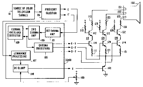
FIGURh' 1 shows, partly in block diagram form and
partly in schematic diagram form, the portions o a
television receiver which are relevant to the subject
invention.
FIGURE 2 shows in schematic diagram form an
embodiment of the invention suitable for use in the
television receiver of FIGURE 1.
DETAILED DESCRIPTION OF THE DRAWING
The portion~ of a television r~ceiver relevant to
the inven~ion are shown in FIGURE l. A source of color
television signals 10 supplies signal to a frequency
selection unit 20 which separates chrominance signals C and
unprocessed luminance signals Y' and applies them to a
~ multifunction high density integrated circuit IC100. IC100
-~ may also contain sound processing and deflection circuitry
~3~
-3- RCA 84,274
(not shown) which are not relevant per se to this
invention.
Chrominance signals C are applied via a first
chrominance amplifier (lst chroma amp.) lO1 and a second
chrominance amplifier (2nd chroma amp.) 103 to a chroma
processing unit 105 which derives R-Y, G-Y, and B-Y signals
therefrom. Unprocessed luminance signals Y' are applied to
luminance processing unit 107, the output of which is
clamped to the proper level by d.c. clamp 108, and applied
to the base of luminance bufer amplifier 140. R-Y, G-Y
and B-Y signals are applied to the input of kine driver
amplifiers 110, 120 and 130 respectively.
Each of these kine drive amplifiers is arranged
in a cascode configuration as is well known. Kine driver
amplifiers llO, 120 and 130 comprise cascode-connected
transistors 112 and 114, 122 and 124, and 132 and 134
respectively. Luminance signals are applied to the
emitters of transistors 114, 124 and 134 via coupling
resistors 111, 121 and 131. AmpliEied video signals are
applied to the individual cathodes 151, 153, 155 of kine
150 via load resistors 113, 123 and 133 respectively. Base
bias or transistors llZ, 122 and 132 is provided by
resistors 115, 125 and 135 respectively.
D.C. clamp 108 may be a keyed clamp of the type
~unown from IJ.S. Patent 4,197,557 (Tuma et al.)
Specifically, it has an input terminal to which the wiper of
a brightness control 160 is coupled. Manual operation of
the brightness control affects the d.c. level of the
luminance signal and thus the brightness of the picture
displayed on kine 150 .
The amplified chrominance signal produced by the
second chrominance amplifier 103 is also applied to a
chroma overload detector 109, the function of which will be
explained in detail below.
The first chrominance amplifier 101 is gain
controlled by automatic color control (ACC) circuitry, not
shown. ACC circuitry is well known in the art from, for
example, U.S. Patent 3,740,462 (~arwood). Briefly, ACC
131~9~i8
-4- RCA 84,274
circuitry is responsive to the color burst component of a
color television signal and acts to maintain the amplitude
of the burst information at the output of the first
chrominance amplifier at a constant level. If each
television broadcaster adheres to system standards
concerning the relative levels of picture-chroma and burst
information in its signals, the chroma signals will be
maintained at the same color saturation level despite the
viewer switching from one channel to another.
Chroma overload detector 109 responds to the
amplitude of the chrominance signals at the output of the
second chrominance amplifier 103, when the signals exceed a
predetermined threshold level, by generating a gain control
signal and applying it to the second chrominance amplifier
103 to reduce its gain.
FIGURE 2 shows in detail the chroma overload
circuitry of element 109 of FIGURE 1. l`he chroma overload
detector comprises a differential amplifier including
transistors 244 and 246 which have their respective
emitters connected together and returned to ground via a
current source transistor 248 and a resistor 249. The
collectors of transistors 244 and 246 are coupled via load
resistors 245 and 247, respectively, to a voltage source
V~.
The chrominance si~nal input circuitry of the
diferential amplifier is provided by buffer amplifier
transistor 214, and its base bias resistor 212. The
emitter of transistor 214 is coupled to the collector of
diode-connected transistor 240 which is in turn connected
in series with another diode-connected transistor 242.
Diode-connected transistor 242 is returned to ground via
resistor 243. Two series-connected resistors 201 and 202
are connected in parallel with the series combination of
diode connected transistors 240 and 242.
The predetermined threshold level mentioned above
is established by the circuitry coupled to the base of
transistor 246. It should be noted that the circuitry of
one-half of the differential amplifier essentially mirrors
.
.. . . .
~ 3(~i91E;13
-5- RCA 84,274
that on the other half with one important e~ception to be
discussed below. Transistor 254 has an associated bias
resistor 255 and has its emitter coupled to the collector
of diode-connected transistor 250 which is in turn coupled
in series with another diode-connected transistor 252.
Diode-connected transistor 252 is returned to ground via
resistor 253. Two series-connected resistors 203 and 204
are connec-ted in parallel with the series combination of
diode-connected transistors 250 and 252.
The important exception to the symmetry between
the two sides of the differential amplifier is that the
base of transistor 244 is connected to the top of the
series pair of resistors 201 and 202, while the base ~f
transistor 246 is connected to the connection point between
resistors 203 and 204.
In order to properly balance the amplifier, the
values of resistors 201 and 203 should be equal, the values
of resistors 202 and 204 should be equal, and the values of
resistors 243 and 253 should be equal. It is preferable
that resistors 201, ~02, 203, and 204 have values equal to
each other, because in that case they could all use the
same geometry, thereby making the physical layout of the
integrated circuit containing them easier. It is the ratio
of resistors 203 and 204 which sets the predetermined
threshold level by forming a voltage divider across
diode-connected transistors 250 and 252.
In operation, chrominance signals are applied to
the bas~ o~ transistor 214 and replicated on the base of
transistor 244~ Transistor 246 is biased at a lower level
than is transistor 24~, and is normally not conducting.
When the amplitude of the chrominance signals
becomes sufficiently large, the negative excursions of the
signal exceed the level necessary to cut off transistor 244
and allow transistor 246 to conduct. A d.c. output signal
is developed at the collector of transistor 246 which
relates to that portion of the amplitude of the chrominance
signal which exceeds the predetermined threshold level.
The output signal is filtered by elements 232, 234, 236 and
~3~ 8
-6~ RCA 84,274
238 and applied via terminal 260 to the control input of
the second chrominance ampli~ier 103 to reduce its gain.
.
~ ' :
',:;
~ , .
:; :
::
,
,