Note : Les descriptions sont présentées dans la langue officielle dans laquelle elles ont été soumises.
1 30q 1 75
. TITLE OF THE INVENTION
: Reference Signal Producing Circuit for Phase Servo
` Control
BACKGROIJND OF THE INVENTION
Field of the Invention
; The present invention relates generally to reference
`: signal producing circuits, and more particularly to
: improvements in the reference signal producing circuit for
producing a reference signal for phase servo in
synchronization with an external signal such as a
composite synchronizing signal in a motor servo circuit of
a video apparatus such as a video tape recorder
(hereinafter referred to as a VTR ) .
Description of the Background Art
.` ! .
Conventionally, there is provided a mot.or servo
circuit for controlling rotation of a cylinder motor and a
capstan motor in a VTR. In such a motor servo circuit, a
reference signal for controlling phase servo of the motor
is produced based on a composite synchronizing signal
extracted from a video signal. This production of the
: reference signal is in general carried out by employing a
. ; synchronization separator circuit for saparating a
vertical synchronizing slgnal from the composite
synchronizing signal. As an example of this
~:,
.' 25 synchronization separator circuit, a circuit is proposed
. .
~ ............ . .
: , :
. .
;,
1 3~9 1 75
and also disclosed in Japanese Patent Laying-Open No.
61-288579, which includes an up/down counter and thus
controls counting operation of this counter in accordance
with the level of the composite synchronizing signal to
sense the vertical synchronizing signal depending on an
output state of this counter.
Furthermore, this synchronization separator circuit
carries out separation of a horizontal synchronizing
signal for special reproduction in the VTR, which will be
described later.
As ~nother example of the convantional
synchronization separator circuit, a circuit is proposed
which has a compensating funçtion in the case of
incidental one-shot lack of pulses of the vertical
sync~ronizing signal and the horizontal synchronizing
signal within the composite synchronizing signal.
However, no circuit has the compensating function in
the case of successive lack of the plurality of horizontal
synchronizing signal pulses or vertical synchronizing
signal p~lses within the composite synchronizing signal.
Therefore, various problems arise as follows in the case
of the successive lack.
In the case of changing channels durin~ picture
recording in the VTR, for example, supply of the video
signal is generally~lnterrupted to lose the vertical
- 2 -
:
: , .
'' ' '
; ' ' ' ' :
130~75
synchronizing signal and thus synchronization reference
for motor servo. Furthermore, in the case of only
recording a sound in a high fidelity video or the like, or
in the case of being unable to sense the vertical
synchronizing signal because of an extremely weak
broadcasting signal, the vertical synchronizing signal
pulses lack successively, thereby not obtaining the
synchronization reference for phase servo of various types
of motors.
In addition, the following problem occurs in the
special recording in the VTR, in the case that the
horizontal synchronizing signal pulses in the composite
synchronizing signal successively lack from the above
described causes. That is, in the special reproduction in
the VTR, V jitter (very fLne movement of vertical sync) on
a screen is prevented by employing a quasi vertical
s~nchronizing signal in which the plurality of horizontal
synchron.izing signal pulses are inserted immediately
before the vertical synchronizing signal pulse; however,
the V jitter cannot be prevented when the horizontal
synchronizing signal pulses in the composite synchronizing
signal lack successively.
SUMM~RY OF THE INVENTION
It is an object of the present invention to provide a
referenca signal producing circuit h~ving a reference
,
,
l~ql75
signal producing function in the case of successive lack
of vertical synchronizing signal within a composite
synchronizing signal.
It is another object of the present invention to
provide a reference signal producing circuit capable of
; supplying a reference signal having a period equal to that
of the vertical synchronizing siqnal and performing stable
phase servo control, in the case of the successive lack of
the vertical synchronizing signal pulses in the composite
synchronizing signal.
It is a further object of the present invention to
provide a reference signal producing circuit capable of
superior special reproduction even in the case of the
successive lack of horizontal synchronizing signal-pulses
in the composite synchronizing signal.
In short, according to the present invention, a
reference signal producing circuit for producing the
reference signal based on the composite synchronizing
signal externally supplied comprises a separator circuit
for separating the synchronizing signal from the composite
synchronizing signal, a timer circuit being reset by the
reference signal, a compensation signal producing circuit
for comparing an output of the timer circuit with a
variable set value to produce a compensation synchronizing
signal having a variable period, and a reference signal
: .
- ,
: , ~
.
1 309 1 75
output circuit for supplying as the reference signal an
output of the separator circui-t or an output of the
compensation signal producing circuit, the set value of
the compensation signal producing circuit being changed
such that a period of the compensation synchronizing
signal is normally set to a slightly larger value than
that of a synchronizing signal period, while being set to
a value equal to that of the synchronizing signal period
in the case that a predetermined number or more of the
synchronizing signal pulses in the composite synchronizing
signal lack successively.
According to another aspect of the present invention,
the synchronizing signal separated from the composite
synchronizing signal is a vertical synchronizing signal.
Therefore, it is a main advantage of the present
invention that a stable phase servo control can be
performed because the compensation synchronizing signal of
a period equal to that of the original vertical
synchronizing signal can be s~pplied in the case, as in
no-video signal inputtlng, that a predetermined number or
more of the vertical synchronizing signal pu].ses in the
composite synchronizing signal lack successively.
The foregoing and other objects, features, aspects
and advantages of the present invention will become more
apparen~ from the following detailed description of the
-- 5 --
1 ~9 1 75
present invention when taken in conjunction with the
accompanying drawings.
BRIEF DESCRIPTION OF THE DRAWINGS
Fig. 1 is a schematic block diagram illustrating a
motor servo circuit in a VTR employing a reference signal
producing circuit according to the present invention;
Fig. 2 is a block diagram illustrating a reference
signal producing circuit according to one embodiment of
the present invention;
Fig. 3 is a timing chart for illustrating an
operation of a horizontal processing bloc~ in the
reference signal producing circuit shown in Fig. 2;
Figs. 4-6 are timing charts for illustrating an
operation of a vertical processing block in the reference
signal producing circuit shown in Fig. 2;
Fig. 7 is a flow chart for illustrating a
compensating operation of the embodiment shown in Fig. 2;
Fig. 8 is a timing chart for illustrating the
compensating operation of the embodiment shown in Fig. 2;
Figs. 9 and 10 are timing charts for illustrating an
even/odd number field deciding operation in the embodiment
shown in Fig. 2;
Fig. 11 i~ a block diagram illustrating a reference
signal producing circuit according to another embodiment
of the present inv~ntion; and
-- 6 --
,, ~
.
1309175
Fig. 12 is a timing chart for illustrating the
operation of the horizontal processing block in the
reference signal producing circuit shown in Fig. 11.
DESCRIPTION OF THE PREFERRED EMBODIMENTS
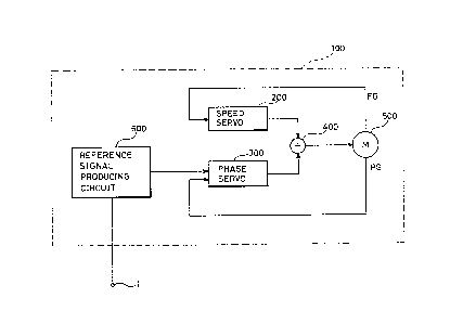
Fig. 1 is a schematic block diagram of a motor servo
circuit for controlling rotation of a cylinder motor in a
VTR, employing a reference signal producing circuit, i.e.,
a synchronization separator circuit according to the
present in~ention. The same motor servo circuit is
further provided separately for controlling rotation of a
capstan motor in the VTR.
As shown in Fig. 1, a motor servo circuit 100
includes a speed servo circuit 200 and a phase servo
circuit 300. Control signals from these servo circuits
200 and 300 are added by an adder 400 and then applied to
a motor circuit 500. FG pulses and PG pulses detected in
the motor circuit 500 are fed back to the speed servo
circuit 200 and the phase servo circuit 300, respectively.
The motor servo circuit 100 also comprises a reference
signal producing circuit (a synchronization separator
circuit) 600 for generating a reference signal for the
phase servo circuit 300 in response to a composite
synchronizing signal inputted via an input terminal 1 from
a video circuit which is not shown. Such speed and phase
servo is usually realized on a software manner by a
l~D9~75
microcomputer, as described in, for example, Sanyo
Technical Review Vol. 19 No. 2, 1987, pp. 18-24.
Next, a description will be given on a configuration
of the reference si~nal producing circuit according to one
embodiment of the present invention with reference to Fig.
2.
~ s shown in Fig. 2, a composite synchronizing signal
a inputted from the external video circuit via the input
terminal 1 is applied to a counter 3 via a shaping
amplifier 2. The counter 3, which performs up/down
operation controlled depending on the level of the
composite synchronizing signal outputted from the shaping
amplifier 2, up-counts clock pulses of 4 MHz when the
composite synchronizing signal is a.t the H level and
down-counts the same at the L level.
A count value b of the counter 3 is applied to
respective output compare registers OCRHD4 and OCRVD5 for
horizontal detection and for vertical detection. Each of
these output compare registers generates a pulse which is
at the H level during a fixed period when its input
exceeds its set value. In further detail, the OCR~D4
outputs a pulse at the H level when the:count value from
the coun~er 3 reaches a value corresponding to 2.75 ~ sec,
while the OC~VD5 outputs a pulse at the H level when the
count value reaches a value corresponding to 17 ~ sec. An
i 1 ~09 1 ~5
output (Fig. 3(c)) from the OCRHD4 is applied to a
horizontal processing block 6, and an output (Fig. 4(c))
from the OCRVD5 is applied to a vertical processing block
7. The reference signal producing circuit 600 further
includes a PAL/NTSC decision block 8 and an even/odd
number field decision block 9.
Th~ horizontal processing block 6 comprises an AND
gate 10, an RS-flip-flop 11 for HD mask, an OR gate 12, a
horizontal timer counter 13 for counting clock pulses of
4MHz and being reset by an output of the OR gate 12,
horizontal outpu~ compare registers OCRH14, 15, 16 and 17,
an H50 output RS-flip-flop 18 for outputting a horizontal
synchronization period signal of 50~ duty, and a *H output
RS-flip-flop 19 for outputtin~ a horizontal ..
synchronization period signal having a pulse width of 4.75
sec employed as a quasi vertical synchronizing signal.
Each of the OCRH14, 15, 16 and 17 receives an output
of the horizontal timer counter 13 to generate a pulse
which attains the H level during a fix period when its
input exceeds its set value. In more detail, ~he OCRH14
has a set value corresponding to 102% of a normal
horizontal period; the OCRH15 has a set value
corresponding to 90~ of the:normal horizontal period; the
OCRH16 has a set value corresponding to 50% of the normal
horizontal period; and the OCRH17 has a set value
_ g
13~9175
corxesponding to a pulse ~idth of a normal horizontal
synchronizing signal.
An output of the OCRH 14 is supplied as a horizontal
synchronizing signal for compensation to one input of the
OR gate 12. An output of the OCRH15 resets the
RS-flip~flop 11 for HD mask. An output of the OCRH16
resets the H50 output RS-flip-flop 18. An outp~lt of the
OCRH17 resets the *H output RS-flip-flop 19. The AND gate
10 receives an output c from the OCRHD4 and a Q output of
the RS-flip-flop 11 for HD mask to generate an output e
and supply the same to the other input of the OR gate 12
and to a set input of the RS-flip-flop 11 for HD mask.
The output of the OR gate 12 is outputted as an H signal
and also sets the H50 output RS-flip-~lop 18 and the *H
output RS-flip-flop 19.
Meanwhile, the vertical processing blocX 7 has a
configuration similar to the above described horizontal
processing block 6~ That is, the vertical processing
block 7 comprises an AND gate 22, an RS-flip-flop 24 for
VD mask, an OR gate 23, a vertical timer counter 25 for
counting clock pulses of 2MHz and being reset by the
output of the OR gate 23,;vertical output ~ompare
registers OCRV26, 27, 28 and 29, which correspond to the
AND gate 10, the RS-flip-flop 11 for HD mask, the OR gate
, . . .
`' 130ql7,~
12, the horizontal timer counter 13, and the OCRH 14 to
17, respectively.
In addition to these elements, the vertical
processing block 17 further comprises an AND gate 30
allowing an external input VEI to enter, an OR gate 31 for
obtaining a set input of the RS-flip-flop 24 for ~D mask,
an RS-flip-flop 32 for VD compensation, an RS-flip-flop 33
for output forbidding, an AND gate 34, and an RS-flip-flop
35 for external VD detection.
Each of the OCRVs 26, 27, 28 and 29 receives an
output of the vertical timer counter 25 to generate a
pulse whicil attains the H level during a fixed period when
its Lnput exceeds its set value. In fur~her detail, the
OCRV26 has a set value corresponding to 102% of the normal
vertical period. However, the set value is changed to a
value corresponding to the normal vertical period in the
case that the vertical synchronizing signal pulses lack
over a long period of time, as will be described later.
Moreover, a value for determining timing of even/odd
number field decision, which will be described later, is
set in the OCRV27. This timing is slightly delayed from
the timing of an output of~the AND gate 22. A value is
set in the OC~V28, which determines a period to forbid
inputting of a signal immedlately after compensation of
the vertical synchronizing signals. This set value is 5m
1309175
sec in an NTSC system and is 6m sec in a PAL system. A
value is set in the OCRV29, which determines a mask period
(of 15m sec in the NTSC system and of 18 m sec in the PAL
system).
An output of the OCRV26 is supplied to one input of
the OR gate 23, a set input of the RS-flip-flop 32 for
detecting VD compensation, and to a set input of the
RS-flip-flop 33 for output forbidding. An output of the
OCRV27 is applied to the even/odd number fixed decision
block 9. An output of the OCRV28 is applied to a reset
input of the RS-flip-flop 33 for output forbidding and to
one input of the OR gate 31. An output of the OCRV 29 is
applied to a reset input of the RS-flip-flop 24 for VD
mask. The AND gate 22 receives an output c (Fig. 4) from
1~ the OCRVD5 and a Q output of the RS flip-flop 24 for VD
mask to generate an output and apply the same to one input
of the AND gate 30 t a reset input of the RS-flip-flop 32
for VD compensation and to the other input of the OR gate
31. The other input of the AND gate 30 is supplied with
an external signal VEI, and an output of the ~ND gate 30
is applied to the other input of the OR gate 23. An
output of the OR gate:31 is applied to a set input of the
RS-flip-flop 24 for VD mask. The AND gate 34 receives an
output of the OR gate 23 and:a Q output of the
-- 12 -
1 309 1 75
RS flip-flop 33 for output forbidding to generate a
reference signal REF 60 and output the same.
The RS flip-flop 35 for external VD detection has its
set input supplied with an output of the OCRVD5 ar,d its
reset input supplied with a clear signal generated in a
software manner by the microcomputer, which is not shown
in the figure. An output of this flip-flop 35 is employed
as an external VD detecting flag VEXF, which will be
described later.
Meanwhile, the PAL/NTSC decision block 8, which
decides that the video signal is provided in the PAL
system or in the NTSC system, and informs the
microcomputer of the result of this decision, is formed of
a counter ~0 for counting horizontal synchronizing signal
pulses outputted from the OR gate 12 as clock pulses and
being reset by the output of the OCRVD5, and a decision
output compare register 21 for receiving an output
thereof.
The even/odd number fieId decision block 9 formed of
D--flip-flops 36 and 37 decides which fleld is the present
field, and informs the microcomputer~of~the result of this
decision in the case that either the even number filed or
the odd number field is designated as a reference field
for performing phase servo. The D-flip-flop 36 latches
the level of a signal H50 with the output of the OCRVD5,
13 -
fl-3~ 5
and the D-flip-flop 37 latches a Q output of the
D-flip-flop 36 with the output of the OCRV27. A Q output
of the D-flip-flop 37 is supplied as a decision output.
Next, a description will be given on operation of the
5 horizontal processing block 6 in the reference signal
producing circuit shown in Fig. 2 with reference to the
timing chart of Fig. 3.
First of all, when the composite synchronizing signal
as shown in Fig. 3 (a) is inputted to the up/down counter
3 via the input terminal 1 and the shaping amplifier 2,
the counter 3 performs up-counting and down-counting when
the composite synchroniziny signal is at the H level and
at the L level, respectively, as shown in Fig. 3 (b).
When the count value of *he counter 3 increases to
reach the above described threshold value ~which
corresponds to 2.75 ~ sec), the OCRHD4 generates a pulse
of the H level having a fixed duration (see Fig. 3 (c))
and applies the same to one input of the AND gat~ 10.
However, no pulse occurs when the count value decreases to
reach the above described threshold value. The other
input of the AND gate 10 Ls supplied with a mask signal
from the RS-flip-flop 11 for HD mask, as shown in Fig. 3
(d). The RS-flip-flop 11 for HD mask is set by the output
of the AND gate 10 (see Fig. 3 ~e~) and is also reset by a
signal (see Fig. 3 (g)) outputted from the OCRH15, having
- 14 -
' 130ql75
a threshold value corresponding to 90% of the normal
horizontal period. Therefore, the mask signal d controls
opening/closing of the AND gate 10 to accept a signal c
only during the 10% period of the horizontal period. As a
result, the AND gate 10 is closed during the remaining 30
period of the horizontal period, resulting in removal of
noise components. An output e of the AND gate 10 is
outputted as a horizontal synchronizing signal (an H
signal) shown in Fig. 3 (~ and also applied to the
horizontal timer counter 13 via the OR gate 12. Since the
counter 13 is reset in the normal horizontal period in the
case of no lack of pulses of the signal e, the output of
the counter 13 does not reach a set value (which
corresponds to 102~ of the horizontal period) of the
OCRH14, so that no pulses occur in the output of the
OORH14 (see Fig. 3 (f)). In the case of lack of the
pulses of the signal e, however, the OCRH14 generates a
compensation signal f to apply the same to th~ other input
of the OR gate 12 at the time that the count value of the
counter 13 reaches the set value of the OCRH14.
Accordingly, the lack of the output e of the AND gate 10
is compensated, so that the compensated signal Q is
supp~ied as the H signal. In the case of successive lack
of the pulses of the signal e, the counter 13 is reset by
- 15 -
.
.
.
1309175
the output ~ of the OR gate 12, so that the output f of
the OCRH14 is employed as the compensation signal.
Meanwhile, the H50 output RS-flip-flop 18 is set by
the above described signal ~, and reset by an output of
the OCRH16 (see Fig. 3 (h)) having a set value
corresponding to 50% of the horizontal period. Therefore,
an output H50 thereof is illustrated as in Fig. 3 (j).
This horizontal synchronizing signal i f 50~ duty is
applied to the even/odd number fixed decision ~lock 9 for
even/odd number field decision, which will be described
later.
Further, the *H output RS-flip-flop 19 is set by the
above signal ~, and reset by an output of the OCRH17 (see
Fig. 3 (i)) having a set value corresponding to a pulse
width of the normal horizontal synchronizing signal.
Thus, an o~tput *~1 thereof becomes a signal having a pulse
width of 4.75 ~ sec, as sho~l in Fig. 3 (k), to be
employed as a horizontal period synchronizing signal in
the special reproducing as described above.
~ description will now be given on operatLon of the
vertical processing block in the reference signal
producing circuit shown in Fig. 2 with reference to the
timing charts of Figs. 4 through 6.
First of all, waveforms shown in Figs. 4 (a) and (b)
are identical to those of Figs. 3 (a) and (b) in the
- 16 -
1309175
foregoing. That is, Fig. 4 (b) represents the count value
of the up~down counter 3. When this count value increases
to reach the above described threshold value ~which
corresponds to 17 ~ sec), the OCRVD5 generates a pulse of
the H level having a fixed duration (see Fig. 4 (c)) and
apply the same to one input of the AND gate 22. However,
no pulses occur when the count value decreases to reach
the above described threshold value. Thus, the horizontal
synchronizing signal and the vertical synchronizing signal
are separated by setting the threshold value of the OCRHD4
to 2.75 ~ sec and that of the OCRVD5 to 17 ~ sec. These
threshold values may be set to 3.5 ~ sec and ~4 ~ sec,
respectively.
Fig. 5 is a timing chart for illustrating operation
Of the vertical processing block 7 in the case of no lack
of the vertical synchronizing signal pulses. The AND gate
22 has its one input supplied with a vertical
synchronizing signal ~see Fig. 5 (a)) separated by the
OCRVD5, as described above, and the other input supplied
with a mask signal as shown in Fig. 5 (b3 from the
RS-flip-flop 24 for VD maskO The~RS-flip-flop 24 for VD
mask is set by an output of the OR gate 31 and also reset
.:
by a signal (see Fig 5 (d)) from the OCRV29 having a
predetermined set value determining a mask period.
Therefore, the mask signal (see Fig. 5 ~b~) controls
17 -
:
)9 1 7~i
opening/closing of the AND gate 22 such that the gate is
- closed only during the period o~ 15m sec in the NTSC
system and of 18 m sec in the PAL system after the
vertic~l timer counter 25 is reset by the vertical
synchronizing signal.
An output of the AND gate 22 is supplied to the OR
gate 23 via the AND gate 30, and an output of the OR gate
23 (see Fig. 4 (c)) is outputted as the reference signal
REF 60 via the AND gate 34. In the case of no lack of the
vertical synchronizing signal pulses, the count value of
the vertical timer counter 25 does not reach a set value
(which is 102% of a vertical period) of the OCRV26, and
thus the RS-flip-flop 33 for output forbiddin~ is not set.
Therefore, the AND gate 34 is not closed, so that the
output of the OR gate 23 (Fig. 5 (c)) is outputted as a
reference signal. In this case, an output of the OCRV28
(Fig. 5 (e)) does not function.
Fig. 6 is a timing chart for illustrating operation
of the vertical processing block 7 in the case that lack
or delay occurs in the vertical synchronizing signal
pulses.
That is, since the vertical timer~counter 25 is not
reset in the normal vertical synchronizing period in the
case that a lack occurs in the vertical synchronizing
~i~nal pulse, as shown by the broken line of Fig. 6 (a),
- 18 -
1 ~ 0 9 1 7 ~
an output shown in Fig. 6 (c) is obtained from the OCRV26
having a set value corresponding to 102% of the vertical
period. That is, the timing of the output of the OCRV26
is deviated by 2~ of the ~ertical period from the timing
of the original vertical synchronizing period. The output
of the OCRV26 is supplied as the compensation signal to
the OR gate 23, thereby compensating the lack of the
output of the AND gate 22. The lack of the vertical
synchronizing signal pulse does not cause the RS-flip-flop
24 for VD mask to be set, so that the mask period does not
start. Therefore, by setting the RS-flip-flop 24 for VD
mask by an output of the OCRV28 (Fig. 6 (e)), the mask
period is forced to start. (Fig. 6 ~b)).
Furthermore, the output of the OCRV26 sets the
RS-flip-flop 32 for VD compensation and the RS-flip-flop
33 for output forbidding. The RS-flip-flop 32 for VD
compensation is reset by the output of the AND gate 22,
and an output VINL thereof (Fig- 6 (g)) informs the
microcomputer that compensating operation is carried out.
The RS-flip-flop 33 for output forbidding is reset by the
output of the OCRV28, and an output thereof (Fig. 6 (f))
is supplied to the other input of the ~ND gate 34.
Accordingly, the AND gate 34 is closed during a fixed
period immediately af~er the compensating operation is
carried out.
- 19 -
~ 1309175
In the case that there is no lack of the vertical
synchronizing signal pulses, but the vertical period
increases temporarily for some reason and then returns to
the original period (shown by the broken line of Fig. 6
(d)), the RS-flip-flop 33 and the AND gate 34 forbid
outputting which occurs immediately after the compensating
operation, as described above, thereby preventing delayed
vertical synchronizing signal pulse from being outputted
~Fig. 6 ~h)) and thus occurrence of an output of an
extremely short period.
In the case that a predetermined number or more of
the vertical synchronizing signal pulses lack successively
for some reason, the set value of the OCRV26 is
automatically varied by the microcomputer. Fig. 7 is a
flow chart illustrating an operation of varying this set
value.
As shown in Fig. 7, each time the reference signal
REF 60 is provided from the AND gate 34, an interrupt
operation ~step S38) is performed as follows.
First of all, the level of the VEI externally applied
is checked (step S393. The VEI here represents a signal
which attains the H level in recording in the VTR and the
L level in reproduction. When the VEI~is at the H level
(or "l"), the level of V}NL being a Q output of the
RS-flip-flop 32 for VD compensation is checked (step S40).
- 20 -
i 1 ~09 1 75
If the vI~L is at the L level, i.e., if the compensating
operation of the vertical synchronizing signal pulses is
not carried out, a register REFCNT is reset (step S41) to
complete the interrupt operation (step S42).
Meanwhile, since the compensating operation of the
vertical synchronizing signal is carried out when the VINL
is at the H level, the value of the register REFCNT is
incremented by one (step S433, so that it is checked
whether or not the value of the REFCNT is larger than 4
(step S~4). If the value is not larger than 4, the
interrupt operation is completed (step S45).
On the other hand, if the value is larger than 4, the
VEI is reset (step S46), and then the REFCNT is reset
(step S47). The set value of the OCRV26 is then set to a
value equal to that of the vertical synchronizing period
(step S48) and then the interrupt operation is completed
(step S49).
In addition, when the VEI is at the L level (or "0"),
the VEXF which is a Q output of the RS-flip-flop 35 for
external VD detection is checked (step S50). If the VEXF
is at the L level, the register REFCNT is reset (step S51)
since there is no external input, and then the interrupt
operation is completed (step S52).
On the other hand, when the VEXF is at the H level,
the value of the REFCNT is incremented by one (s~ep S53
- 21 -
~ 3~9 1 75
to clear the VEXF (step S54) and then check whether or not
the value of the REFCNT is larger than 4 (step S55). If
the value is not larger than 4, the interrupt operation is
completed (step S56).
If the value is larger than 4, the VEI is set (step
S57) and the REFCNT is reset (step S58~, so that the set
value of the OCRV26 is set to be 102% of the vertical
synchronizing period (step S59) to complete the interrupt
operation (step S60).
Due to the above descri~ed interrupt operations,
unless four or more of the vertical synchronizing signal
pulses are inputted successively when the VEI = 1, namely,
in the state of accepting an external input, an internal
reference signal having the normal vertical period is
selected to be outputted. Meanwhile, if four of the
vertical synchronizing signal pulses are successively
inputted externally when the VEI = 0, namely, in the state
of employing an internal reference signal, the external
input is selected to be outputted. A timing chart of Fig.
8 illustrating the above described operatlons, shows the
case that a change to the internal reference signal is
available with the lack of two or mo~e of the vertical
synchronlzlng signal pulses, for brief description
thereof.
- 2~ -
. .:, . . :
i 1 30q 1 75
Meanwhile, a similar operation is performed with
respe~t to the horizontal synchronizing signal. Namely,
in the case that a predetermined number or more of the
horizontal synchronizing signal pulses lack successively
for some reason, the set value of OCRH14 is automatically
varied by the microcomputer to correspond to the normal
horizontal period.
Decision of the PAL/NTSC by the PAL/NTSC decision
block 8 is carried out based on the number of the H signal
pulses to be counted before the counter 20 is reset by the
output of the OCRVD5. That is, 312.5 of and 262.5 of the
H signal pulses should be counted in the PAL and NTSC
systems, respectively, because of a difference in number
of scanning lines between these two systems. Therefore, a
threshold value of the OCR21 is set to 288, so that an
output thereof decides the PAL~NTSC. The result of this
decision makes the set values of the respecti~e OCRs
varied.
Furthermore, the even/odd number field decision block
9 carries out the decision of the even/odd number fields
based on the level of the H50 signal (b) in rising of the
output of the OCRVD5 (Fig. 9 ~c) and Fig. 10 (c)), i.e.,
based on a difference in phase relationship between the ~
50 signal and the vertical horlzontal signal, as shown in
Figs. 9 and 10. For example, as shown in Fig. 9, if the
- 23 -
.
11 3 (~ 9 1 ~5
H50 signal (b) is at the H level in rising of the output
(c) of the OCRVD5, the ~lock 9 decides on the odd number
field (d). Meanwhile, as shown in Fig. 10, if the H50
signal (b) is at the L level in rising of the output (c)
of the OCRVD5, the block 9 decides on the even number
field (d). A delay due to the OCRV27 is not inherent
processing but for synchronizing the timing of other
processing with each other.
Next, a description will be given on the reference
signal producing circuit according to the second
embodiment of the present invention with reference to Figs
11 and 12. The second embodiment is the one to solve the
following problems which occur in the horizontal
processing block of the above described first embodiment.
That is, in the synchronization separator circuit in
Fig. 2, when the original horizontal synchronizing signal
pulse is inputted immediately after compensation of the
horizontal synchronizing signal pulse by the OCRH14 (Fig.
12 (a)), for example, in changing the channel, the *H
signals are successi~ely output~ed in an extremely short
period (d). Further, when the lack of the horizontal
synchronizing signal pulse is compensated, masking of the
HD signal is not carried~out in the configuration o Fig.
~ tFig. 12 (b)). Therefore, noise is liable to be
regarded as the horizontal s~nchronizing signal pulses.
_ 24 -
'~
1 309 1 75
In consideration of the foregoing problems, the
embodiment of Fig. ll is configured such that the
RS-flip-flop 19 for ~H output is se-t by a Q output of the
RS-flip-flop 18 for H50 output, and also the H50 signal is
employed as a clock signal of the PAL/NTSC decision block
8. ~he employment of this stable H50 signal keeps both
the state of the RS-flip-flop 18 for H50 output and thus
the *H signal unchanged, even if the original horizontal
synchroni2ing sig~al pulse is inputted immediately after
compensation of the lack of the horizontal synchronizing
signal pulse. Thus, the PAL~NTSC decision can also be
carried out more accurately.
Moreover, the embodiment of Fig. 11 is further
configured such that an OCRH70 is separately provided
having a set value corresponding to 25.5 ~ sec, and the
RS-flip-flop ll for HD mask is set by an output of the
OCRH70 or that of the AND gate 10. Accordinqly, the AND
gate 10 is masked (Fig. 12 (g)) when 25.5 ~ sec have
passed after compensation of the lack of the horizontal
synchronizing signal pulse, so that noise is less liable
to be regarded as the horizontal synchroniziny signal
pulse.
As has been described, according to the embodiments
of the present invention, the stable phase servo control
can be carried out by making equal the period of the
- 25 -
I ~Oq J 75
compensation signal to the vertical synchronizing period,
in the case that the plurality of vertical synchronizing
signal pulses lack successively. Furthermore, even in the
case that the plurality of the horizontal synchronizing
signal pulses lack, the occurrence of the V jitter in
special reproducing can be prevented by compensation of
this lack.
Although the present invention has been described and
illustrated in detail, it is clearly understood that the
same is by way of illustration and example only and is not
to be taken by way of limitation, the spirit and scope of
the present invention being limited only by the terms of
the appended claims.
- ~6 -