Note : Les descriptions sont présentées dans la langue officielle dans laquelle elles ont été soumises.
1 ~ 7
SELF REGULATING TEMPERATURE HEATER
WITH THERMALLY CONDUCTIVE EXTENSIONS
The present -invention relates to a method and
apparatus for soldering a first plurality of electrical
contacts to a second plurality of electrical contacts.
The invention has particular utility in ~oining flexible
etched cables, ribbon cables and surface mount connectors
to contact pads on printed circuit boards and may also be
employed to join two single contacts instead of
pluralities of contacts.
Although the invention has its primary utility in
simultaneously joining first and second pluralities of
contacts, it will be appreciated that the principles
described herein are equally applicable to joining a
single contact to another single contact. Moreover,
although the description set forth below mentions solder
as the joining material, it is to be understood that any
fusible material, such as doped conductive plastic
material, may be employed.
Soldering flat cable leads to circuit board contact
pads can be achieved by a -~ariety of prior art methods and
apparatus. The least desirable of these is manually
effecting each of the multiple solder terminations because
the resulting repetitive soldering operations are
time-consuming and costly. In addition, close spacing
between adjacent connection sites renders it likely that
14321 CA -1-
`` 13~ L37
one or more of the manual soldering operations wi~l result
in solder bridges between one or more pairs of the
adjacent sites.
There have been a number of prior art attempts to
solve the aforementioned problems, examples of which may
be found in U.S. Patent Nos. 3,396,894 (Ellis), 3,719,9~1
(Steitz), 3,750,252 (Landman) and 4,484,704 (Grassauer et
al). Typically, in thess ancl other prior art soldering
procedures for forming multiple solder joints
simultaneously, a soldering tool is employed to deliver
the necessary thermal energy over a large continuous area
spanning all of the connection sites. Upon energization,
the soldering tool heats up until it overshoots a control
temperature before settling down to that temperature. The
control temperature is typically chosen somewhat above the
ideal soldering temperature in order to compensate for
less than ideal thermal energy transfer. This approach to
thermal energy delivery has a number of disadvantages. One
such disadvantage is damage to components resulting from
overheating. For example, the thermal overshoot inh~rent
in the heating tool can damage components disposed between
the connection sites within the area heated by the tool.
In some cases the overshoot may cause damage to the
polymeric materials, insulating materials and adhesives at
the connection site. It is tempting to suggest that the
operator of the soldering tool might avoid the thermal
14321 CA -2-
overshoot by either removing the tool be~ore the overshoot
occurs or delaying application of the tool until after the
overshoot occurs. This is impractical for a number of
reasons. First, there is no evident indication as to when
the thermal ovsrshoot occurs. Second, although the tool
warm-up time is quite long, the time interval during which
the tool temperature is suf~Eicient to melt solder, but
prior to overshoot, is too,short to reliably complete the
soldering operation. Further, where the tool is also
employed to apply pressure to the connection site, the
power must be turned off after the solder m~lts while
pressure is maintained on the tool until the solder
solidifies. The tool must be re-energized to e~fect the
next soldering cycle. The repeated on-off cycling changes
the starting temperature for the transient overshoot in
each cycle, thereby making it virtually impossible to
determine when the tool attains the final control
temperature.
Another prior art problem associated with the
simultaneous soldering of sets of plural contacts relates
to solder bridging between connection sites. The
pressure and thermal energy applied to spaces between
~onnection sites tends to cause the solder to run between
those sites and ~orm solder bridges. This problem has
been addressed in some prior art apparatus such as that
disclosed in the aforementioned Grassauer et al patent.
14321 CA -3-
In that apparatus the solder is sandwiched between two
layers of polymeric matarial, one of which has window
openings arranged to permit the solder, when melted, to
flow through to respective connection sites. Barriers are
provided between the windows to preclude solder bridging.
While this technique minimizes bridging when properly
employed, proper employment is hampered by the difficulty
of aligning the windows (which must necessarily face
downward and away from the technician) with respective
contact pads at the connection sites. Care must also be
taken to avoid displacement of the solder within the
layered polymeric package prior to heating the apparatus
in order to assure that sold~r is present at each of the
window openings.
It is desirable, therefore, to provide a method and
apparatus that permits simultaneous soldering at multiple
connection sites without applying thermal energy to spaces
between those sites and without creating solder bridges
between adjacent connection sites. Moreover, the method
and apparatus should be equally useful in joining a single
contact to another single contact. In addition, it is
desirable that the thermal energy required to melt the
soider be available virtually instantaneously after en0
ergization of the heater, and that the heater be arranged
to provide no more thermal energy than is required to melt
the solder employed for the various connection sites.
14321 CA -4-
~ 3 ~ 7
~ 7789-272
Finally, it is desirable that the apparatus have relatively low
mass in order that it may cool down quickly after a soldering
operation.
The present invention makes use of a relatively new
automatic self~regulating heater technology disclos2d in U.S.
Patant Nos. 4,256,945 (Carter et a:L), 4,623,401 (Derbyshire et
al), 4,659,912 (Derbyshire), 4,695,713 (Krumme), 4,701,587 (Carter
et al), 4,717,81~ (Krumme) and 4,745,2~4 (Carter). A heater
constructed in accordance with that technology, hereinafter
referred to as a self-regulating heater, employs a substrate of
copper, copper alloy, or other material of low electrical
resistivity, negligible magnetic permeability and high thermal
conductivity. A thin layer of thermally-conductive magnetic
material is deposited on all or part of one surface of the
substrate, the layer material typically being an iron, nickel or
nickel-iron alloy~ or the like, having a much higher electrical
resistance and magnetic permeability than the substrate material.
The thickness of the layer is approximately one skin depth, based
on the frequency of the energizing current and the permeab-ility
and resistance of the layer. A constant amplitude, high frequency
alternating energizing current is passed through the heater and,
as a
:,
- .
.
:.
-` 1 3 ~ 7
result of the s~in effect phenomenon, is initially
concentrated in one skin depth corresponding to the
thickness of the magnetic material. When the temperature
at any point along the heater reaches the Curie
temperature of the magnetic material, the magnetic perme0
ability of the magnetic material at that point decreases
dramatically, thereby significantly increasing the skin
depth so that the current density profile expands into the
non-magnetic substrate of low resistivity. The overall
result is a lower resistance and lesser heat dissipation.
If thermal sinks or loads are placed in contact with the
heater at different locations along the heater length,
thermal energy is transferred to the loads at those
locations with the result that the temperature does not
rise to the ailoy Curie temperature as quickly at those
locations as it does in the non-loaded locations. The
constant amplitude current remains concentrated in the
higher resistance alloy layer at the loaded locations
which dissipate considerably more resistive heating energy
than is dissipated in the non-load locations where the
current is distributed in the low resistance substrateO
In accordance with the present invention,
self-regulating temperature heater provides sufficient
~ s ~ bl~z
thermal energy to melt a ~e conductive material and
thereby provide an electrically- conductive connection
between a first electrical contact and a second electrical
14321 CA -6-
~3~37
677~9-272
contact. The heater comprises a selectively actuable heater body
for supplying at least said sufficient thermal energy, said heater
body comprising a substra~e of an electrically-conductive first
material having a relatively low electrical resistivity and
relatively low magnetic permeability, said substrate having a
first surface, and a skin layer of an electrically-conductive
second material disposed on at least a portion of said first
surface, said second material having a higher electrical
resistivity than that of said first material, and having a
magnetic permeability which at temperatures below its Curie
temperature is substantially greater than said relativel~ low
magnetic permeability and at temperatur0s above its Curie
temperature is substantially the same as said relatively low
magnetic permeability; a thermally-conductive connecting mamber
secured to and in thermally-conductive contact with said heater
body and adapted to be disposed in both electrical and thermal
contact with and physically between said first contact and said
second contact to transfer said sufficient thermal energy to said
first and second contacts from said heater body and to remain a
permanent part of the electrically-conductive connection between
the first and second contacts; and said apparatus further
comprising means for selectively causing alternating current to
flow in said heater body at a substantially fixed amplitude
sufficient to heat said skin layer to its Curie temperature within
a prescribed time interval and at a frequency such that the
current in the region of said portion of said first surface is
concentrated ln said :kin layer.
~,
~31~7
677~9-~72
According to another aspect, the invention provides a
method for providing electrica:Lly-conductive connections between
contacts in a first plurality of spaced electrical contacts and
respective contacts in a second pluralit~ of similarly spaced
electrical contacts at a respective plurality of connection sites,
said method comprising the steps of: disposing a plurality of
connec~ing members at respective connection sites in abutting
relation with a respective contact in said ~irst plurality of
contacts and a respective contact in said second plurality of
contacts, each of said connecting members projects from and is in
thermally-conductive contact with a heater body having a substrate
of an electrically-conductive ~irst material having relatively low
electrical resistivity and magnetic permeability, and a skin layer
of second material haviny a very much higher magnetic permeability
at temperatures below its Curie temperature and a ~reater
electrical resistivity than that of said fixst material;
delivering thermal energy to said connection sites via said
; connecting members to melt fusible electrically-conductive
material at each connection site by flowing an alternating current
of fixed ampli.tude in said heater body such that, (a) for heater
body temperatures below the Curie temperature of said second
material the current is substantially concentrated in said sXin
layer; and (b) for heater body temperatures above sald Curie
temperature the current is distributed to a substantially ~reater
extend in said substrate; and removing the thermal energy from the
connection sites to permit the fusible material to harden and
secure said first and second pluralities of contacts to said
7a
; .
~31~ 7
~ 7789-27~
plurality of connec~ing members whereby each connecting member
remains a permanent part of a respective e:Lectrically-conductive
connection at a respective connection site.
7b
::`
' `; ~ ,
3 7
The invention will now be described by way of example
with reference to the accompanying drawings, in which:
FIGURE 1 is a view in perspective of a heater
assembly with severable connecting members projecting
therefrom in accordance with the present invenkion;
FIGURE ~a is a view in transverse section of the
assembly of Figure 1 showing that assembly employed for
soldering a flexible etched cable to contact pads on a
printed circuit board;
FIGURE 2b is a view in longitudinal section taken
along lines b-b of Figure 2a with electrical connections
to the heater assembly schematically illustrated;
FIGURE 3 is a view in transverse section similar to
Figure 2a but showing the heater assembly broken away fxom
the connecting members after soldering;
FIGURE 4 is a view in transverse section similar to
Figure 2a showing the heater assembly o:E Figure 1 employed
in conjunction w.ith a removable tooling bar;
FIGURE 5 is a view in perspective of an alternative
heater assembly with severable connecting members
projecting therefrom in accordance with the present
: invention;
FIGURE 6 is a view in perspective of another
embodiment of the present invention including a heater
assembly with severable connacting members;
14321 CA -8-
FIGURE 7 is a view in transverse section taken along
lines 7-7 of Figure 6;
FIGURE 8 is a view in perspective of another
embodiment of a heater assembly and projecting connecting
members constructed in accordance with the principles of
the present invention;
FIGURE 9 is a view in transverse section taken along
lines 9-9 of Figure 8;
FIGURE 10 is a partially schematic view in
perspective of an alternative embodiment of the present
invention;
FIGURE 11 is a view in longitudinal section of
another embodiment of the present invention;
FIGURE 12 is a view in perspective of an alternative
embodiment of a heater assembly of the present invention
shown in position for soldering the solder tails of a
surface mount connector to contact traces on a printed
circuit board;
FIGURE 13 is a view in perspective of the heater
assembly of Figure 12 shown in position for soldering a
ribbon cable to contact traces on a printed circuit board;
FIGURE 14 is a view in perspective of a heater
assembly having flexible connecting members projecting
therefrom in accordance with an alternative embodiment of
the present invention;
14321 CA -9-
FIGURE 15 is a view in perspective of an alternative
heater assembly having severable projecting connecting
members constructed in accordance with the present
invention;
FIGURE 16 is a view in transverse section of the
assembly of Figure 15 showing that assembly employed for
soldering a flexible etched cable to the contact pads on a
printed circuit board;
FIGURE 17 is a view in transverse section of the
assemblies of Figures 1 and 7 employed on opposite sidPs
of a printed circuit card to solder respective sets of
contacts of a card edge connector to contact pads on the
card;
FIGURE 18 is a view in transverse section of two
self-regulating heater assemblies employed in mutually
interactive relation for soldering respective sets of
contacts of a card edge connector to contact pads on a
printed circuit card; and
FIGURE 19 is a view in perspective of an alternative
form of heater assembly having severable connecting
members projecting therefrom in accordance with the
present invention.
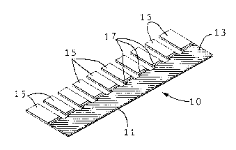
Referring specifically to Figure 1 of the
accompanying drawings, thare is illustrated an apparatus
10 for use in soldering one set of contacts to another get
of conta¢ts. The apparatus includes an elongated
14321 CA -10-
rectangular substrate 11 of copper or other material
haviny a high electrical conductivity (i.e., low
resistivity) and negligible magnetic permeability (i.e., a
permeability of, or close to, one). The substrate
material must also be a good thermal conductor. Substrate
11 typically, although not necessarily, has a length much
greater than its width which, in turn, is much greater
than its thickness. As an example of these relative
dimensions, the substrate length may be three inches, its
width may range from one-tenth to one-half inch, and its
thickness may be 0.002 inch. It should be noted that the
rectangular substrate configuration illustrated in Figure
1 is merely an exemplary configuration and that
substantially anv configuration, consistent with the
principles described herein, may be employed.
A thermally-conductive layer 13 of magnetic material
is deposited or otherwise disposed over one surface of
substrate 11. In the illustrated embodiment layer 13 is
disposed over the entirety of that surface but, as
described below, may be disposed only on selected surface
portions. A typical material for layer 13 is nickel-iron
alloy, such as Alloy 42 (42% nickel, 58% iron), or Alloy
42-6 (42% nickel, 6% chromium, 52% iron); however, layer
13 may be any metal or alloy having the characteristics
described herein. Depending upon the particular material,
magnetic permeabilities for layer 13 range from fifty to
14321 CA -11-
~ 3 ~ 7
more than one thousand, as compared to a permeability of
one for copper; typical electrical resistivities for layer
13 range from twenty to ninety micro-ohms per centimeter
as compared to 1.72 for copper. The thickness of layer 13
is typically one skin depth. In this regard, substrate 11
and layer 13, when energizled by passiny a constant
amplitude alternating current therethrough, function as a
self-regulating heater. Specifically, for temperatures
below the Curie temperature of the material of layer 13,
slightly more than sixty-three percent of the constant
amplitude current flowing through the heater is
concentrated in one skin depth from the heater surface.
The skin depth is proportional to the square root of the
material resistivity, and is invarsely proportional to the
square root o~ the product of the magnetic permeability of
layer 13 material and the frequency of the alternating
current passing through the heater. At temperatures equal
to or above the Curie temperature of the layer 13
material, the magnetic permeability of the material drops
to approximately that of the substrate material (i.e., a
permeability of one, for copper), thereby producing a
dramatic increase in the skin depth. Consequently, much
more of the constant amplitude current is distributed in
the lower resistivity substrate 11 than in higher
resistivity layer 13, with the result that considerably
less heat is dissipated. Importantly, if selected
14321 CA -12-
1 3 ~ 7
locations of the heater body are in contact with thermal
energy absorptive loads (e.g., heat sinks), then the
temperature at those locations of the heater body does not
rise as readily as it does at the non-load locations. It
is possible, th~refore, for the constant amplitude current
to be concentrated in layer 13 to a greater extent at the
load locations (where the temperature is below the Curie
temperature for layer 13) than at the non-load locations
(where the temperature is equal to the Curie temperature
of material 13). Curie temperatures for materials can
range from 50C to 1000C; typical materials employed for
layer 13 have Curie temperatures in the range of 200C to
5000C, depending on the solder or fusing material
employed.
A plurality of thermally and electrically conductive
connecting members 15 project from the heater body. In
the embodiment illustrated in Figure 1, there are ten
connecting members 15 projecting from a common edge of the
heater body in spaced parallel relation. The spacing
between the connecting members 15 is determined by the
spacing between contact pairs to be joined by soldering,
as described below. Likewise, tha configurations of the
connecting members 15 are determined by the configurations
of the contacts to be joined. In the illustrated
embodiment the spacing is the same between each pair of
adjacent connecting members, and the configurations of the
14321 CA -13-
3 7
connecting members are identical. In particular,
connecting members 15 are finger-like projections of
sufficient rigidity to retain their shape when suspended
in cantilever fashion from the heater body. Importantly,
each connecting member 15 is in thermally-conductive
relation with the heater body so that each membar 15 may
conduct thermal energy developed in the heater body to a
respective connection site where a soldering operation is
to be performed. The connecting members may be formed by
stamping, or the like, as integral parts of the substrate
11, in which case the thickness of each connscting member
15 may be on the same order of magnitude as the thickness
of the substrate. Of course, the thickness of the
connecting members may be greater or less than the
thickness of the substrate.
An important aspect of this embodiment of the
invention resides in the fact that conne~ting members 15
may be readily severable from the heater body after a
solder operation has been completed. Accordingly, each
connecting member 15 is provided with a notch 17 extending
transversely across the member and to a sufficient depth
to permit the heater body to be broken away from the
members 15 by bending, tearing, etc. Alternatively, the
connecting members 15 may be scored, perforated or
otherwise weakened in torsional strength to facilitate
their separation from the heater body.
,
14321 CA 14-
- ', '
'
;-
Referring to Figures 2a and 2b of the accompanyingdrawings, heater assembly lo is illustrated as being
utilized to solder conductors 21 in a flexible etched
cable 20 to respective contact pads 23 on a printed
circuit board 19. Although only a single cable conductor
21 and a single contact pad 23 are visible in Figure 2a,
it is to be understood that plural spaced conductors 21
and spaced pads 23 are prov:ided, and that all of the
conductors 21 are to be soldered to respective contact
pads 23 simultaneously. Initially, at each connection
site, a finger-like connecting member 15 is placed on a
respective contact pad 23. It is assumed that the spacing
between connecting members 15 is the same as the spacing
betwaen contact pads 23, and that the con~iguration of the
connecting members is such that each member 15 contacts
its respective contact pad 23 without contacting any other
pad or circuit component on board 19. Each conductor 21
in cable 20 is then placed on a respective connecting
member 15. Thus, at each connection site there is flush
physical contact between the three stacked
electrically-conductive elements, namely, contact pad 23,
connecting member 15 and cable conductor 21.
In order to actuate the heater, a tooling assembly 30
is employed and comprises a conductive bus bar layer 25
and a superposed layer 27 of electrically insulative
material. The bus bar layer 25 is typically copper and
14321 CA -15-
,, ~ . i ., ~ ., .. :
, ?g ~
has dimensions similar to those of substrate 11.
Insulative layer 27 is typically Kapton and i5 slightly
larger in length and width than the corresponding
substrate dimensions; the thickness of layer 27 is of the
same order of magnitude as that of the substrate. The
tooling assembly 30 is secured flush against heater body
assembly 10 with the exposed surface of insulative layer
27 abutting the skin layer 13 of the heater body. The
heater body and tooling may be held together permanently
by adhesive between layers or any other technique that
joins the tooling to the heater body in flush abutting
relation.
As best illustrated in Figure 2b, a source 31 of
constant amplitude alternating current is connected in
series with an impedance matching circuit 33, and this
combination is connected across the heater body assembly
(at substrate 11) and the tooling assembly 30 (at bus bar
layer 25) at one end of the heater assembly. Source 31
may be any suitable constant amplitude alternating current
supply such as, for example, the source disclosed in U.S.
; Patent No. 4,626,767 (Clappier et al) and provides a
constant amplitude alternating signal, typically in the
radio frequency range. Most commonly, the frequency of
the actuating signal is 13.56 MHz. The constant amplitude
of the signal is selected to provide the desired heating
level. Impedance matohing circuit 33 serves to matrh the
14321 CA 16-
~ . . .
37
impedancs of the heater-tooling combination to the source
impedance.
At the end of the heater body located longitudinally
remote from the connection to source 31, there is a wire
35 or other short circuit interconnecting substrate 11 and
bus bar 25. Current flow through the heater, therefore,
at any instant of time, is in longitudinally opposite
directions in the heater 10 (i.e.,substrate 11 and layer
13), and bus bar 25. A resulting electric field is
established between heater 10 and bus bar 25 across
insulation layer 27, thereby concentrating the current
flowing through the heater assembly in the high resistance
surface layer 13 rather than in low resistance outer
surface of the substrate. The current flowing through bus
bar layer 25 is concentrated at the surface facing the
heater assembly 10. Since the current amplitude is
maintained constant, it is desirable, for optimal heating,
to concentrate the current in the higher resistance layer
13 of heater assembly 10 than in the low resistance
substrate 11. That is, the resistive heating, with the
current I maintained constant, is greater when the current
path has greater resistance R. The electric field,
developed by the oppositely directed current flowing in
heater assembly 10 and bus bar 25, assures that the
current in the heater assembly is concentrated in the high
; 14321 CA -17-
1 3 ~ 7
resistance surface region of the heater assembly facing
the bus bar.
As illustrated in Figure 2a, the thermal energy
resulting from resistive heating is conducted to the
various finger-like connecting members 15 in ~rder to melt
solder that is deposited in pre-determined amounts on one
or more of the conn~cting members 15, contact pads 23 and
conductors 21. In the preferred embodiment of the present
invention the distal end of each connecting member 15 has
solder deposited on both surfaces so that, upon actuation
of heater assembly 10, a solder fillet 37 is created
between conductor 21 and contact pad 23; solder fillets
also tend to form between conductors 21 and connecting
members 15, between connecting members 15 and contact pads
23, and between conductors 21 and contact pads 23. In
addition, small amounts of solder join abutting surfaces
of conductgrs 21 and connecting members 15, and join the
abutting surfaces of contact pads 23 and connecting
members 15. The result is a mechanically strong and
electrically conductive solder connection at each
connection site. The amount of solder deposited is
sufficient to effect the desired solder joint but
insufficient to result in solder bridging between
connection sites.
The nature of heater assembly 10 is such that the
resistive heating is produced only where it is needed to
14321 CA -18-
effect the soldering operations. More specifically, the
current through heater assembly 10 flows longitudinally
and thereby alternately encounters regions from ~hich
connecting members lS project and regions corresponding to
spaces between the connecting members 15. Thermal energy
developed in regions proximate the connecting members is
conducted to respective connlection sites by members 15,
thereby preventing the temperature at those regions from
building up quickly. On the other hand, in the regions
corresponding to the spaces between members 15, the
temperature increases rapidly until it reaches the Curie
temperature of the material of layer 13, whereupon the
effective skin depth is increased dramatically in those
regions. This causes more current to flow th~ough the low
resistance substrate material in these regions and, as a
consequence, less thermal energy is produced therein~ The
regions proximate connecting members 15 continue to
develop high amounts of thermal energy that is conducted
to the respective connection sites. Overheating of the
connection sites is prevented by the same mechanism; that
is, once the temperature at the connection site reaches a
certain level, thermal conduction from the heater to the
site ceases, thereby removi~g the heat sink effect o~ the
connection site. The thermal energy developed by the
current flowing in high resistance layer 13 then quickly
increases the temperature proximate the connecting memb~rs
14321 CA -lg
~ $~3~
15 until the Curie temperature of the material is reached.
At this point the effective skin depth along the entir~
length of the heater assembly is increased so that more of
the constant amplitude current flows through the low
resistance substrate 11 and significantly less thermal
energy is produced by resistive heating. After current is
removed from the heater assembly, the assembly begins to
cool and the solder is permitted to harden. The cooliny
proceeds quickly because the relatively low mass of the
heater does not retain its heat for long periods of time.
The heater assembly 10 and tooling 30 are broken away
from the severable connecting members 15 after the solder
hardens. This break-away operation is effected by bending
the heater and tooling relative to members 15 along the
linearly aligned notches or grooves 17 in the manner
illustrated in Figure 3. The connecting members 15 remain
a permanent part of the solder joint at each connection
site and provide a low-resistance current path between
conductors 21 and contact pads 23.
In the embodiment illustrated in Figure 4 a removable
tooling asse~bly 30a replaces the permanently secured
tooling assembly 30 illustrated in Figures 2a, 2b and 3.
An electrically conductive ground bar 25a has insulative
or dielectric layer 27a secured at one end thereof and
adapted to be placed flushed against skin layer 13 of
self-regulating heater assembly 10 ~hen a soldering
; 14321 CA -20-
'. . : . ,
~3~37
operation is to be performed. Ground bar 25a is
typically connected to electrical ground or common and is
re-usable with different heater assemblies to perform
multiple sequential soldering operations. A source 31
constant amplitude alternating current and a short circuit
connection 35 (see Fiqure 2b) are connected across
substrate ll and ground bar 25a in the manner described
above to perform a soldering operation.
Another self-regulating heater lOb is illustrated in
Figure 5. A substrate llb and skin layer 13b deposited or
otherwise overlying the substrate are similar to substrate
11 and skin layer 13, respectively, described above but
may have a cut-away interior portion 12 resulting in a
flat closed loop configuration about portion 12.
Energization of heater assembly lOb is effected by
inductive coupling through a generally U-shaped primary
circuit 30b having a source 31 of constant amplitude
alternating current connected across its ends. The
primary circuit 30b is typically part of the tooling
~ employed to perform a solderin~ operation and is removable
from the heater assembly. Primary circuit 30b, when
positioned for use, overlies heater assembly lOb and is
spaced from skin layer 13b by means of an insulative layer
(not shown) disposed on its bottom surfa~e and/or by an
air gap. Current flow through the primary circuit induces
eddy currents in the `heater assembly of sufficient
14321 CA -21-
~3~3~
magnitude to result in resistive heating required to
effect soldering operations at each of the connecting
members 15. It will be appreciated that the single turn
primary circuit 3Ob may be replaced by plural turns, such
as by winding plural turns of insulated wire about the
heater body either longitudinally or transversely (i.e.,
between connecting members 15 or through cut-away portion
12). In either case, inductive coupling from the primary
circuit induces eddy currents in the heater body to
lo raise the temperature of the connecting members 15 to the
desired soldering temperature.
Referring to Figures 6 and 7, self-regulating heater
lOc includes a substrate llc of generally rectangular
transverse cross-section having two magnetic skin layers
13c(1~ and 13c(2) deposited or otherwise disposed on
respective opposite surfaces corresponding to the larger
legs of the cross-section. The resulting three-layer
heater assembly lOc is energized for a soldering operation
by connecting a source 31 of constant amplitude
alternating current across its length at any of the three
layers.
The body of heater assembly lOc and its projecting
connecting members 15 are shown in the form of a carrier
strip with a series of longitudinally-spaced pilot holes
16 defined therethrough to simplify handling of the
carrier strip during fabrication and to facilitate
1~321 CA -22-
~3~37
alignment of the strip with various connection sites for a
soldering operation. If desired, a series of
longitudinally-spaced perforations 14 may extend widthwise
across the heater assembly body to permit each sequential
section of that body to be separated from the others along
with a corresponding connecting member 15 after
soldering operation. In this manner the individual
separated sections of the ~ea~ter body may remain permanent
parts of respective solder joints. In order to assure
against contact between the separated heater body
sections, two perforated lines may be provided between
each pair of separable body sections so that a short
length of body section may be discarded between each
section pair.
The use of the two magnetic skin layers 13~c)1 and
13(c)2, rather than just one skin layer, renders the
self-regulating feature of the heater more effective. In
particular, unless the current flow is otherwise
constrained, the skin effect tends to concentrate the
current at all of the surfaces of the substrate, not
merely the surface where the magnetic skin layer is
disposed. Thus, if the magnetic material is disposed only
on one surface of the substrate, the current flowing in
the skin depth of lower resistance material at the other
surfaces does not significantly contribute to the desired
resistance heating and is, therefore, substantially
14321 CA -23-
~ 3 ~ 7
wasted. Noreover, that current does not experience a
current distribution change (i.e., an incr~ase in skin
depth) at and above the Curie temperature of the maynetic
material and, therafore, does not contribute to
temperature self-regulation. Likewise, if the substrate
were to have a square transverse cross-section and two
surfaces were to have a magnetic skin layer, the desired
operation would not be efficiently attained. Ideally,
therefore, all of the surfaces of the substrate should be
lo coated with the magnetic skin layer to take maximum
advantage of the thermal self-regulation effects. As a
practical matter, a substrate having a rectangular
cross-section, and a width very much greater than its
depth, serves effectively as a self-regulating heater when
only the two larger surfaces are clad with the magnetic
skin layer. For example, substrate llc would typically
have a width that is at least fifty times greater than its
depth or thickness. Of course, in each application where
the current is substantially constrained to flow along one
surface, as where an electric field is established between
substrate ll and bus bar 25 (Figure 1), efficient
self-regulation is obtained even if only that surface is
clad with the magnetic skin layer.
Another embodiment in which heater body sections
remain permanent parts of the solder joints is illustrated
in Figures 8 and 9 to which specific reference is now
14321 CA -24-
, '
.
.
~3~ ~3~
made. The electrically and thermally conductive
connecting members 15d, instead of projecting from a
common heater body, are individual and separate
components. Each connecting member is bent back toward
itself at its proximal end to forrn a loop lOd serving as
the heater body. The connecting member loop lOd may be
open, as illustrated, with the proximal tip of the
connecting member spaced a small distance 18 from the
intermediate portion of the member; alternatively, the
loop may be closed (i.e., the proximal end may be bent to
abut the intermediate portion). A skin layer 13d is
deposited or otherwise disposed on the portion of each
connecting member facing interiorly of the loop. An
inductive heating tool 3Od includes an elongated conductor
25d surrounded by an insulative layer 27d. In order to
effect a soldering operation the heating tool 30d is
inserted through the proximal end loops lOd of each of the
connecting members 15d that are to be employed during the
soldering operation. The connecting members ~5d are
spaced from one another along the length of the inductive
heating tool 3Od as required by the spacing between the
various solder connection sites. A source of constant
amplitude alternating current is connected across the
length of conductor 25d, and the resulting primary current
through that conductor induces eddy curr~nts on the
inwardly-facing surface of the loop lOd of each of the
14321 CA -25-
3 7
connecting members 15d. The resulting induced eddy
currents in each connecting member are subject to the same
skin effect phenomenon described above, whereby the
magnetic skin layer 13d dissipates sufficient resistive
heating to perform a soldering operation at the distal end
of the connecting member. The distal end of each
connecting memher 15d may be severed from the loop portion
to remain part of the solder connection. Alternatively
the entire member 15d, including the loop, may remain with
the connection.
In the embodiment illustrated in Figure 10, the
heater body 1OQ takes the form of a connecting member 15e
configured as an individual copper tab having one or both
surfaces clad with a suitable magnetic skin layer. The
proximal end of the tab is surrounded with multiple turns
of electrically insulated wire forming a primary winding
30e. To effect a soldering operation, alternating current
from a constant amplitude source 31 is passed through the
primary winding 3Oe and induces eddy currents in the
connecting member 15e which functions in response thereto
as a self-regulating heater. Each tab-like connecting
member 15e is thus individually energized by its own
primary winding 30e and is removable from that winding
after a soldering operation to remain a permanent part of
; 25 the solder connection. Alternatively, the primary winding
30e may remain a permanent part of the connecting membar
14321 CA -26-
'' ~ , ~" . . ~'
~- .
-
r~
15e and of the resulting solder connection; under such
circumstances, however, it is obviously necessary to
remove the winding from source 31 after the soldering
operation is completed.
Referring to Figure 11, first and second
self regulating heater assemblies lOf and lOg are disposed
on opposite sides of a bus bar 25f. Heater assembly lOf
is similar to heater assembly 10 (Figure 1) and includes a
substrate llf and magnetic skin layer 13f. One or more
connecting members (not shown, but similar to members 15
of Figure 1) extend from the substrate and/or skin layer.
Heater assembly lOg is likewise similar to heater assembly
10 and includes a substrate llg, magnetic skin layer 13g
and one or more connecting members. Skin layer 13f is
disposed flush against one surface of insulative layer
27f, the other surface of which abuts one surface of bus
bar 25f. Skin layer 13g is disposed flush against one
surface of insulative layer 27g, the other surface of
which abuts a second surface of bus bar 25f. To effect a
soldering operation, a source 31 of constant amplitude
alternating current is connected between opposite
longitudinal ends of heater assemblies lOf and lOg. A
w1re or other short circuit connection 35f is connected
between the second end of heater assembly lOf and one end
of bus bar 25f; a second short circuit connection 35g is
connected between the second end of heater assembly lOg
;
14321 CA -27-
-- .
,
and the second end of hus bar 25f. As a consequence of
these connections the current passing through bus bar 25f
at any instant of time is in a direction longitudinally
opposite the direction of current flowing through each of
5 heater assemblies lOf and lOg. The resulting electric
fields are thereby established between bus bar 25f and
each of respective heater assemblies lOf and lOg, thusly
assuring that current flowing through the heater
assemblies is concentrated in the proximate high
lo resistance skin layers 13f, 13g rather than flowing
through the remote low resistance substrakes llf, llg. As
a consequence, considerably greater resistive heating is
produced for the soldering operation.
Referring to Figure 12, the solder tails 41 of a
15 surface mount connector 40 may also be joined to contact
pads or traces 43 on a printed circuit board 45 by
utilizing the techniques described above. The heater
assembly 47 is any of the self-regulating heaters
described above and is incorporated in a gen~rally
20 rectangular carrier strip. For present purposes it is
sufi~icient to understand that the heater assembly includes
two heater units, each having a substrate of copper, or
the like, and a skin layer of magnetic material. The two
heater units are disposed with their skin layers flush
25 against a common insulative layer. When employed to
effect a soldering procedure, the heater assembly 47 has a
14321 CA -28-
constant amplitude alternating current source connected
between the two heating units at one longitudinal end o~
the assembly; the other longitudinal end of the assembly
is provided with a short circuit between the two heating
units so that current flow at: any instant of time is in
opposite longitudinal directions in the two heating units.
It will be appreciated that each heating unit serves as a
return path for the other, and that an electric fiald is
established between the two heating units across the
insulative layer. The advantages of this type of double
heating unit assembly are described subsequently in
relation to Figures 15 and 16.
Multiple finger-like connecting members 48 project
transversely from a longitudinally-extending edge of one
or both heating units. Each connecting member 48 has a
transverse score line or notch 46 defined therein to
facilitate severing of the connecting fingers from tha
heater assembly 47. Longitudinally spaced pilot holes 42
may be defined in the assembly ~7 to facilitate handling
of the carrier strip during fabrication and to facilitate
alignment of the heater assembly with the various
connection sites.
When the constant amplitude alternating current is
passed through the heater assembly, solder tails 41 are
joined to respective plated contact pads 43 by means o*
the connecting members 48 which conduct the thermal energy
14321 CA -29-
~ 3 ~ '3~ ,
from the heater assembly to respective connection sites.
The electrically conductive connecting members 48 remain
permanent parts of each connection site and are readily
severable from heater assembly 47 at notches 46 after the
soldering operation.
Referring to Figure 13, heater assembly 47 is shown
positioned to solder multiple conductors 51 of a ribbon
cable 50 to respective contact pads or traces 43 on
printed circuit board 45. It is to be understood that the
conductors may also be discrete wires rather than parts of
a unitary cable. The operation of the heater assembly, is
the same as described above in relation to Figure 12.
The heater assembly 55 illustrated in Figure 14 is a
modified version of heater assembly lO wherein the
connecting members 57 are flexible rather than rigid.
More particularly, each connacting member 57 is
sufficiently thin or otherwise weakened to permit it to
collapse or bend under its own weight, but is nevertheless
both thermally and electrically conductive. The
connecting members may be formed as part of the copper
substrate or may be secured thereto by means of a
heat-resistant bond. The main advantage of the
collapsible connecting members 57 resides in the fact that
the members may be easily severed from the heater by means
of scissors or other cutting blade members after the
soldering process. The collapsible connecting members may
14321 CA -30-
~3~ 37
be employed with any of the heating assemblies described
herein.
The heater assembly 60 illustrated in Figures 15 and
16 effectively utilizes two heater units to increase the
initial heating capacity o~ the assembly. A first heater
unit includes a substrate 61 of copper or like metal on
which a magnetic alloy or metal skin layer 63 is disposed.
A second heater unit includes a similar substrate 65 on
which magnetic alloy or metal skin layer 67 is disposed.
The heater units are disposed with their magnetic layers
secured flush against respective opposite sides of an
insulative layer 69. Plural connecting members 70 project
from an edge of one heater unit (e.g., substrate 61) and
include transverse notches 72, or the like, to facilitate
severabili~y from the heater assembly. The dimensions and
; characteristics of the components of each heater unit and
~ the insulative layer are chosen in accordance with the
; requirements described above in relation to Figures 1, 2a
and 2b. The two heater units comprising assembly 60,
however, are preferably formed as side-by-side units on
the same surface of a common copper substrate that is
folded through approximately 180 about the longitudinal
center between the two units to thereby sandwich
insulation layer 69 between the skin layers 63 and 67.
For present purposes it is sufficient to understand that
the common substrate is provided with a longitudinal slot
14321 CA ~ -31-
71 extending entirely through the substrate thickness
along the longitudinal center between the two heater
units. Slot 71 is bounded at its longitudinal ends by
short end sections 73 and 75 joining the two halves of the
common substrate to permit one heater unit to be folded
over onto the other in the manner described. One end
section 73 has longitudinalLy-extending score lines or
notches 77 defined therein as continuations of the edges
of slots 71, thereby permitting end section 73 to be
readily severed from the assembly after the units have
been folded one onto the other and secured in place by
adhesive or the like relative to insulative layer 69.
Once end section 73 has been removed from assembly
60, the only electrical connection remaining between the
two heater units is end section 75. A source of constant
amplitude alternating current 79 and an impedance matching
circuit 81 are connected between substrates 61 and 65 at
the end of assembly 60 from which end section 73 has b~en
removed. A current path is thereby established, under the
control of an actuable switch 83, or the like, along the
lengths of the two heating units through end section 75.
The current through the heating units at any instant of
time is oppositely directed and thereby establishes an
electric field between the two hsater units to concentrate
~5 current flow in the mutually proximate skin layers 63 and
67.
14321 CA -32-
Soldering the conductors 21 of flexible etched cable
20, for example, to contact pads 23 on printed circuit
board 19 is achieved in the same manner described above in
relation to Figure 2a. There are advantages to using two
5 heater units, however, as compared to the single heater
unit and a bus bar 25 employed in the embodiment
illustrated in Figure 2a. Once such advantage resides in
the fact that there are two high resistance paths (i.e.,
layers 63 and 67) as opposed to only one such path in
10 Figure 2a, thereby producing greater initial heating from
the same constant current. In other words, thermal energy
for soldering is provided by both heater units
simultaneously, whereas the use of a return bus bar 25
~Figure 2a) generates approximately half as much thermal
15 energy for soldering. A second advantage concerns the
practical aspects of energizing the heater. Such
energization is much simpler for the end user with heater
assembly 60 since there is no need to join separate
tooling components (e.g., elements 25 and 27 of Figure 2a)
20 to the heater. Rather, assembly 60 is fabricated by the
manufacturer in a manner such that each heater unit serves
as the current return path for the other.
Figure 17 illustrates how parallel rows of contacts
81 and 82, respectively, of a card edge connector 80 may
25 be soldered to contact traces ~3 and contact traces 84,
respectively, disposed on opposite surfaces of a printed
14321 CA -33-
~ ~,
~3~f~ 7
circuit board 85 utilizing either the folded back heater
assembly 60 or the heater assembly 10 and tooling 30.
Contacts 81 are -shown being soldered to traces 83 at
respective connection sites by heater assembly 60
utilizing connecting members 70 interposed between the
contacts and traces. Operation of heater assembly 60 is
identical to the operation described therefor in relation
to Figures 15 and 16D Heater assembly 10 is employed in
conjunction with tooling 30 to solder contacts 82 to
traces 84 at respective connection sites. Connecting
members 17 are disposed between the various contacts and
traces in the manner previously described. Operation of
heater assembly 10 is identical to that described above in
relation to Figure 2a.
In Figure 18 there is illustrated an arrangement
whereby card edge connector 80 has its contacts 81
soldered to circuit board traces 83 by means of a first
heater assembly 10(1) while contacts 82 are simultaneously
soldered to traces 84 by means of a second heater assembly
10(2). The two heater assemblies 10(1) and 10(2) are
substantially identical and are the type described above
in relation to Figures 1 and 2a. A thin dielectric layer
86 is disposed on the surface of skin layer 13 of heater
assembly 10(1); a similar dielectric layer 87 is disposed
on the surface of skin layer 13 of heater assembly 10(2).
These dielectric layers ~6, 87, which may also take the
14321 CA -34-
~3~3~
form of solder resisk coatings on the circuit board
surface, lnsulate the heater surfaces from respective
traces 83, 84. By positioning the heater assemblies 10(1)
and 10(2) in mutual registration on opposit~ sides of the
printed circuit board 85 as shown, with the heater
assemblies insulated from traces 83, a4 by dielectric
layers 85, 86, respectively, it is possible to eliminate
the tooling required in the embodiment illustrated in
Figure 2a. More specifically, assume that a constant
amplitude alternating current source is connected between
heater assembly lOtl) and heater assembly 10(2) at one
longitudinal end of these assemblies, and that a short
circuit is connected between the two assemblies at their
opposite longitudinal ends. Further, as shown, the skin
layers 13 of heater assemblies lO(1) and 10(2) are
disposed flush against respective opposite surfaces of
printed circuit board 85. Mutual insulation is provided
by the printed circuit board 85, eliminating the
requirement for separate tooling insulation layer 27
(Figure 2a). The heater assemblies 10(1) and 10(2) serve
as mutual current return paths, thereby eliminating the
need for the separate ground plane return bus 25 (Figure
2a). The two heater assemblies also provide ground planes
for one another with printed circuit board 85 serving as
~5 the principal dielectric layer therebetween. The
combination of these two heater assemblies, therefore,
14321 CA -35-
- ~3~37
functions in a manner similar to that of the folded back
heater described above in relation to Figures 15 and 16.
Heater assemblies 10(1) and 10(2) are pressed together to
provide predictable geometry. Concentration of the
current in the two high resistance skin layers 13 results
; from the electric field developed across printed circuit
board 85 by the oppositely directed currents in the two
heater assemblies. A typical solder joint 87 is
illustrated for contact 81 and trace 83 and results from
the melting of solder initially deposited on connecting
members 15 and/or contacts 81 and/or traces 83.
As described above, the electrically and thermally
conductive connecting members are most efficiently
utilized in connection with automatic self-regulating
heaters. It is to be under~tood, however, that these
readily severable connecting members may also be used in
connection with other types of heaters, including nichrome
wire and hot bar heaters. For example, referring to
Figure 19, a heater 90 may take the form of an
electrically conductive plate member 91 fabricated from
relatively high resistance material. The alloys described
above for use in the skin layers in the automatic
self-regulating heaters may, for example, be employed as
the material for plate member 91. In the illustrated
embodiment, the plate member is relatively thin and has a
generally U-shaped configuration to conform to a
14321 CA -36
.
particular orientation of contacts to be soldered:
however, it is to be understood that substantially any
configuration may serve the purpose of distributing the
thermal energy to required locations. Multiple readily
severable connecting members project from various edges of
plate member 91 as required by the locations of the
connection sites to be soldered. For example, connecting
member 92 projects radially inwardly from one leg of the
U-shaped plate member 91 and has a notch 93 de~ined
transversely therein to permit the distal end of the
connecting member to be broken away after a soldering
operation. An adjacent connecting member 9~ is provided
with a right-angle co-planar bend to permit the distal end
of that connecting member to reach a particular connection
site beyond the distal end of member 92. A suitable notch
95 is provided in the bent ~nd to permit that end to be
readily severed from the heating plate 91 after the
soldering operation. Still another connecting member 96
projects inwardly from the same edge as connecting member
94 and is provided with a score line 97 to facilitate
separation of the distal portion of the connecting member
from the plate member 91. Projecting from another leg
of the U-shaped plate member 91 there is a connecting
member 98 having a linear perforation extending
transversely thereof to permit the distal end of that
connecting member to be torn away from the plate member
14321 CA -37-
91. Adjacent the connecting member 98, and projecting
from the same edge of plate member 91, there is a
connecting member 100 that projects downwardly from the
plane o plate member 91 and then bends at a right angle
so as to project inwardly o~ the U-shaped plate member in
a plane parallel to the plate member. Thus, for example,
if we assume that a printed circuit board on which
connection sites are located has a khickness corresponding
to the vertical spacing between the distal ends of
connecting member 98 and connecting member 100, the two
connecting members may serve to effect solder connPctions
on opposite surfaces of the board. Connecting member 100
is provided with a score line 101 to permit separation of
the distal end of that connecting member from plate 91.
Another connecting member 102 is illustrated as
projecting inward of the U-shaped plate member 91 and
co-planar with that plate member. Score line 103 permits
connecting member 102 to be readily severed from the plate
member. At the opposite edge of the same leg of plate
member 91 there is a further connecting member 104 that
extends downwardly from the plane of the plate member and
then bends at a right angle to project inwardly at a
location directly below connecting member 102. A score
line 105 permits connecting member 104 to be readily
separated ~rom the plate member. Connecting members 102
and 104 are disposed in vertical alignment to provid~
14321 CA -38-
- ~ 3 ~ 7
solder connections on opposite surfaces of a printed
circuit board.
Connecting member 106 extends from the outer edge of
the U-shaped plate member ancl is provided with a notch 107
to permit it to be readily detached from the plate member.
A series circuit comprising an a.c. or d.c. power
supply 108, a switch 109 and a potentiometer 110 is
connected in series between opposite ends of the plate
member 91. The voltaye supply 108 provides a current
through the plate member that is determined by the
resistance of the plate member and the setting of
potentiometer 110. The various connecting members 92, 94,
96, 98, 100, 102, 104 and 106 are inserted between
; respective pairs of contacts to be soldered and may
; 15 contain predetermined amounts of solder to effect the
necessary solder connections at the various connection
sites. The arrangement illustrated in Figure 11 is not as
desirable as those described above in which
self-regulating heaters are utilized to prevent
ovarheating. Nevertheless, the illustrated resistance
heater may be employed in conjunction with the severable
connecting members that deliver thermal energy to various
connection sites and remain permanent electrically
conductive components of the resulting solder joints.
It will be appreciated that the variety of types of
connecting members illustrated in Figure 19 (i.e~,
14321 CA -39-
-
~L5~
co-planar bends, out-of-plane bends, various spacing
between members, various sizes and shapes of members,
projections from different eclges of the heater unit, etc.)
are applicable to self-regulating heaters of the type
described above.
In the descriptions of the various embodiments set
forth above, the connecting members are said to be both
electrically and thermally conductive. Thermal conduction
permits the connecting members to conduct thermal energy
directly from the heater body to respective connection
sites. Electrical conductivity permits the connecting
member to serve as an electrically-conductive bridge
between the two members being joined at the connection
site. In this regard it will be appreciated that the
entire connecting member need not be
electrically-conductive; that is, as long as a portion of
the connecting member provides a current path through the
contacts joined at the connection site, the remainder of
the connecting member need not be electrically-conductive.
As previously noted, although the description set
forth herein relates to pre-deposition o~ solder on the
contacts and/or connecting members, materials other than
solder may be employed. For example, several conductive
adhesives and pastes are commercially available and are
fabricated as suspensions of metal powder in a
thermosetting plastic. The metal powders employed are
14321 CA -40-
'
L 3 ~
typically silver, gold, copper and aluminum while the
adhesive plastic is generally an epoxy-type resin. Fusion
temperatures and characteristics for these materials are
well known.
It will be understood by those skilled in the art
that, for applications in which solder is utilized as the
fusible material, it is normally necessary to employ an
appropriate flux material for the purposes of wetting and
cleansing the contacts. In employing the present
invention the flux may be part of a mixture of solder and
flux that is pre-deposited on the contacts or connecting
members; or the flux may be applied separately at the time
of soldering; or the solder-flux mixture, in the form of
conventional creams, pastes or liquids, may be applied to
the connection sites at the time of soldering.
One of the main advantages of the present invention
i5 the substantial elimination of solder bridging between
connection sites. The connecting members 15 significantly
increase the volume between the printed circuit board and
the external connections (e.g., the wires of a flexible
etched cable). More particularly, the pressure exerted on
the connection sites during a soldering operation tends to
force molten solder into the void volume between
connection sites whereas the surface tension of the
molten solder tends to maintain the solder in contact with
the contact pads. By increasiny the volume by the
14321 CA -41-
~L 3 ~
thickness of the connecting members, the present invention
reduces the pressure on the liquid solder, thereby
preventing the solder from being forced across the gap
between connection sites by hydraulic action.
From the foregoing description it will be appreciated
that the invention makes available a novel method and
apparatus for effecting solder connections, including
multiple simultaneous solder connections particularly at
connection sites located on a printed circuit board,
wherein electrically and thermally conduc~ive connecting
members deliver thermal energy from a heater and remain
permanent components of the soldered joints.
Having described preferred embodiments of a new and
improved method and apparatus for soldering, it is
believed that other modifications, variations and changes
will be suggested to those skilled in the art in view of
the ~eachings set forth herein. It is therefore to be
understood that all such variations, modifications and
changes are believed to fall within the scope of the
present invention as defined ~y the appended claimsO
14321 CA -42-