Note : Les descriptions sont présentées dans la langue officielle dans laquelle elles ont été soumises.
1310~ ~2 PATENT
39-0100.21~1
BACKGROUND OF THE INVENTION
,
Field of the Invention
. . . _ _ ,
The present invention generally relates to the
transmission of digital video data signals and more
particularly, is applicable to data transmission in a
digital video tape recorder (D-VTR) or the like which
digitally records and reproduces high definition television
(~DTV) video signals.
DESCRIPTION OF THE PRIOR ART
High definition television ~HDTV) techniques are
known for enhancing the resolution of the video image by
widening the transmission band relative to that of the
standard NTSC (National Television System Committee) or
similar system and thereby achieving improved image quality.
Telecasting based on such HDTV techniques is currently under
study along with development of digital video tape recorders
(D-VTR) capable of recording and reproducing HDTV video
signals in a digitized form.
In a D~VTR which digitally records and reproduces
HDTV video signals having a transmission band far wider than
that of the standard NTSC video signals, a great amount of
video data has to be processed at a high speed, and it is
difficult, with existing devices and circuit technology, to
provide a circuit arrangement that is adequate for directly
processing such video signals. Therefore, it has been
proposed heretofore to adopt a data processing method in
which the processing speed is reduced by distributing the
1 3 ~ 2
- 3 -
S video data into number of channels for performing parallel operations thereon.For example, in a publication entitled "An Experimental HDTV Digital VTR
With A Bit Rate of 1.188 Gbps", authored by persons having an obligation to
assign to the assignee of ~he present application and appearing in "IEEE
Transactions on Broadcasting" December, 1987, Vol. BC-33, No. 4, at pages 203 -
10 209~ a scheme for effecting parallel data transmission is shown to involve divisionof the HDTV picture, at vertically extending lines of division, into N horizontally
contiguous segments of the picture, whereupon the horizontal time axis of each
segment is expanded, as in a memory, so as to reduce the signal processing speedfor each picture segment. By using such a picture division method, the corre]ation
15 between picture elements (pixels) can be fully utilized, that is, a digital filter can
be provided for each divided picture so as to permit error concealment in the
event of errors Iying outside the error correcting ability of circuits provided
therefor. More specifically, in the signal processing system being here described,
the luminance signal Y and hvo chrominance signals R-Y and B-Y are individually
20 sampled to provide a 4:2:2 signal format, that is, every other R-Y and B-Y signal
output is dropped or the chrominance signa]s are sub-sampled
\
~ 3 ~
PATENT
39-0100.2121
at a lower sampling frequency then the luminance signal,
whereupon the Y and remaining R-Y and B-Y signals for each
segment are multiplexed, ccded for error corrections and
then converted to serial form for recording. In such case,
most of the signal processing takes place in an 8-channel
~ormat.
In a video tape recorder (VTR), it is generally
impossible to record or reproduce DC or low frequency
components by means of the magnetic head used for recording
and reproducing and, when such head is rotary and
electrically coupled to the corresponding recording and
reproducing circuits via a rotary transformer, difficulties
are also encountered in transmitting the low frequency
. ._components.to and_fro.m.the rotary-head. Furthermore, since
the high frequency characteristic is deteriorated by the
spacing loss, head gap loss and so forth in a magnetic
recording operation, the recording/reproducing circuit of
the VTR has a band-pass type frequency characteristic.
Therefore, in existing D-VTRs designed to perform
digital signal recording and reproducing operations, various
recording-modulation encoding methods are relied upon for
conversion of the digital signals into a form substantially
suited for the characteristic of the magnetic recording
circuit. In accordance with one such recording-modulation
encoding method, m-bit data representing one sampled or
T T ~
~3 ~
PATENT
39-0100.2121
picture element (pixel) is converted into n-bit recording
data, and a series of such recording data are converted by a
non-return to zero (NRZ) or similar mode for recording in
that mode. One of such recording-modulation encodiny
methods employs an 8-10 conversion mode which converts 8-bit
data into 10-bit data having a satisfactory code balance for
minimizing the DC component of the recorded signals.
However, such 8-10 conversion undesirably increases the bits
of data to be recorded, that is redundant bits have to be
recorded. In order to avoid tha~ disadvantage, an 8-8
conversion mode has been employed which rearranges the 8-bit
video data without increasing the bit number thereof by
utilizing the close correlationship between adjacent samples
of the video signals. Although low-frequency components of
the recording signals are reduced without increasing the
bits of recorded data, the 8-8 conversion mode is limited in
its ability to eliminate the low-frequency components of the
recording signals.
Furthermore, in the existing
recording/reproducing circuitry or unit in a D-VTR, an error
correction code of a product code pattern is added to the
*igital data to be transmitted, with the intention that any
data error, such as is caused by data dropout or the like,
is detected and corrected or concealed at the receiving or
reproducing side.
In the earlier described known D-VTR in which each
image frame composed of HDTV video signal~ is divided into
. r ~ 5
~0~32
P~TE~T
39-0100.2121
horizontally contiguous N segments to reduce the video data
processing speed to l~N, the video data of the divided
frame segments are distributed into respective channels for
parallel processing. In other words, the video data of each
of the frame segments is distributed to a corresponding
individual channel. Consequently, if any fault or increase
of the error rate occurs in one channel, it becomes
necessary to frequently e~ecute error correction of the
reproduced data in a manner consistent with the increase of
the error rate in such channel. Moreover, if the video data
of a channel is not reproducible at all, error correction
becomes impossible and eventually the divided frame segment
corresponding to that channel cannot be reproduced.
Further, it has been proposed, for example, as
disclosed in an article entitled "Study of Multi-channel
Distribution for High Definition Digital VTR" by Shinichi
Mayazaki, Yoshi~umi Etoh and Masuo Umemoto, appearing at
pages 229-230, of the 1985- Proceedings of the Institute of
Television Engineers of Japan, to adopt run length
limitation 8-8 conversion and to use two pixels as the unit
of distribution of the luminance and chrominance signals
which are sequentially circulated in each of a number of
channels. The channel receiving the signals is shifted from
one to another at every horizontal period so that the data
distributed into any one of the channels does not cGrrespond
to vertically aligned pixels of the reproduced picture. The
h C' ' ' T r T . 1 1 rn t~
~ 3 ~
PA~'ENT
39-0100.2121
foxegoing has the advantage of permitting the use of
vertically adjacent data for concealment of continuous
errors in a channel due to drop out or the like. However,
the described multi-channel distribution for a high
definition digital VTR, does not substantially eliminate low
frequency components of the recording signals by its use of
the run length limitation 8-8 conversion. Further, since
the high speed digital video data signals are not spatially
divided into a number of horizontally contiguous segments of
the video picture, the described multi-channel distribution
does not ade~uately reduce the data bit rate for processing
in each channel.
OBJECTS AND SUMMARY OF THE INVENTIO~
. . . " . _ _
_Accordingly, it is an object of this invention to
provide improved transmission of digital video data signals
which is particularly suited for use in digitally recording
and reproducing high-definition television video signals,
and which avoids the above mentioned disadvantages and
problems associated with the prior art.
More specifically, it is an object of this
invention to provide improved transmission of digital video
data signals which are distributed among a plurality of
channels for parallel processing at relatively low data
rates, and wherein the data distribution ma~es possible
proper error correction for obtaining a satisactory image
even when a fault or increased error rate occurs in one o~
the channels.
' '. T ~ ~ 7
~ 3 ~
PATEN~
39-0100.2121
Another object of the invention is to provide
improved transmission of high speed digital video data
signals, for example, corresponding to a high-definition
video picture, in which the digital video data signals are
spatially divided into a plurality of horiæontally
contiguous segments which are each time-expanded
correspondingly, and in which the data signals are further
divided for distribution among a number of transmission
channels, with such distribution being effected so that
errors occurring in a channel are dispersed throughout the
entire video picture or image frame for ensuring that any
deterioration of image quality, as a result of a fault or
increased error rate is not concentrated in any one of the
~segments of the video picture.
It is a further object of this invention to
substantially reduce the low frequency components of the
transmitted digital video signals, for example, so as to
~acilitate the accurate magnetic tape recording thereof,
without adding redundant bits thereto, as in the previously
employed 8-10 conversion.
In accordance with an aspect or this invention, in
transmitting digital video data signals comprised of digital
luminance data signals and first and second digital
chrominance data signals, such as, R-Y and B-Y signals; the
,' T T T . 1 1 ..~ 8-
~'
.,~",......... ..
PATENT
39-0100.2121
digital luminance data signals are divided into sets thereof
each consis~ing of two successive digital luminance data
signals, and the first and second digital chrominance data
signals are similarly divided into respective sets thereof
each consisting of two successive first or second digital
chrominance data signals, respectively, whereupon the sets
of digital luminance data signals and of first and second
digital chrominance data signals are distributed into a
plurality of transmission channels in such a manner that
each set of digital luminance data signals is interleaved
between sets of the first and second digital chrominance
data signals, respectively, with one of the two successive
data signals in each of the sets of digital luminance data
signals.and.of first and.second digital chrominance data
signals being inverted for obtaining the complement of the
one of the two successive data signals in each set which has
been inverted and thereby substantially minimizing any low
frequency or DC component in each of the transmission
channels.
In accordance with another aspect of this
invention, in transmitting high speed digital video data
signals comprised of digital luminance data signals and
first and second digital chrominance data signals for
forming a high-definition video picture; the high speed
digital video data signals are spatially divided into a
number of horizontally contiguous segments of the
,, .
corresponding video picture which are then each
correspondingly time~expanded, the digltal luminance data
signals and the first and second digital chrominance data
signals of each of the segments are divided into respective
sets thereof each consisting of two successive digital
luminance data signals, or two successive first or ~econd
digital chrominance data signals, respectively, and then the
se~s of digital luminance data signals and of firs~ and
second digi~al chrominance data signals for each of the
segments are distributed into a plurality of transmission
channels in such a manner that each set of digital luminance
data signals is interleaved between sets of the first and
second digital chrominance data signals, respectively, in
each of the transmission channels.
In the last described aspect of the invention, one
of the two successive data signals in each of the sets of
digital luminance data signals and first and second digital
chrominance data signals, respectively, is desirably
inverted for obtaining the complement of the inverted data
signal and thereby substan~ially minimizing the low
frequency or DC component in each of the transmission
channels.
ln accordance with a feature of this invention,
successive sets of the digital luminance data signals,
successive sets of the first digital chrominance data
signals and successive sets of the second digital
ASXIII:llmk -10-
- ~ 3 ~
chrominance data signals are distributed into difEerent
transmission channels.
In accordance with another feature of this
invention, the 5et5 of digital luminance data ~ignals, the
sets of irst digital chrominance data signals and the sets
of second digital chrominance data signals corresponding to
pixels of the video picture positioned contiguous to each
other in adjacent horizontal lines of the video picture are
respectively distributed into different transmission
channels.
The above, and other objects, features and
advantages of the invention will be apparent in the
following detailed description of an illustrative embodiment
thereo which is to be read in connection with the
accompanying drawings forming a part hereof, and wherein
corresponding parts and components are identified by the
same rèference numerals in the several views of the
drawings.
BRIEF DESCRIPTION OF THE DRAWINGS
Fig. 1 is a block diagram showing a recording unit
in a high-definition type D-VTR in accordance with an
embodiment of the present invention;
Fig. 2 schematically illustrates how the luminance
and chrominance signals constituting one frame of a color
video signal are divided in correspondence with horizontall~
ASXIII: llmk -11-
~, .
PATENT
39-0100.2121
contiguous segments of the respective video picture in the
recording unit of ~ig. l;
Fig. 3 is a hlock diagram showing, in greater
detail, a channel encoder that is included ~n the recording
unit of Fig. l;
Fig. 4 is a table to which reference will be made
in explaining the operation of a so-called barrel shifter
included in the channel encoder of Fig. 3, and which shows
the connections established between various inputs and
outputs of the barrel shifter in response to various
di~ferent control data applied to the barrel shifter;
Fig 5 is a table showing the luminance data
signals and chrominance data signals applied to various
inputs-of the barrel-shifter,.-and..to.which reference will be
made in explaining the operation of the channel encoder;
Figs. 6A and 6B are tables respectively showing
the outputs of the barrel shifter and a subsequent delay
circuit for various control data applied to the barrel
shifter, and to which reference will be made in explaining
the operation of the channel encoder;
Figs. 7A, 7B, 7C and 7D diagrammatically sho~ the
arrangements of video data in a horizontal line of the four
segments, respectively, into which each frame of the video
picture is divided in the recording unit of Fig. 1, with the
chrominance data having been thinned out;
:, .
.
~ 3 ~ rJ
PATENT
39~0100.2121
Fig. 8 is a table showing how video data at
individual sampling points are distributed into eight
parallel data;
Fig. 9 is a table showing how the eight parallel
data in successive horizontal lines are distributed among
eight transmission channels;
Fig, 10 is a table showing the transmission
channels receiving the video data corresponding to the
sampled points in successive horizontal lines of the video
picture;
Fig. 11 is a block diagram showing components
making up a data processing circuit in each of the
transmission channels of the recording unit of Fig. l;
Fig. 12 is a block diagram of a circuit that may
be employed for effecting 8-8 conversion and selective
inverting of the video data in each of the data processing
circuits typified by Fig. 11;
Figs. 13A and 13B respectively illustrate the
complementary tables of two read only memories ~ROMs~
included in the circuit of Fig. 12;
Fig. 14A illustrates examples of digital video
data applied in-succession to one of the data processing
circuits in the recording unit of Fig. l;
~ 3 ~ ~ L~ ~3 2
PATENT
39-0100.2121
Fig 14B illustrates, by way of example, the
resul~s of 8-8 conversion of the digital vid~o data shown on
Fig. 14A;
Fig. 14C illustrates the digital video data of
Fig. 14A followin~ its 8-8 conversion and selective
inverting, that is, the digital video data at the output of
the respective data processing circuit;
Fig, 15 is a bloc~ diagram illustrating a
reproducing unit o~ the D-VTR in which digital video data is
txansmitted in accordance with an embodiment of the
invention, and
. Fig. 16 is a block diagram showing components
making up a data processing circuit included in each
transmission channel in the reproducing unit of Fig. 15.
DETAILED DESCRIPTION OF TRE PREFERRED EMBODIMENT
Re~erring to the drawings in detail, and initially
to ~ig. 1 thereof, it will be seen that, in a D-VTR in
accordance with an embodiment of the present invention for
digitally recording and reproducing video signals of a
high-definition television ~HDTV) system, the recording unit
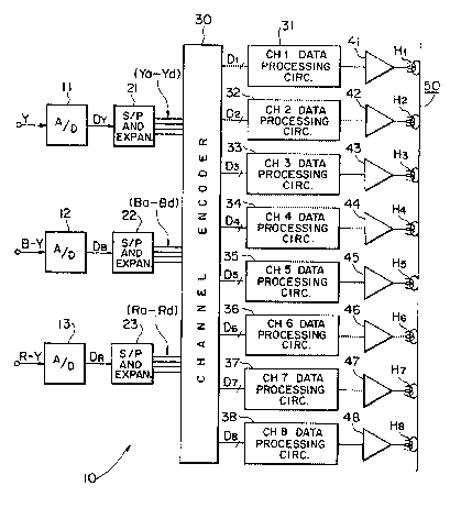
10 includes analog-to-digital (A/D) converters 11, 12 and 13
which individually digitize the input luminance signal Y and
the input first and second component chrominance signals B-Y
and R-Y, respectively, o~ the HDTV video data signals. The
resulting luminance signal data DY and chrominance signal
data DB and DR obtained from the A/D converters 11, 12 and
1~ ,
i ..
i
~3~$~
PATENT
39-0100.2121
13, respecti~ely, are supplied to serial-to-parallel (S/P)-
converters 21, 22 and 23, respectively. ~he S/P convexter
21 converts the luminance signal data DY into four parallel
digital luminance data signals Ya, Yb, Yc and Yd (Fig. 3)
which respectively correspond to four horizontally
contiguous frame segments A, B, C and D shown on Fig. 2 to
be obtained by dividing a frame of the video picture along
vertical lines. Similarly, the S/P converters 22 and 23
convert the digital chrominance data signals DB and DR,
respectively, into four parallel digital chrominance data
signals Ba, Bb; Bc and Bd, and Ra, R~, Rc and Rd,
respectively, which again respectively correspond to the
segments A, B, C and D of a frame of the video picture.
Thç digit~l Yide~-data signals for each frame of
the video picture or imase are comprised of 1920 samples per
horizontal line of the lumlnance signal DY, and 1920 samples
per horizontal line of each of-the chrominance signal data
DB and DR. Accordingly, in the case where the video signals
constituting a horizontal line are divided into four
parallel video data corresponding to the four divided
segments A, B, C and D, the luminance signal data DY fox
each line of a segment are composed of 480 samples and,
similarly, the chrominance signal data DB and DR for each
line of a divided segment are each composed of 480 samples.
Further, in the converters 21, 22 and 23, the four parallel
video data Ya-Yd, Ba-Bd and Ra-Rd, respectively, are
time-expanded, as indicated on Fig. 2, so that the 480
-15~
:~ 3 ~ 2
PATBNT
-39~0100.2121
samples of the luminance signal and of each of the
. chrominance signals making up each horizontal line of each
of the divided segments A, B, C and D will have the same
duration as a horizontal line of a full frame of the video
picture.
The parallel video d~ta from the S/P converters
21, 22 and 23 are supplied to a channel encoder 30 which, as
shown on Pig. 3, includes a delay circuit 301 receiving the
parallel data Ya, Yb, Yc and Yd, and a chroma thinning out
and reorganizing circuit 302 which receives the parallel
data Ba, Bb, Bc and Bd and the parallel data Ra, Rb, Rc and
Rd.
As shown on Figs 7A-7D, the digital chrominance
~data signals Ba-Bd and Ra-Rd applied to the circuit 302 are
thinned-out in the latter, for example, by sub-sampling or
by dropping every other sample of the parallel data,
whereupon the thinned-out or remaining samples of the
chrominance data Ba-.3d and Ra-Rd are respectively mixed with
each other, as shown on Fig. 5, and applied to inputs I5,
I6, I7 and I8 of a so-called barrel shifter 303.
Simultaneously, the parallel luminance data Ya, Yb, Yc and
Yd, after having been delayed for two sampling periods in
the delay circuit 301, are respectively applied to~inputs
Il, I2, I3 and I4 of the barrel shifter 303, as also
indicated on Fig. 5O
-16-
.
PATENT
39-0100~2121
As shown, the barrel shifter 303 has eiyht output
terminals 01, 02, 03,--- 08 which are each selectively
connectable to each of the inputs Il, I2, I3 --- I8, for
example, through-suitable switching circuits (not shown), in
response to 3-bit data applied to a control terminal of the
barrel shifter 303 and representing a control signal S~
which selectively has a counted value from "0" to "7". As
shown on Fig. 4, when the 3-bi~ control data represents the
value "0" of ~he control signal Sc, the output terminals 01,
02, 03, --- 08 of the barrel shifter 303 are connected to
the inputs Il, I2, I3, --- I8, respectively. Similarly,
when the control signal Sc has the value "1", the ou~puts
01, 02, 03, --- 08 of the barrel shifter 303 are connected
to the inpu~s T8,-Ilj-I2, --- I7, respectively.
For providing the 3-bit data constituting the
control signal Sc for the barrel shifter 303, the channel
encoder 30 is further shown on Fig. 3 to include a counter
304 having a reset input R to which a vertical synchronizing
signal separated from ~he video signal being recorded is
applied as a reset pulse. A horizontal line pulse ox
synchronizing signal, also separated from the video signal
being recorded, is supplied to a clock input of the counter
304 so as to be counted up by the latter. The horizontal
synchronizing signal is also supplied, as a load timing
pulse, to a counter 305 which counts up a clock 1/2 C~
having a frequency which is 1/2 that of the sampling pulse
employed in the A/D converters 11, 12 and 13. The count or
-l7-
. ~ 3 11 ~
PATEN~
39-0100.2121
output ~rom the counter 305 is the 3-bit data representiny
the control signal S~. A read only memory (ROM) 306
receives the counted output of the counter 304 and an
odd~even field pulse and, in response to each such
field-pulse the ROM 306 supplies 3-bit initial data
corresponding to the counted value from the counter 304 and
which is applied to a load input L of the counter 305. This
initial 3-bit data applied as load data to the counter 305
determines which data, among the data DATA l-DATA 8 (Fig. 8)
are supplied from ~he channel encoder 30 to each of eight
transmitting channels CH1, CH2, CH3, --- CH8, respectively.
. Since the counter 305 counts the clock l/2 CK
having a frequency which is 1i2 the sampling frequency, it
will be apparent..~hat.the 3-bit.-control data supplied.as
control signal Sc from counter 305 to the barrel shifter 303
changes only every two samples. Accordingly, and as shown
on Fig. 6A, the digital luminance data signals Ya-Yd and the
first and secon~d digital chrominance data signals Ba-Bd and
~a-Rd of the time-expanded picture segments are divided, by
the barrel shifter 303 into respective sets thereof which
each consist of two successive da~a signals. For example,
at the output O1 of the barrel shifter 303, as the control
signal Sc changes its value every two samples, the resulting
output consists of successive sets of digital luminance data
signals, as at Yal, Ya2, and of the first and second digital
chrominancs data signals, as at Bal, Ba3 and Rbl, Rb3.
-18-
. ~
- ' ~ ,
~,
3 ~
PATENT
. 39-0100.2121
As shown on Fig. 3, the outputs 01, 02, 03, --- o~ of the
barrel shifter 303 are connected to a delay circuit 307 in
which the outputs 01, 03, 05, 07 are delayed by two sampling
periods relative to the outputs 02, 04, 06 and 08 for
aligning the heads of the eight parallel streams Dl, D2, D3,
--- D8 of video data on Figs. 1, 3 and 6B.
It will be appreciated from the foregoing that the
channel encoder 30 provides eight parallel streams Dl, D2,
D3, --- D8 of video data DATA 1, DATA 2, DATA 3, --- DATA 8
tFig. 8) of a predetermined data array ~y rearranging the
luminance signal data DY and the chrominance signal data DB
and DR received from the A/D converters 11, 12 and 13,
respectively, by way of the S/P converters 21, 22 and 23,
and then distributes.such eigh~ parallel streams Dl, D2, D3,
--- D8 of video data DATA 1, DATA 2, DATA 3 ---- DATA 8 into
first through eighth channels CHl, CH2, CH3, ---- CH8,
respectively, in a predetermined sequence. As shown on Fig.
1, the eight parallel streams of video data DATA 1, DATA 2,
DATA 3, --- DA~A 8 thus distributed into the channels CH1,
CH2, CH3, --- CH8 are supplied from data processing circuits
31, 32, 33, --- 38, respectively, through recording
amplifiers 41, q2, 43, --- 48, respectively, to eight
magnetic heads H1, H2, H3, --- ~8, respectively, which are
operative to record the received data in 8-channel tracks
which desirably extend obliquely on a magnetic tape 500
--19--
~.
~ 3 ~
PATE~iNT
39-0100.21~1
In the channel encoder 30, the luminance signal
data D~ and the chrominance signal data DB and DR converted
by the S/P converters 21, 22 and 23 into four parallel
streams of data coxresponding to the four divided frame
segments A, B, C and D are further processed so as to
be arranged in sets each comprising two successive samples
o~ the corresponding signal data and arrayed to form the
eight parallel streams of data DATA l, DATA 2, DATA 3, ---
DATA 8, as shown in Fig. 8. It will be seen that, in the
arrangement of Fig. 8, each set Oc two successive samples o
the luminance signal data, for example, as indicated at Yb7,
Yb% in DATA l, is interleaved between sets of two samples o~
the chrominance signal data DB and DR, for example., as
indicated at Ba5,.Ba7 and..at ~b5., Rb7, respectively. In
other words, in each of the eight parallel streams of video
data, each set comprised of two samples of the luminance
signal data DY is interposed between two sets of the
chrominance signal data DB and the chrominance signal data
DR, respectively.
As a result of the described operation of the
channel encoder 30, the four parallel video data Ya-Yd,
Ba-Bd and Ra-Rd provided by the S/P converters 21, 22 and 2~,
in correspondence to the four divided frame segments A, B, C
and D, are rearranged or distributed throughout the eight
parallel streams of data DATA l, DATA 2, DATA 3, --~ DAT~ 8
which are each composed of sets of two successive samples,
as shown on Fig. 8. Furthermore, as shown on Fig. 9, the
-20-
3 ~
PATENT
39-0100.2121
distribution of the eigh~ parallel streams of data to the
individual channels CHl, CH2, CH3, --- CH8 is changed in a
predetermined 8-line se~uence so that the data at the same
horizontal posi~ions on vertically adjacent horizontal lines
of the frame or video picture are distributed to different
channels.
Referring now to Fig. 10, which illustrates the
channels in which the video data representing the divided
frame segment A are distribu~ed, it will be seen that, when
the luminance signal data and the chrominance signal data
converted into four parallel data corresponding to the
divided frame segments A, B, C and D, as described above,
are distributed into the several channels CH1-CH8 by the
channel enc.oder...3Q.in.a manner to ohtain the data
arrangements shown in Figs. 8 and 9, sets of the digital
luminance data signals Ya-Yd, sets of the first digital
chrominance data signals Ba-Bd and sets of the second
digital chrominance data signals Ra-Rd corresponding to
pixels positioned contiguous to each other in adjacent
horizontal lines are respectively distributed into
di ~erent transmission channels. Thus, for example, the
data corresponding to the pixels 9 and 10 in line 5 are
shown on Fig. 10 to be distributed in channel CH2, whereas
the data corresponding to the contiguous pixels 8, 9, 10 and
11 in lines 4 and 6 and the pixels 8 and 11 in line 5 are
distributeA into the other seven channels, that is, into the
', . 1 3 1 l3 ~
.
PATENT
3~-0100~2121
channels CHl, and CH3~CH8. By reason of the foregoing,
errors occurring in transmission in any channel can be
readily corrected and/or concealed on the basis of data
transmitted in the other channels.
Referring now to Fig. 12 which, by way of example,
shows the data processing circuit 31 in the channel C~l, it
will be noted that each of the data processing circuits 31,
32, 33 --- 38 interposed in the channels CH1, CH2, CH3, ---
CH8, respectively, comprises an outer code encoder lO1 which
receives the video data Dl transmitted through the channel
CHl, and which adds thereto, as an error correction code, a
first-direction outer code added to each row of
2-dimensional data formed by 2-dimensionally arraying a
prede.termined.number o'..the...video data in the data stream D1
supplied to the respective first channel CH1. A shuffling
circuit 102 conventionally shuffles the 2-dimensional data
after the addition thereto of the outer code by the encoder
101 and, thereafter, an encoder 103 adds to the
2-dimensional data from the circuit 102, a second-direction
inner code acting as an error corxection code. Further, the
encoder 103 adds a sync word and a block identification code
ID. The next component 104 of the data processing cixcuit
31 is generally operative to effect 8--8 conversion so as to
perform a recording-modulation encoaing operation in respect
to the 2-dimensional data after the addition thereto of the
second-direction inner code, the sync word and the block
identification code ID by the encoder 103. Further, as will
-22-
~ 3 ~
PATENT
3g-0100.2121
be hereinafter described in detail, the clrcuit 104 is
effective ~o invert the data for every other sample, that
is, to invert one of t~e two successive data signals in each
of the sets of digital luminance data signals and in each of
the sets of first and second digital chrominance data
signals so as to achieve a desirable code balance within
each set of two samples or data signal~, even when such code
balance is not adequately achieved by means of 8-8
conversion.
More specifically, and as shown on Fig. 12, the
circuit 104 may desirably include two ROMs 107A and 107B to
which 8-bit video data are selectively input, as address
data, throuyh a switch 106 from the output of the encoder
103. As shown on Figs. 13A and 13B, the ROMs 107A and 107B
have complemsntary tables and, upon being addressed by 8-bit
video data, output 8-8 converted video data. The switch 106
is operated by a swi~ch control signal Sw having a frequency
equal to l/2 the sampling clock fre~uency so that the switch
106 is in the position shown in full lines to supply the
8-bit input, as an address, to the ROM 107A during the first
sample of each set, and to dispose the switch 106 in the
position shown in ~roken lines on Fig. 12 for supplying the
8-bit input as an address to the ROM 107B during the second
sample of the same set. The outputs of the ROMs 107A and
107B are connected together for alternately providing the
output of the circuit 104.
PATENT
39-0100.2121
The operation of the circuit 104 in achieving a
desirable c~de balance within each set of two samples or
data signals, even when such code balance is not adequately
achieved by means of the 8-8 conversion, will now be
described with reierence to Figs. 14A, 14B and 14C. By way
of example, ~ig. 14A shows ~he first three se~s of DATA ;
supplied to the first channel CH1 during the first line of a
frame, and which are shown on Fig. 8 to be comprised of the
set of luminance data signals Ya3, Ya4, the set of
chrominance da.a signals Ba5, Ba7, and the set o. luminance
data signals Yb7, Yb8. ~or the saXe of this explanation,
any influence of the outer and inner codes added in the
encoders 101 and 103 is disregarded.
The luminance data signals Ya3, Ya4, which are
distributed as a set, are assumed to have values represented
by the 8-bit digital sig~als 00100001 and 00100010,
respectively, while the chrominance video signals Ba5, Ba7
which are also distributed as a set, are assumed to have
values corresponding to the 8-bit digital signals 10000000
and 10000001, and the luminance data signals Yb7, Yb8 are
assumed to be represented by the 8-bit digital signals
10101011 and 10100111, respectively, as shown on Fig. 14A.
It is desired that the codes be balanced in each
set of 16-bits of digital data so as to equalize the numbers
of kits that are ~ i and "0". It will be seen that, in the
case of the 16-bit digital data representing the set of
-24-
:
.
- ~ 3 3. ~
PATENT
39-0100.2121
luminance data signals Ya3, Ya4, the ratio of "1" bits to
"0" bits is 4:12, in the case of the 16-bit data
representing ~he chrominance data signals Ba5, Ba7, the
ratio of "1" bits to "0" bits is 3:13, and, in the case of
the 16-bit data representing the luminance data signals Yb7,
Yb8, the ratio of "l" bits to "0" bits is 10:6.
Although the code balance is shown to be improved
in respect to the 16-bit data representing the chrominance
data signals Ba5, Ba7 as a result of the 8-8 convexsion
thereof, that is, the 16-bit data obtained by the 8-8
conversion contains 8 '~l" bits and 8 "0" bits (Fig. 14B?,
corresponding improvement in the code balance is not
obtained in respect to the 16-bits representing the
luminance...data.si.gnals Ya3, Ya4 and the 16-bit data
representing the luminance data signals Yb7, Yb8. Thus, as
shown in Fig. 14B, the 16-bits of data representing the data
signals Ya3, Ya4 contain 4 "1" bits and 12 "0" bits even
after the 8-8 conversion, and the 16-bits of data
representing the luminance data signals Yb7, Yb8 contains 10
"l" bits and 6 "0" bits, a~ter the 8-8 conversion, and these
ratios are not sufficiently balanced.
However, when the 8-bit data representing the
second sample in each o~ the video data sets are inverted to
produce 8-bit data which are complementary to the original
data resulting from the 8-8 conversion, a satisfactory code
balance is obtained in all instances. Thus, in the example
illustrated by Figs. 14A, 14B and 14C, the 8-bit data
-25-
~ 3 1 ~ d
PATENT
39-0100.2121
10100000 which re~ults from the 8-8 conversion of the 8-bit
data representing the luminance data signal Ya4, are
inverted to provide the 8-8 hit data 01011111 shown on Fig.
14C. This results in the 16-bit data representing the video
data set Ya3, Ya4 containing 8 "1" bits and 8 llOII bits.
Similarly, in the case of the video data signals Yb7, Yb8,
the B-bit data 00110111 resulting from the 8-8 conversion of
the data representing the signal Yb8 are inverted to provide
the 8-bit data 11001000 (Fig. 14C). As a result of the
foregoing, the 16-bit data representing the luminance data
signals Yb7, Yb8 after ~he 8-8 conversion and inverting
contains 8 "1" bits and 8 "0" bits. Thus, the sets Ya3, Ya4
and Yb7, Yb8 having inadequate code balances even after the
8-8 conversion are provided with precise code balance by the
inverting of the 8-bit data representing the second video
data signal of each set. Furthermore, where the 8-8
conversion was effective to obtain a proper code balance, as
in the case of the set Ba5, Ba7, the inverting of the 8-bit
data representing the second sample of that set does not
disturb the desirable code balance, as is apparent in Fig.
~4C.
Referring again to Fig. ll, it will be seen that
the data processing circuit 31 is completed by a
parallel-to-series (P/S) converter 105 which receives the
recording-modulation encoded data processed by the
circuit 104 and sequentially converts each transmis.sion
-26-
PATENT
39-0100.2121
block so as to produce serial data at the output of the --
respective channel CHl.
Referring now to Fig. 15, it will be seen that a
reproducing unit 60 of the D-VTR embodying this invention
comprises 8 magne~ic heads Hl, H2, H3, --- H8 adapted to
scan the 8-channel recording tracks on the magnetic tape 50
for reproducing the 8-channel data recorded there~n, and for
supplying the reproduced data through respective reproducin.g
amplifiers 51, 52, S~ 58 to data processing circuits
61, 62, 63, --- 68 which are interposed in ~irst through
eighth channels CHl, CH2, CH3, --- CH8, respectively. The
data processing circuit~ 61, 62, 63, --- 68 are arranged to
process the respective data correspondingly to the
- previously described.data process.ing circuits 31, 32, 33,
--- 38 of the recording unit lO. Thus, the 8-channel video
data Dl, D2, D3, --- D8 are obtained from the reproduced
data by the data processing circuits 61, 62, 63, --- 68 and
supplied to a channel decoder 70. The channel decoder 70
decodes the 8-channel video data Dl, D2, D3 -- D8 in a
manner corresponding to the encoding operation of the
channel encoder 30 in the recording unit, and thereby
provides the luminance data signal DY and ~he chrominance
data signals DB, DR from the video data D1, D2, D3, --- D8.
The luminance data signal DY and the chrominance
signal data signals DB, DR thus obtained from the channel
decoder 70 are processed by error concealing circuits 71, -/2
and 73, respectively, and then are supplied through
.~ -27-
PATENT
39-0100.21~1
parallel-to-serial (P/S) converters 81, 82 and 83,
respectively, to digital-to-analog (D/A) conver~ers 91, 92
and 93. The D/A converters 91, 92 and 93 analoyize the
luminance data signal DY and the chrominance data signals DB
and DR converted previously into serial data by the P/S
converters 81, 82 and 83, and thereby provide the
reproduced luminance signal Y and component chrominance
signals B-~ and R-~ in analog form~
In the reproducing unik 60, the video data Dl, D2,
D3, --- D8 obtained by uniformly dispersing the video data
of the four divided frame segments A, B, C and D throughout
the eight channels CHl, CH2, CH3, --- CH8 are reproduced so
that, even when a fault or increase of the error rate occurs
in one or moxe of the channels, proper error correction
and/or concealment can be carried out effectively in respect
to the reproduced data, and the harmful influence of such
data error on the image quality is dispersed over the entire
picture area or frame for ensuring that deterioration of the
picture quality as a result of such error is not
conspicuous.
Referring now to Fig. 16 which, by way of examp~e,
illustrates the data processing circuit 61 acting on the
reproduced data in the~ first channel C~ll, it will be seen
that each of the data processing circuit 61, 62, 63, --- 68
comprises a serial-to-parallel (S/P) converter 200 for
converting the reproduced data of the respective channel to
-28-
PATENT
39-0100.2121
parallel data. The parallel data from the S/~ convexter 200
is supplied to a circuit 201 which performs-time base
correction thereof and then also performs an 8-8 decoding
conversion which corresponds to the 8-8 encoding conversion
performed in the circuit 109 of the respective data
processing circuit 31 in the recording unit. Thereafter, a
circuit 202 performs error correction using the inner error
correction aode for the reproduced data of the first channel
CHl, whereupon a circuit 203 deshuffles the xeproduced data
in correspondence to the shuffling thereof in the circuit
102 of the data processing circuit 31 of the recording unit.
The resulting video data Dl of the first channel CHl is
finally subjected to error correction in a circuit 204 which
e~ploys the.outer .correction code there~or.
The other data processing circuit 62, 63, --- 68
of the reproducing unit 60 are, as previously noted, similar
to the above descr.ibed.data processing circuit 61 and
similarly act on the reproduced data in the channels CH2,
CH3, --- CH8, respectively, for providing the video data D2,
D3, --- D8 to the channel decoder 70.
It will be seen that, in the transmission of
digital video data signals in accordance with the present
invention, for example, in a D-VTR, a luminance ~ignal and
~irst and second chrominance signals, such as, R-Y and B~Y,
are individually sampled to provide respective digital
luminance data si~nals DY and first and second digital
-29-
PATEN~
39-0100 2121
chrominance data signals DB and DR for forming a
high-definition video picture which is spa~ially divided
into four horizontally contiguous segments A, B, C and D
which are then each time-expanded four times, whereupon the
digital luminance data signals Ya-Yd and the first and
second digital chrominance data signals Ba-Bd and Ra-~d ~re
divided into respective sets thereof which each consist of
two successive data signals, and the sets of digital
luminance and first and second digital chrominance data
signals for each of the segments are distributed into the
transmission channels CHl-CH8 in such a manner that each set
of digital luminance data signals is interleaved between
sets of ~he first and second digital chrominance data
signals.,.respectiuely,. in each..o.the transmission channels,
as clearly shown on Figs. 8 and 9. Further, in accordance
with this invention; one of the two successive data signals,
that is, the second of the data signals forming each of the
sets of dlgital luminance data signals and of first and
second digital chrominance data signals, is inverted, as i.n
the circuit 104 of each of the data processing circuits
31-3~, for obtaining the complement of the one of the t~o
successive data signals in each set which has been inverted,
and thereby substantially minimizing any nc or low-frequency
component in each of the transmission channels.
Although a specific embodiment of the invention
has been described in detail herein with reference to the
-30-
PATENT
39-0100. 2121
accompanying drawings, it is to be understood that the
invention is not limited to that precise embodiment and that
various changes and modification may be effected therein by
one skilled in tha art without departing from the scope or
spirit of the invention as defined in the appended claims.
-31-