Note : Les descriptions sont présentées dans la langue officielle dans laquelle elles ont été soumises.
j 131075~
1 1,7,2,3 ENCODING/DECODING
2EMPLOYING 3/2 FREQUENCY DIVISION
8SPECIFICATION
S This invention relates to data recording and recovery
G systems, and particularly to magnetic data storage and
7 retrieval systems.
9 Run length limited codes have gained significant
recognition in magnetic data storage systems due to their
11 1 ability to increase density of stored data over other forms of
12 ¦ code~ One such code is the (1,7,2,3) code, which has a minimum
13 ¦ of 1 encoded zero between successive encoded ones and a maximum
14 ¦ of 7 encoded zeroes between successive encoded ones, and it has
15 ¦ ~ rate of 2/3, that is, 2 source bits encoded into 3 code
16 I bits~ The advantages of tl,7,~,3) codes are described by T.
17 ¦ Horiguchi and K. Morita, "An Optimization of Modulation codes
18 ¦ in Digital Recording`'r IEEE Transactions on Magnetics, Vol.
9 ~ MAG-12, pp. 740-742, November 1976 G. Jacoby and R. Kost,
¦ "~inary Two-Thirds Rate Code with Full ~ord Look-Ahead", ~EEE
¦ Transactions on Magnetics, Vol. MAG-20, pp. 709~714, September
~2 ¦ 1984 P. H. Siegel, "Recording Codes for Digital Magnetic
~3 ¦ Storage", IEEE Transactions on Magnetics, Vol. MAG-21, pp.
~4 ¦ 1344-1349, September 1985. See also Cohn et al, Patent Number
4,337,458, issued June 29, 1982. One problem associated with
~6 the (1,7,2,3) code is that it requires a voltage controlled
27 oscillator operating at a frequency three times that of the
28 data transfer rate. For data transfer rates of the order of 3fi
29 MHz, the VCO clock is required to operate at 108 MHz.
~1 Stability and reliable self-synchronization of such codes
3~ . ~
~ .
13~U7S6
2 ~ operating at frequencies of the order of 108 ME~Z iS difficult
¦ and costly. For example, Cohn requires clock signals at the
3 ¦ VCO frequency, and at l/2, 1~3, and l/6 that frequency to
4 ¦ operate the code converter. The data transfer rate, which is
5 ¦ l/3 the VCO freguency in the Cohn et al circuit, is limited by
6 ¦ the frequency limitations of the voltage controlled oscillator.
7 l
~ ¦ In principle, LC clock generators can operate at
9 ¦ frequencies in excess of lO0 MHz. However, the values of the
lO ¦ ~C components would be so small as compared to the parasitic
11 ¦ elements that each VCO would require individual tuning and its
l~ ¦ ~requency would vary with small environmental changes. In
13 ¦ addition, such VCOs would exhibit extraordinary problems due to
l~ ¦ radiation, electromagnetic interference and screening
15 ¦ reqirements. Multivibrator~based VCOs, such as used in
16 ¦ computer applications (such as Cohn and the present invention~
17 ¦ are not susceptible to the problems of LC-based VCOs, but
l8 ¦ multivibrator-based VCOs are not capable of operating in excess
19 ¦ o about lO0 MHz using present technologies.
~ I
21 ¦ It is an ob~ect of the present invention to provide an
~2 ¦ ~ncoding system for l,7,2,3 codes wherein the VCO frequency is
~3 ¦ us~d directly as the encoded data clock frequency.
~ I
25 ¦ Another object of the present invention is to provide a
¦ system for derivation of the source data clock and data
2~ ¦ partition clock required for encoding and decoding 1,7,2,3
29 I codes.
31
1 3 1 0756
73834-26
Another object of the present invention is to
provide a 3/2 frequency divider, useful for encoding and
decoding 1,7,2,3 codes.
In accordance with the present invention, ~he VCO
clock signal is operated at a frequency derived from the media
speed (in the case of a write mode) or from the recovered read
pulses (in the case of a read mode). From the VCO frequency,
two additional frequencies are obtained: a frequency of 2/3
V~ ~requency, ~hich is the source data clock frequency, and a
al at 1/3 V~O frequency, which is the data partition clock
~i~nal~ The VCO clock signal, which is also the encoded data
cl~X si~nal, together with the source data clock signal and
~ata partition clock signal, are provided to the encoder~decoder
t~ ~ncode or decode the 1,7,2,3 code.
One feature of the present invention resides in
th~ pro~ision of a novel 3/2 frequency divider which logically
~ivides the pulse frequency from the VCO by 3/2 to derive the
~3 ~ra~uency signal for source data clock.
According to a broad aspect of the invention there
i3 ~rovided apparatus for encoding or decoding data in a
~ ,3 code with a data transfer rate of l/T, where T is the
tim~ int~rval of a source data bit cell, said apparatus com-
~xi3in~ oscillator means responsive to the speed of a recording
m~ n ~hich encoded data is to be recorded to produce a
me~ia speed signal having a frequency f, or responsive to data
to ba decoded recovered from a recording media to produce a
r~ad signal having a frequency f; first divider means responsive
to the signal produced by said oscillator means for producing
a source data clock signal having a frequency e~ual to 2/3 f
and a clock period equal to T; second divider means responsiVe
1 3 1 0756
73834-26
to the signal produced by said oscillator means for producing
a data partition clock signal having a frequency equal to 1~3 f
and a clock period equal to 2T; and converter means responsive
to a source data signal and to said media speed signal and to
said data partition clock signal and to said source data clock
signal to encode said source data in 1,7,2,3 code, or respon~
sive to separated data recovered from said media and to said
read signal and to said data partition clock signal and to
said source data clock signal to decode said separated data
from 1,7,2,3 code.
According to another broad aspect of the invention
there is provided a 3/2 frequency divider responsive to an input
signal having a frequency f to derive an output signal having
a frequency 2/3 f, comprising, in combination: a first D-type
flip-flop having a D input, a clock input, a Q output and a
Q-not output; a second D-type flip-flop having a D input, a
clock input, a Q output and a Q-not output; input means for
providing said input signal to the clock input of said first
D-type flip-flop and for providing an inverse of said input
~0 signal to the clock input of said second D-type flip-flop; first
logic means responsive to the Q-not outputs of said first and
second D-type flip-flops for providing a signal of a first
state to the D inputs of said first and second D-type Elip-
~lops when the Q-not output of either of said D-type flip-
flops is in said first state and for providing a signal of
a second state to the D inputs of said first and second D-type
flip-flops when the Q-not outputs of both of said first and
second D-type flip-flops are in said second state, said first
state being opposite said second state; and second logic means
responsive to the Q outputs of said first and second D-type
- 3a -
1 3 1 0-156
73834-26
flip-flops to provide said output signal.
The above and other features of this invention will
be more fully understood from the following detailed descrip-
tion, and the accompanying drawings, in which:
Figure 1 is a block diagram of a data encoding/
decoding system in accordance with the presently preferred
embodimen~, shown in the data encode or write mode;
- 3b -
1310756
- 4 - 66082-272
Figure 2 is a block diagram of the system shown in
the data decoae read mode;
Figure 3 is a block diagram of a 3/2 frequency di~
vder for use in the circuit illustrated in Figures 1 and 2;
and
Figure 4 is a set of waveforms illustrating operat-
ion of the 3/2 divider illustrated in Figure 3.
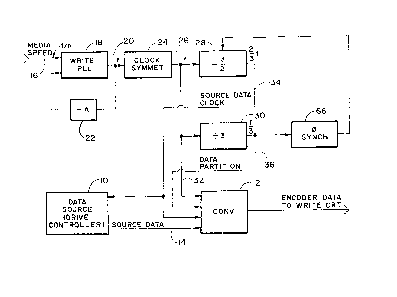
Referring to the drawings, and particularly to Fig-
ure 1, there is illustrated apparatus for encoding 1l7,2,3
code for the write circuits to record onto a magnetic disk
drive. A data source 10, which may conveniently be the disk
drive controller, supplies source data to code converter 12
via channel 14. The source data has a transfer rate equal to
l/T, where T is the time interval of the source data bit cell.
Code converter 12 may be, for example, the encoding circuit
illustrated in Figure 1 of the aforementioned Cohn et al pat-
ent. The source data on channel 14 is described as "data in"
in the aforementioned Cohn et al patent. A signal represent-
ative of the media speed at a frequency of f/n is supplied via
channel 16 to write phase lock loop 18 to provide an output on
channel 20 at a frequency f. The output on channel 20 is pro-
vded through divide by n circuit 22 to the input of write
phase lock loop 18 to lock in the frequency f/n of the signal
on channel 16. Optionally, clock symmetricizer 24 is provided
to provide symmetry to the output signal on channel 26. The
signal on channel 26 is at the desired ~CO frequency f. This
signal is provided as inputs to 3/2 divider 28, divide by 3
circuit 30,
1310756
1 and via channel 32 to converter 12. The signal on channel 32
2 ¦ is provided to input 50 of the converter described in the Cohn
3 ¦ et al patent.
41
5 ¦ Divider 28 provides the source data clock signal on
6 ¦ channel 34 at a frequency of 2~3 f. The source data clock
71 period is equal to T. This signal is provided to ~he data
81 source 10 and to converter 12. Divider 30 provides the data
9¦ partition clock signal at a frequency of 1/3 f to converter
10¦ 12. The data partition clock signal has a period equal to 2T.
11¦ Referring to Fig. 1 of the Cohn et al patent the signal on
~¦ channel 34 is provided to inputs 20 and 23 of Cohn et al, and
13 ¦ the signal on channel 36 is provided to mode control inputs 22
14 ¦ and 48 of Cohn et al.
~51
16 ¦ The operation of converter 12 is, essentially, as
17 ¦ described in the aforementioned Cohn et al patent, except that
18 ¦ the input signals are at the VCO clock frequency f, and at 2/3
19 ¦ and 1/3 f, from dividers 28 and 30. In Cohn et al, on the
20 ¦ other hand, the clock signals are at 1/2, 1/3, and 1/6 the VCO
21 ¦ clock frequency. Thus, the present inven~ion permits operation
22 ¦ o~ the Cohn et al circuit at greater data transfer rates than
heretofore achievable.
~4 I
25 ¦ ~`ig. 2 illustrates the apparatus in the read mode, wherein
2~ ¦ recovered read pulses on channel 38 are applied to read phase
27 ¦ lock loop and VCO 40, which provides the VCO signal on channel
28 ¦ 42 and the separated encoded data on channel 50 to optional
29 ¦ clock symmetricizer 44. A feedback loop 48 from channel 42 is
30 ¦ provided for the phase lock loop and VCO of unit 40. Optional
311
321
1310756
I
1¦ clock symmetricizer 44 provides a signal of frequency f on
21 channel 52 to 3/2 divider 54 lwhich may be identical to the 3/2
31 divider 28 in Fig. 1), to the divide by 3 divider 56 (which may
41 be identical to the divide by 3 divider 30 in Fig 1.) and as a
sl clock input to code converter 46. Converter 46 is the decoder
61 illustrated at Fig. 2 o~ the aforementioned Cohn et al patent,
71 with the separated data on channel 51 from clock ~ rY~
8¦ 44 being the "code in" signal provided to input 60 described in
9¦ the Cohn et al device. The output of 3/2 divider 54 is taken
10¦ via channel 58 to converter 46 and to data receiver 60, which
11¦ m~y conveniently be the drive controller of the magnetic disk
~¦ drive~ Channel 58 carries the source code clock signal at 2/3
~31 the VCO frequency and a time interval equal to T. The output
14 ¦ o~ divider 56 is provided via channel 62 to converter 46.
15¦ Referring to Fig. 2 of Cohn et al, the signal on channel 52 is
16 ¦ provided to inputs 64 and 78 described in Cohn et al, the
17 ¦ signal on channel 58 in provided to input 88 described in
18 ¦ Cohn et al, and the data partition clock signal on channel 62
19 ¦ is provided to input mode control 72, 76, and 86, described in
20 ¦ Cohn et al.
~1 l
¦ Converter 46 operates in the manner as described in the
~3 ¦ Cohn et al patent, except that the input signals are operated
~4 ¦ at the VC0 clock signal frequency, and at signal frequencies
~5 ¦ egual to V3 and 1/3 the VC0 clock signal frequency, rather
~6 ¦ than 1/2, 1~3, and 1/6 of the VCO frequency as described in the
~7 ¦ Cohn et al patent.
28 l
29 ¦ The divide-by-three divider 30 (Fig. 1) and 56 (Fig. 2)
30 ¦ may be simple count-to-three counter. The 3~2 divider 28
31 ¦ (Fig. 1) and 54 (Fig. 2) is shown in greater detail in Fig. 3.
3~ l
1 3 1 0756
l Referring to Fig. 3, there is illustrated a block circuit
~ diagram of a 3/~ frequency divider for use in the
3 encoder/decoder circuit illustrated in Figs. 1 and 2. The
4 circuit illustrated in Fig. 3 is useful in place of blocks 28
and 54 in Figs. 1 and 2. The divider comprises input channel
6 70 for receiving a signal frequency f. ~nit 72 provides
7 separate output complementary signals f and f-not on channels
8 74 and 76 for input to the clock inputs of D-type flip-flops Ql
9 and Q2. The Q~not outputs of flip-flops Ql and Q2 are provided
as separate inputs to OR gate 78 for input to the D inputs of
11 both flip-flops Ql and Q2. The Q outputs of flip-flops Q1 and
12 Q2 are provided as separate inputs to AND gate 80, whose output
13 on channel 82 is the 2/3 frequency signal for input to
14 converters 12 and 46~ data source 10 and data receiver 60 in
Figs. 1 and 2.
16
17 Referring to Fig. 4, the operation of the divider circuit
18 illustrated in Fig. 3 may be explained. Starting at time to
19 the Q outputs of both Ql and Q2 are high and the Q-not outputs
o~ both are low. In this condition, with both Ql and Q2
21 outputs high, the output pulse 90 from AND gate 80 is provided
22 on channel 82, and the output of OR gate 78 is low. At time
23 tl, the f-not signal to the clock input of flip-flop Q2 goes
24 high, thereby resetting flip-flop Q2 so that Q-not output of
1ip-flop Q2 goes high, the Q output of flip-flop Q2 goes low,
26 and the output of OR gate goes high. As a result, the signal
27 on channel 82 goes low. At time t2, the leading edge of
2R pulse signal f is applied to the clock input of flip-flop Ql.
29 However, since the high level from OR gate 78 is applied to the
~ input of flip-flop Ql and the flip-flop is already in a high
31
32
~310756
soate, there is no effect on flip-flop Ql. At time t3, the
leading edge of f-not is applied to the clock input of
3 flip-flop Q2, thereby resetting flip-flop Q2 ~due to the
previously high state of its D input), thereby setting the Q2
output signal high and Q-not output of flip-flop Q2 low. With
6 the Q-not output of Q2 low, the output of OR gate 78 goes low
to the D inputs. With Q output of flip-flop Q2 high, the
8 leading edge of pulse 92 is formed from AND gate 80. At ti~e
t4, the leading edge of pulse f applied to the clock input of
flip-flop Ql. ~ue to the low state of the D input of flip-flop
11 Ql, flip-flop Ql is reset low, thereby terminating pulse 92.
1~¦ The Q-not output of flip-flop Ql is set high, thereby setting
14 ¦ the output of OR gate 78 high to provide high D inputs to both
¦ flip-flops. At time tSr the lead~ng edge of f-not applied to
15 ¦ th~ clock input of flip-flop Q2 has no effect on the flip-flop
16 ¦ Q2 due to the high D input at flip-flop Q2. As a result, the Q
¦ o~tput of flip-flop Q2 remains high and the Q-not output of
18 ¦ flip-flop Q2 remains low. At time t~, the leading edge o~
20 pulse f operates to set flip-flop Ql (due to the previously
~1 hir~h state of the D input) to thereby establish the leading
~2 ed9e of pulse 94~ Also, the Q-not output of flip-flop Ql is
23 terminated, thereby terminating the output from OR gate 78,
~ thereby establishing the conditions at the to line
2~ illustrated in Fig. 4.
~6 Preferrably, phase synchronizer 66 (Fig. 1 & 2) is
28 provided at the outputs of the divide-by-three divider 30
29 (Fig. 1) and 56 (Fig. 2) to provide snort synchronizing pulses
(synch pulses, in Fig. 4) to the overriding set input (S) of
32 j ip-flops Ql and Q2. As shcwn in Fig. 4, the synchronizlng
- 8 -
1 3 1 0 7 5 6
1pulses normally occur (at a frequency of 1/2T or f/3) when both
2 flip-flcps Ql and Q2 are already in their high states.
~ Thereforet the synchronizing pulses do not disturb the
4 synchronous action of the 3~2 divider. The synchronizing
S pulses serve to establish the initial phase relation of the
source data clock signal (from 3/2 divider) with the data
7 partition clock signal from the divide-by-three divider. The
~¦ synchronizing pulses also serve to maintain the correct phase
9¦ relation.
13~
11¦ The present invention thus provides an effective recovery
12 ¦ system for utili2ing 1,7,2,3 code, which does not require the
13 ¦ high fre~uency VCO required by previous systems~ The resu]t,
14 ¦ the system is more effective in operation and makes greater use
15 ¦ of the advantages of the code than over previous systems. The
16 ¦ present invention also provides a novel 2/3 frequency divider.
1~ I
18One feature of the present invention resides in the fact
19 that the data transfer rate is at the clock period T which is
~0 at a }requency of 2/3 f. For a data transfer frequency of 36
21MH~, a VCO ~requency of 54 M~z is required, rather than a 108
2~ MH~ VCO required by Cohn for the same data transfer frequency.
~3 As a result, greater reliability and simplicity of design over
Cohn's approach is achieved.
~5
26This invention is not to be limited by the embodiments
27 shown in the drawings and described in the description, which
28 are given by way of example and not of limitation, but only in
29 accordance with the scope o~ the appended claims.