Note : Les descriptions sont présentées dans la langue officielle dans laquelle elles ont été soumises.
~ 3 ~
~3 62-2G~-L~1
~L~C'l`LIIC DETONATOR OF DELAY TYPE
'l~he present invention generally relates to ,an
electric detonator oE delay type, and rnore paxticularly,
to an electric detonator which i5 preferably used in a
multi-step explosion in which a nurnber of explosives are
05 ignited at diE~erent timings.
l~ kllown electric detonator of delay type com-
prises a pair of leg wires connectable to bus wires
which are connected to an electric blaster, a capacitor
for storing electric energy, an electric delay circuit
including an electronic delay element and an elec~ronic
switchiny element, and an electric igniting portion in-
cluding an igniting resistor and a fuse head applied
thereon. At first, the electric energy is stored in the
capacitor and at a predetermined timing after the elec-
tric blaster has been stopped, the switching element ismade conductive and the electric energy stored in the
capacitor is discharged through the ignitiny resistor to
iynite the detonator.
In the Icnown electric detonator o~ delay type,
it is very important that the amount of electric eneryy
stored in the capacitor, i.e. the terminal voltacJe
across the capacitor, is in a normal operatlon ranye.
That is to say, ~hen the termiIlal voltage across the ca-
- 2- ~
~3~ q 1~3
paci~or is lo~er tllan tIIe lowest vo:ltage of said norlnal
operation range, evell iE the blaster is actuated, a suE-
ficiently large curreIlt does not Elow throucJh the igIlit-
ing resistor and tIIe detorlator is not exploded. To the
05 contrary, when tlle t:ermirIal voltage across the capacitor
exceeds tile hicJIIest: voltaye of the IloLll~al opera~ion
range, the electronic delay circuit micJht not work sat-
isEactorily~ Particlllarly, when the leg wires are erro-
neously connected to the domestic power supply line I
1~) i.e. to E~.C. lO0 V soclcet, the electronic clelay circuit
rmight be brolcen, and in the worst case, the detonator
might be exploded accidentally.
HeretoEore, the safeguard is eEEected oIlly
yiven -the caution or warning that the de-tona-tor should
15 never be connected to supply sources ot~Ier than the
specified one. IIo~7ever, this measure is IlOt suE~icient
for providing the protection against the m; s-operation.
The present invention has for its object to pro-
vide a novel and useEul electric detonator of delay type
20 which can be exploded always under a voltacJe within the
normal operation range and can be exp] oded reliably and
saf ely .
According to the invention, an electric detorIa-
tor oE delay type colnprises
2~ a pair oE leg wires which are connectable to bus
wires connected to a blaster;
- 3 -
a capacitor connected across said ley wires and
storing the electric energy supplied from -the blas-ter
via the bus wires and the leg wires,
a delay circui-t connected to be energi~ed by a ter-
05 minal voltage generated across said capacitor and gener-
ating an igniting signal at a predetermined timing;
a switchiny circuit connected to be made conductive
upon receipt of said igniting signal from said delay
circuit and constituting a discharge passage fo~ the
10 electric energy stored in said capacitor;
an igniting resistor connected in said discharge
passage and igniting the detonator when the electric en-
ergy is discharged through the discharge passage;
a low voltage protection circuit connected across
1~ the leg wires and discharging the electric energy stored
in the capacitor, when a power supply voltage applied
across the leg wires is smaller than the lowest voltage
of a normal operation range; and
a high voltage protection circuit connected across
20 the leg wires and discharging said electric energy
stored in the capacitor when the power supply voltage
exceeds the highest voltage of the normal operation
range and supplying to said delay circuit an inhibit
signal which inhibits a time counting operation of the
2~ delay circuit for determining said predetermined timing.
The invention will now be described with refer-
~ 3 ~ 3
ellce to the a(cc)~ )allyillcJ dr~willcJs, wherei.n:
l~iy. 1 i~ a ~loclc diagram showinc~ all embodimellt
oE the electr.ic detonator of delay type aecording to ~he
invention;
05 Fi~. 2~ is a graph showing the power supply
voltage applied rom the blaster/ and Fiy. 2B is a graph
representing the variation o~ the terminal volkage gen-
erated across tlle eapaeitor; and
Fig. 3 is a circuit diagram illustratiny the de-
tailed eonstruction oE the high and low voltage protec-
tiOII eireuits aceording ko the invention.
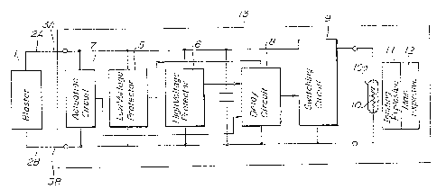
Fig. 1 is a block diagram showing the basie eon-
struetion of the eleetrie detonator of delay type ae-
eording to the invention, the detonator eomprises a pair
1~ o~ leg wires 3A and 3B eonneetable to bus wires 2A and
2s whieh are eonneeted to an electric blaster 1, a ea-
paeitor 4, a low voltage proteetion eireuit 5, high
vol~age proteetion eireuit 6, and an aetuation eireuit
7 r tilese eireuits being conneeted aeross the leg wires
2U 3A and 3s, a delay eireuit 8 triggered by an aetuation
signal supplied Erom the aetuation eireuit 7/ a switeh-
ing eireuit 9 driven by an igniting signal supplied Erom
the delay eircui.t 8, an igniting resistor 10 h~ving a
fuse head lOa applied thereon and eonlleeted to the
s~itehincJ eireuit 9, a igniting explosive .I.l and a rnain
explosive 12. Tile above mell~ioned elelllents are in-
stalled in a housing 13, and the leg wires 3A and 3B areextended out of the housing. The low voltage protection
circuit 5 serves to discharge the electric energy stored
in the capacitor 4, when the power supply voltage ap-
05 plied from the blaster via the bus wires 2A, 2B and legwires 3A, 3B iS lower than the lowest voltage of a nor-
mal operation range. The high voltage protection cir-
cuit 6 serves to discharge the electric energy when the
power supply voltage exceeds the highest voltage of the
normal operation range as well as to supply to the delay
circuit 8 an inhibit signal for inhibiting the time
counting operation in the delay circuit.
Now the operation of -the detonator shown in
Fig. 1 will be explained in detail.
1~ The electric energy supplied from the blaster 1
via the bus wires 2A, 2B and leg wires 3A, 3B is stored
in the capacitor 4. That is to say, as illustrated in
Fig. 2A, the power supply voltage Vo is applied to the
capacitor 4 from the blaster 1 for a period t1-t2.
20 The terminal voltage across the capacitor increases as
shown in Fig. 2B. When the terminal voltage across the
capacitor ~ does not exceed the lowest voltage VL Of the
normal opera-tion range at the timing t2 as illustrated
by a curve I in Fig. 2B, the low voltage protection cir-
2~ cuit 5 is operated to discharge the electric energystored therein. In this case, the delay circuit 8 is
not operated because the electric energy stored in the
capacitor 4 is not supplied to the delay circuit via the
low voltage protection circuit 5. To the contrary, when
the terminal voltage across the capacitor 4 exceeds the
05 highest voltage V~ of the normal operation range during
the time period tl-t2 as shown by a curve lI in Fig. 2B,
the high voltage protection circuit 6 is operated to
discharge the electric energy stored in the capacitor
and to supply the inhibit signal to the delay circui-t 8.
10 Then, in the delay circuit 8, the time counting opera-
tion is forcedly stopped, so that the delay circuit does
not generate the igniting signal. Therefore, in the
above mentioned two cases, the electric detonator is not
exploded.
1~ When the terminal voltage across the capacitor ~
is within the normal operation range as represented by a
curve m in Fig. 2B, both the low voltage protection cir-
cuit 5 and high voltage protecti~n circuit 6 are not op-
erated at all, so that the delay circuit 8 is actuated
20 by the actuating signal which is generated at the timing
t2 by the actuation circuit 7 when the supply voltage is
stopped. The delay circuit 8 operates normally and the
detonator is exploded at a predetermlned timing.
For instance, the delay circuit 8 CompriseS a clock
2~ pulse generator for generating clock pulses having a
constant repetition frequency and a counter which initi-
ales ~O ec-u~ e cl(>clc pu:lses ;n respollse to the actu-
atioll sigl~al al~d geller.~tes tlle ic31litillg signal when the
counter has counte(i the given number of cloek pulses.
The switchirlg circuit 9 is m~de cond~lctive by means oE
0~ the icJniting signal and the electric charye stored in
the capacitor 4 is diseharged through the igniting re-
sistor 10. In the Inanner explailled above, the eleetrie
detoll~tor accordinc3 to the invention is opclated norma:L-
ly only ~7hen tlle power supply voltage is wi~hirl the nor-
10 mal operation range, so that the explosiol~ can be car-
ried out reliabl~ an~ saely.
~ ig. 3 is a circuit diagram illustLating the de-
tailed construction o the detonator shown in Fig. 1.
The low voltaye protection eircuit 5 comprises a
1~ resistor Rl and a capaeitor Cl whose terlninals are
connected to a first main conductor 20A collnected to the
ley wire 3A, a zener diode ZDl connected ~etween a com-
mon junetion point of the other ends oE the resistor Rl
and capacitor Cl and a second main cond~l~tor 20B con-
20 neeted to the leg wire 3B, said ~ener diode having thezener volta~e of, for instanee 27V, a proqran~nable uni-
junction transistor (hereinafter referred to PUT) Pu'rl
having a Eirst base conllect~d to the Eirst main concluc-
tor 20E~, a second base eonnected to the eo~non junction
25 point oE the resistor Rl, capaeitor Cl and zener diode
ZDl, and an emitter coupled with the second main eonduc-
tor 0L3 via a LeSistOr ~2~ NPN type transistor TRl hav-
ing a ~ase conllected to a junction point between the
emitter of PUll and resistor R2 by means o a resistor
R3 all elnitter conl-ected to the second main conductor
05 20s and a col~.ec~or coupled with the first main conduc-
tor 2U~ via a resistor R~ and NPN type trallsistor TR2
having a base connected to the collector oE TRl an
emitter conllected to the second main conc1uctor 2~B and
a collector couple~ with the first mclin con~uctor ~0~ by
10 rneans oE a load resistor RLl~
lhe hiyh volta~e protection eircuit 6 eomprises
a zener diode ZD2 having the zener voltage oE 39 V and
connected between the second main conductor 20B and a
COmlTlOIl jUllCtiOII pOillt oE one ends of resistor R5 and ca-
1~ pacitor c2 whose other ends are connected to the firstmain conduetor 20~ and PUT~ having a first base con-
nected to the ~irst main conductor 20A a second base
connected to the col~lon junction ~oint o~ the resis tor
R5, capacitor C2 and zener diode ZD2 an(l an emi t ter
20 coupled with the second main conductor 2()~ via a load
resistor RL~
The actuation circuit 7 comprises a series cir-
cuit oE diode Dl and resistors ~6 and R7 connected across
the first and second leg wires 3A and 3B and a diode D2
connected between the Eirst leg wire 3~ an~ the irst
main conductor 20A.
,~ .
-
~ hell tlle e:Lectric blaster l is actuated, -the
power suppl~ vo1tage is applied across tlle first and
second main conductors 20A and 20B via the bus wires 2~,
2s and le~ wires 3A, 3B. If this voltaye is lower than
05 a predetermiiled value, i.e. the zener voLtage ~7 V oE
the zener diode ZDl in the low voltage protection cir-
cuit 5, the zener diode ZDL is not made conductiveO
ThereEore, YUT1 remains in the OFF condit:Lon and a base
current oE the trarlsistor TRl does not flow, so that
this transistor 'l`Rl is kept non-conductive. Therefore,
the base current o~ the transistor TR2 flows and this
transistor is made conductive. ~his results in that the
electric energy stored in the capacitor ~1 is discharyed
throucJh the resistor RLl having a low resistan~e and the
15 transistor TR2. In this case, the power supply voltage,
i.e. the electric energy stored in the capacitor 4 is
not supplied Erom an output terminal Pl of the low volt-
age protectioll circuit 5 to the delay circuit 8, so that
the delay circuit does not operate. In -the high voltage
20 protection circuit 6, since the power supply voltage is
lower tharl the zener voltage (39 V) of the zener diode
ZD2, t~-iis zerler diode is not made conductive, and tilUS
PUT2 also remains non-conductive. Therefore, the
high voltage protection circuit 6 does not operate.
2~ When the power supply voltage exceeds the zener
voltage (39 V) oE the zener diode ZD~ of the hiyh volt-
- 10 -
~ 3 ~ 3
~ge protect:ioll circuit 6, tile higll voltage protection
circuit operates as follo~sO Since the zener diode ZD~
is Illade conductiver tl~e base voltage is applied to PU'r2,
50 t~lat PU'1`2 i5 n~de conductive. 'l'herefore, the elec-
o~ tric eneLgy stored in the capacitor 4 is dischargedthrougll the load resistor RL2 having ~ low resistance
and PU'l'2. ~t the sa1lle time, the inhibit signal is sup-
plied Erom the junction point P2 of the resistor RL2 and
PUT2 to the delay circuit 8. Then, the delay circuit ~3
10 stop~ its ti~ne countillg operation. It should be noted
that sil1ce PU'l~ has the self-holdiny property, PUT2
remains conduc-tive until the electric energy in the ca-
pacitor has been ~ully discharged. Further, since the
po~7er supply voltage exceeds the zener voltclc3e ~27 V) o~
15 the zener diode ZDl in the low voltage protection cir-
cuit 5, the ~ener diode zDl, PUTl and TR1 are all made
conductive, and thus TR2 is made non-conductive. There-
Eore, the low voltage protection circuit 5 continues -to
apply the po~er supply voltage ~rom the output terminal
20 Pl to the delay circuit ~.
When the power supply voltage V0 ;~ in the nor-
mal operation range as illustrated by a curve 111 in
Fig. 2B ( 27 V < Vo < 39 V~, the low volt.l~3e protection
eircuit 5 continues to apply the power supply voltage to
Z5 the delay circuit ~ and the high voltage pl-otection cir-
cuit ~ is not actuated and does not produce the inhibi~
signal. Therefore, the actuation signal is generated at
a junction point P3 between the resistors R6 and R7 of
the actuation circuit 7 at the timing t2 at which the
power supply voltage Vo is stopped. Then the delay cir-
0~ cuit 8 initiates to count the clock pulses and generatesthe igniting signal when the predetermined number of
clock pu]ses has been counted. In this manner, the det-
onator is exploded at the predetermined timing.
It should be noted that the low voltage protection cir-
10 cuit 5 continues to operate normally although the termi-
nal voltage across the capacitor is decreased due to the
power consumption at the delay circuit 8, because PUT
has the self holding property.
In the low voltage protection circuit 5, the
15 char~ing time constant of the capacitor ~ is set to be
sufficiently larger than the discharging time constant
o~ the load resistor RLl, and therefore the capacitor 4
can be positively charged.
In the electric detonator of delay type accord-
ing to the invention, the low voltage protection circuit5 can prevent the detonator from being exploded errone-
ously even though the capacitor 4 might be charged with
stray currents such as low voltage noise, and further
the high voltage protection circuit 6 can prevent the
2~ detonator from being exploded acciden-tally even if the
leg wires are erroneously connected to a high volkage
- 1?~-
~ 3 ~ i 3
SUp~)ly ';C)UrCe ~:,UCIl as the (lolllestic L)w~ supply lille,
i.e. i~C lO0 V soclcet a~ld a voltaye supp:Ly source Eor
electric motors. 'i'ilereEore/ the electric detonator ac-
cordill~ to the itlvention is particularly suitable for
05 ci-ty use for clestroyiny large buildings, and fur-ther a
test ~or confir~iny the de-tonator's propert;es can be
effectecl very safely.
~ lhe present invention is not limited -to the em-
bodiln~nt explaine~ above, but may be mocli~ied in various
lU ways. 1~l the a~ove elllbodiment, the low a~ld hiyh voltaye
protection circuits and other circuits are arranyed in
the same housing 13, but these circuits may be installed
in a separate housing and may be connected to the deto-
nator via the leg wires. Further, the low and high
15 voltage protection circuits may be applied to the prilller
o delay type.
In the above embodiment, the normal operation
range is set to 27-39 V, but the lowest voltage VL maY
be set to a value withil~ a range o 3-30 V and the high-
20 est voltage Vll may be selected from a ranye oE 8-54 V in
accordance with the operation voltaye oE the circuitsO
In thls case, it is preferable to determine the normal
operation rancJe by takirlcJ into accoun-t a possible
variation oE the power supply source voltacJe. ~oreover,
2~ in or(ler l~o irlcre~se the sa~eness, the noLIllal operat;io
range has to be set as small as possible.
- 13 -
,, .
As explained above in detail~ accoxding to the
invention, the electric charge stored in the capacitor
is forcedly discharged when the power supply voltage is
out of the normal operation range, so that the electric
05 detonator can be exploded reliably and safely.
Z~
2~
- 14-